From Wikipedia, the free encyclopedia
Potential graphene applications include lightweight, thin, flexible, yet durable display screens, electric circuits, and solar cells, as well as various medical, chemical and industrial processes enhanced or enabled by the use of new graphene materials.
[1]
In 2008,
graphene produced by exfoliation was one of the most expensive materials on Earth, with a sample the area of a cross section of a human hair costing more than $1,000 as of April 2008 (about $100,000,000/cm
2).
[2] Since then, exfoliation procedures have been scaled up, and now companies sell graphene in large quantities.
[3] The price of epitaxial graphene on
Silicon carbide is dominated by the substrate price, which was approximately $100/cm
2 as of 2009.
Hong and his team in South Korea pioneered the synthesis of large-scale graphene films using
chemical vapour deposition (CVD) on thin
nickel layers, which triggered research on practical applications,
[4] with wafer sizes up to 30 inches (760 mm) reported.
[5]
In 2013, the European Union made a €1 billion grant to be used for research into potential graphene applications.
[6]
In 2013 the Graphene Flagship consortium formed, including
Chalmers University of Technology and seven other European universities and research centers, along with
Nokia.
[7]
Medicine
Tissue engineering
Graphene has been investigated for tissue engineering. It has been used as a reinforcing agent to improve the mechanical properties of biodegradable polymeric nanocomposites for engineering bone tissue applications.
[8] Dispersion of low weight % of graphene (~0.02 wt.%) increased in compressive and flexural mechanical properties of polymeric nanocomposites.
Contrast agents/bioimaging
Functionalized and surfactant dispersed graphene solutions have been designed as blood pool
MRI contrast agents.
[9] Additionally,
iodine and
manganese incorporating graphene nanoparticles have served as multimodal MRI-
CT contrast agents.
[10] Graphene micro- and nano-particles have served as contrast agents for
photoacoustic and thermoacoustic tomography.
[11] Graphene has also been reported to be efficiently taken up cancerous cells thereby enabling the design of drug delivery agents for cancer therapy.
[12] Graphene nanoparticles of various morphologies are non-toxic at low concentrations and do not alter stem cell differentiation suggesting that they may be safe to use for biomedical applications.
[13]
Polymerase chain reaction
Graphene is reported to have enhanced
PCR by increasing the yield of
DNA product.
[14] Experiments revealed that graphene's
thermal conductivity could be the main factor behind this result. Graphene yields DNA product equivalent to positive control with up to 65% reduction in PCR cycles.
[citation needed]
Devices
Graphene's modifiable chemistry, large surface area, atomic thickness and molecularly gatable structure make antibody-functionalized graphene sheets excellent candidates for mammalian and microbial detection and diagnosis devices.
[15] Graphene is so thin water has near-perfect
wetting transparency which is an important property particularly in developing bio-sensor applications.
[16] This means that a sensors coated in graphene have as much contact with an aqueous system as an uncoated sensor, while it remains protected mechanically from its environment.
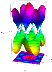
Energy of the electrons with wavenumber
k in graphene, calculated in the
Tight Binding-approximation. The unoccupied (occupied) states, colored in blue–red (yellow–green), touch each other without
energy gap exactly at the above-mentioned six k-vectors.
Integration of graphene (thickness of
6990340000000000000♠0.34 nm) layers as nanoelectrodes into a nanopore
[17] can potentially solve a bottleneck for nanopore-based single-molecule
DNA sequencing.
On November 20, 2013 the
Bill & Melinda Gates Foundation awarded $100,000 'to develop new elastic composite materials for
condoms containing nanomaterials like graphene'.
[18]
In 2014, graphene-based, transparent (across infrared to ultraviolet frequencies), flexible, implantable medical sensor microarrays were announced that allow the viewing of brain tissue hidden by implants. Optical transparency was >90%. Applications demonstrated include optogenetic activation of focal cortical areas,
in vivo imaging of cortical vasculature via fluorescence microscopy and 3D optical coherence tomography.
[19][20]
Drug delivery[edit]
- Researchers in Monash University discovered that the sheet of graphene oxide can be transformed into liquid crystal droplets spontaneously – like a polymer - simply by placing the material in a solution and manipulating the pH. The graphene droplets change their structure at the presence of an external magnetic field. This finding opens the door for potential use of carrying drug in the graphene droplets and drug release upon reaching the targeted tissue when the droplets change shape under the magnetic field. Another possible application is in disease detection if graphene is found to change shape at the presence of certain disease markers such as toxins.[21][22]
- A graphene ‘flying carpet’ was demonstrated to deliver two anti-cancer drugs sequentially to the lung tumor cells (A549 cell) in a mouse model. Doxorubicin (DOX) is embedded onto the graphene sheet, while the molecules of tumor necrosis factor-related apoptosis-inducing ligand (TRAIL) are linked to the nanostructure via short peptide chains. Injected intravenously, the graphene strips with the drug playload preferentially concentrate to the cancer cells due to common blood vessel leakage around the tumor. Receptors on the cancer cell membrane bind TRAIL and cell surface enzymes clip the peptide thus release the drug onto the cell surface. Without the bulky TRAIL, the graphene strips with the embedded DOX are swallowed into the cells. The intracellular acidic environment promotes DOX’s release from graphene. TRAIL on the cell surface triggers the apoptosis while DOX attacks the nucleus. These two drugs work synergistically and were found to be more effective than either drug alone.[23][24]
Biomicrorobotics
Researchers demonstrated a nanoscale biomicrorobot (or cytobot) made by cladding a living endospore cell with graphene quantum dots. The device acted as a humidity sensor.
[25]
Testing
In 2014 a graphene based blood glucose testing product was announced.
[26][27]
Electronics
For
integrated circuits, graphene has a high
carrier mobility, as well as low noise, allowing it to be used as the channel in a
field-effect transistor. Single sheets of graphene are hard to produce and even harder to make on an appropriate substrate.
[28]
In 2008, the smallest transistor so far, one atom thick, 10 atoms wide was made of graphene.
[29] IBM announced in December 2008 that they had fabricated and characterized graphene transistors operating at GHz frequencies.
[30] In May 2009, an n-type transistor was announced meaning that both n and p-type graphene transistors had been created.
[31][32] A functional graphene integrated circuit was demonstrated – a complementary
inverter consisting of one p- and one n-type graphene transistor.
[33] However, this inverter suffered from a very low voltage gain.
According to a January 2010 report,
[34] graphene was epitaxially grown on SiC in a quantity and with quality suitable for mass production of integrated circuits. At high temperatures, the quantum Hall effect could be measured in these samples. IBM built 'processors' using 100 GHz transistors on 2-inch (51 mm) graphene sheets.
[35]
In June 2011, IBM researchers announced that they had succeeded in creating the first graphene-based integrated circuit, a broadband radio mixer.
[36] The circuit handled frequencies up to 10 GHz. Its performance was unaffected by temperatures up to 127 °C.
In June 2013 an 8 transistor 1.28 GHz ring oscillator circuit was described.
[37]
Transistors
Graphene exhibits a pronounced response to perpendicular external electric fields, potentially forming
field-effect transistors (FET). A 2004 paper documented FETs with an on-off ratio of ~30 at room temperature.
[citation needed] A 2006 paper announced an all-graphene planar FET with side gates.
[38] Their devices showed changes of 2% at cryogenic temperatures. The first top-gated FET (on–off ratio of <2 2007.="" class="reference" demonstrated="" id="cite_ref-39" in="" sup="" was="">
[39]
Graphene nanoribbons may prove generally capable of replacing silicon as a semiconductor.
[40]
US patent 7015142 for graphene-based electronics was issued in 2006. In 2008, researchers at
MIT Lincoln Lab produced hundreds of transistors on a single chip
[41] and in 2009, very high frequency transistors were produced at
Hughes Research Laboratories.
[42]
A 2008 paper demonstrated a switching effect based on a reversible chemical modification of the graphene layer that gives an on–off ratio of greater than six orders of magnitude. These reversible switches could potentially be employed in nonvolatile memories.
[43]
In 2009, researchers demonstrated four different types of
logic gates, each composed of a single graphene transistor.
[44]
Practical uses for these circuits are limited by the very small
voltage gain they exhibit. Typically, the amplitude of the output signal is about 40 times less than that of the input signal. Moreover, none of these circuits operated at frequencies higher than 25 kHz.
In the same year, tight-binding numerical simulations
[45] demonstrated that the band-gap induced in graphene bilayer field effect transistors is not sufficiently large for high-performance transistors for digital applications, but can be sufficient for ultra-low voltage applications, when exploiting a tunnel-FET architecture.
[46]
In February 2010, researchers announced transistors with an on/off rate of 100 gigahertz, far exceeding the rates of previous attempts, and exceeding the speed of silicon transistors with an equal gate length. The
6993239990000099999♠240 nm devices were made with conventional silicon-manufacturing equipment.
[47][48][49]
In November 2011, researchers used 3d printing (
additive manufacturing) as a method for fabricating graphene devices.
[50]
In 2013, researchers demonstrated graphene's high mobility in a detector that allows broad band frequency selectivity ranging from the THz to IR region (0.76–33 THz)
[51] A separate group created a terahertz-speed transistor with bistable characteristics, which means that the device can spontaneously switch between two electronic states. The device consists of two layers of graphene separated by an insulating layer of
boron nitride a few atomic layers thick. Electrons move through this barrier by
quantum tunneling. These new transistors exhibit “negative differential conductance,” whereby the same electrical current flows at two different applied voltages.
[52]
Graphene does not have an energy band-gap, which presents a hurdle for its applications in digital logic gates. The efforts to induce a band-gap in graphene via quantum confinement or surface functionalization have not resulted in a breakthrough. The negative differential resistance experimentally observed in graphene field-effect transistors of "conventional" design allows for construction of viable non-Boolean computational architectures with the gap-less graphene. The negative differential resistance — observed under certain biasing schemes — is an intrinsic property of graphene resulting from its symmetric band structure. The results present a conceptual change in graphene research and indicate an alternative route for graphene's applications in information processing.
[53]
In 2013 researchers reported the creation of transistors printed on flexible plastic that operate at 25 gigahertz, sufficient for communications circuits and that can be fabricated at scale. The researchers first fabricate the non-graphene-containing structures—the electrodes and gates—on plastic sheets. Separately, they grow large graphene sheets on metal, then peel it off and transfer it to the plastic. Finally, they top the sheet with a waterproof layer. The devices work after being soaked in water, and are flexible enough to be folded.
[54]
Trilayer graphene
An electric field can change trilayer graphene's crystal structure, transforming its behavior from metal-like to semiconductor-like. A sharp metal
scanning tunneling microscopy tip was able to move the domain border between the upper and lower graphene configurations. One side of the material behaves as a metal, while the other side behaves as a semiconductor. Trilayer graphene can be stacked in either Bernal or
rhombohedral configurations, which can exist in a single flake. The two domains are separated by a precise boundary at which the middle layer is strained to accommodate the transition from one stacking pattern to the other.
[55]
Silicon transistors function as either p-type or
n-type semiconductors, whereas graphene could operate as both. This lowers costs and is more versatile. The technique provides the basis for a
field-effect transistor. Scalable manufacturing techiques have yet to be developed.
[55]
In trilayer graphene, the two stacking configurations exhibit very different electronic properties. The region between them consists of a localized strain
soliton where the carbon atoms of one graphene layer shift by the
carbon–carbon bond distance. The free-energy difference between the two stacking configurations scales quadratically with electric field, favoring rhombohedral stacking as the electric field increases.
[55]
This ability to control the stacking order opens the way to new devices that combine structural and electrical properties.
[55][56]
Graphene-based transistors could be much thinner than modern silicon devices, allowing faster and smaller configurations.
[citation needed]
Transparent conducting electrodes
Graphene's high electrical conductivity and high optical transparency make it a candidate for transparent conducting electrodes, required for such applications as
touchscreens,
liquid crystal displays,
organic photovoltaic cells, and
organic light-emitting diodes. In particular, graphene's mechanical strength and flexibility are advantageous compared to
indium tin oxide, which is brittle. Graphene films may be deposited from solution over large areas.
[57][58]
Large-area, continuous, transparent and highly conducting few-layered graphene films were produced by chemical vapor deposition and used as
anodes for application in
photovoltaic devices. A power conversion efficiency (PCE) up to 1.71% was demonstrated, which is 55.2% of the PCE of a control device based on indium tin oxide.
[59]
Organic light-emitting diodes (OLEDs) with graphene anodes have been demonstrated.
[60] The electronic and optical performance of graphene-based devices are similar to devices made with indium tin oxide.
A carbon-based device called a
light-emitting electrochemical cell (LEC) was demonstrated with chemically-derived graphene as the
cathode and the
conductive polymer PEDOT as the anode.
[61] Unlike its predecessors, this device contains only carbon-based electrodes, with no metal.
[citation needed]
In 2014 a prototype graphene-based flexible display was demonstrated.
[62]
Frequency multiplier
In 2009, researchers built experimental graphene
frequency multipliers that take an incoming signal of a certain frequency and output a signal at a multiple of that frequency.
[63]
Optoelectronics
Graphene strongly interacts with photons, with the potential for direct band-gap creation. This is promising for
optoelectronic and
nanophotonic devices. Light interaction arises due to the
Van Hove singularity. Graphene displays different time scales in response to photon interaction, ranging from femtoseconds (ultra-fast) to picoseconds. Potential uses include transparent films, touch screens and light emitters or as a plasmonic device that confines light and alters wavelengths.
[64]
Hall effect sensors
Due to extremely high electron mobility, graphene may be used for production of highly sensitive
Hall effect sensors.
[65] Potential application of such sensors is connected with DC
current transformers for special applications.
[citation needed]
Quantum dots
Graphene
quantum dots (GQDs) keep all dimensions less than 10 nm. Their size and edge
crystallography govern their electrical, magnetic, optical and chemical properties. GQDs can be produced via graphite nanotomy
[66] or via bottom-up, solution-based routes (
Diels-Alder, cyclotrimerization and/or cyclodehydrogenation reactions).
[67]
GQDs with controlled structure can be incorporated into applications in electronics, optoelectronics and electromagnetics.
Quantum confinement can be created by changing the width of graphene nanoribbons (GNRs) at selected points along the ribbon.
[29][68] It is studied as a catalyst for fuel cells.
[69]
Organic electronics
A semiconducting polymer (
poly(3-hexylthiophene)[70] placed on top of single-layer graphene vertically conducts electric charge better than on a thin layer of silicon. A 50 nm thick polymer film conducted charge about 50 times better than a 10 nm thick film, potentially because the former consists of a mosaic of variably-oriented crystallites forms a continuous pathway of interconnected crystals. In a thin film or on silicon,
[70] plate-like crystallites are oriented parallel to the graphene layer. Uses include solar cells.
[71]
Light processing
Optical modulator
When the
Fermi level of graphene is tuned, its optical absorption can be changed. In 2011, researchers reported the first graphene-based optical modulator. Operating at
7009120000000000000♠1.2 GHz without a temperature controller, this modulator has a broad bandwidth (from 1.3 to 1.6 μm) and small footprint (~
7001250000000000000♠25 μm2).
[72]
Infrared light detection
Graphene, reacts to the infrared spectrum at room temperature, albeit with sensitivity 100 to 1000 times too low for practical applications. However, two graphene layers separated by an insulator allowed an electric field produced by holes left by photo-freed electrons in one layer to affect a current running through the other layer. The process produces little heat, making it suitable for use in night-vision optics. The sandwich is thin enough to be integrated in handheld devices, eyeglass-mounted computers and even
contact lenses.
[73]
Energy
Generation
Ethanol distillation
Graphene oxide membranes allow water vapor to pass through, but are impermeable to other liquids and gases.
[74] This phenomenon has been used for further distilling of
vodka to higher alcohol concentrations, in a room-temperature laboratory, without the application of heat or vacuum as used in traditional
distillation methods.
[75] Further development and commercialization of such membranes could revolutionize the economics of
biofuel production and the
alcoholic beverage industry.
[citation needed]
Solar cells
Graphene has a unique combination of high electrical conductivity and optical transparency, which make it a candidate for use in solar cells. A single sheet of graphene is a zero-bandgap semiconductor whose charge carriers are delocalized over large areas, implying that carrier scattering does not occur. Because this material only absorbs 2.6% of green light and 2.3% of red light,
[76] it is a candidate for applications requiring a transparent conductor.
Graphene can be assembled into a film electrode with low roughness. However, graphene films produced via solution processing contain lattice defects and grain boundaries that act as recombination centers and decrease the material's electrical conductivity. Thus, these films must be made thicker than one atomic layer to obtain useful sheet resistances. This added resistance can be combatted by incorporating conductive filler materials, such as a
silica matrix. Reduced graphene film's electrical conductivity can be improved by attaching large
aromatic molecules such as
pyrene-1-sulfonic acid sodium salt (PyS) and the disodium salt of 3,4,9,10-perylenetetracarboxylic diimide bisbenzenesulfonic acid (PDI). These molecules, under high temperatures, facilitate better π-conjugation of the graphene basal plane. Graphene films have high transparency in the visible and near-
infrared regions and are chemically and thermally stable.
[77]
For graphene to be used in commercial solar cells, large-scale production is required. However, no scalable process for producing graphene is available, including the peeling of pyrolytic graphene or thermal decomposition of silicon carbide.
[77]
Graphene's high charge mobilities recommend it for use as a charge collector and transporter in
photovoltaics (PV). Using graphene as a photoactive material requires its bandgap to be 1.4–1.9 eV. In 2010, single cell efficiencies of nanostructured graphene-based PVs of over 12% were achieved. According to P. Mukhopadhyay and R. K. Gupta
organic photovoltaics could be "devices in which semiconducting graphene is used as the photoactive material and metallic graphene is used as the conductive electrodes".
[77]
In 2010, Xinming Li and Hongwei Zhu from Tsinghua University first reported graphene-silicon heterojunction solar cell, where graphene served as a transparent electrode and introduced a built-in electric field near the interface between the graphene and n-type silicon to help collect photo-generated carriers. More studies promote this new type of photovoltaic device.
[78] For example, in 2012 researchers from the University of Florida reported efficiency of 8.6% for a prototype cell consisting of a wafer of silicon coated with a layer of graphene doped with trifluoromethanesulfonyl-amide (TFSA). Furthermore, Xinming Li found chemical doping could improve the graphene characteristics and significantly enhance the efficiency of graphene-silicon solar cell to 9.6% in 2013.
[79]
In 2015 researchers reported efficiency of 15.6% by choosing the optimal oxide thickness on the silicon.
[80]
In 2013 another team claimed to have reached 15.6% percent using a combination of
titanium oxide and graphene as a charge collector and
perovskite as a sunlight absorber. The device is manufacturable at temperatures under 150 °C (302 °F) using solution-based deposition. This lowers production costs and offers the potential using flexible plastics.
[81]
Large scale production of highly transparent graphene films by
chemical vapor deposition was achieved in 2008. In this process, ultra-thin graphene sheets are created by first depositing carbon atoms in the form of graphene films on a nickel plate from
methane gas. A protective layer of
thermoplastic is laid over the graphene layer and the nickel underneath is dissolved in an acid bath. The final step is to attach the plastic-protected graphene to a flexible
polymer sheet, which can then be incorporated into an OPV cell. Graphene/polymer sheets range in size up to 150 square centimeters and can be used to create dense arrays of flexible OPV cells. It may eventually be possible to run printing presses covering extensive areas with inexpensive solar cells, much like newspaper presses print newspapers (
roll-to-roll).
[82]
Silicon generates only one current-driving electron for each photon it absorbs, while graphene can produce multiple electrons. Solar cells made with graphene could offer 60% conversion efficiency – double the widely accepted maximum efficiency of silicon cells.
[83]
Fuel cells
Appropriately perforated graphene (and hexagonal
boron nitride hBN) can allow
protons to pass through it, offering the potential for using graphene monolayers as a barrier that blocks hydrogen atoms but not protons/ionized hydrogen (hydrogen atoms with their electrons stripped off). They could even be used to extract hydrogen gas out of the atmosphere that could power electric generators with ambient air.
[84]
The membranes are more effective at elevated temperatures and when covered with catalytic nanoparticles such as
platinum.
[84]
Graphene could solve a major problem for fuel cells: fuel crossover that reduces efficiency and durability.
[84]
At room temperature, proton conductivity with monolayer hBN, outperforms graphene, with resistivity to proton flow of about 10 Ω cm
2 and a low activation energy of about 0.3 electronvolts. At higher temperatures, graphene outperforms with resistivity estimated to fall below 10
−3 Ω cm
2 above 250 degrees Celsius.
[85]
In another project, protons easily pass through slightly imperfect graphene membranes on fused
silica in water.
[86] The membrane was exposed to cycles of high and low pH. Protons transferred reversibly from the aqueous phase through the graphene to the other side where they undergo acid–base chemistry with silica hydroxyl groups. Computer simulations indicated energy barriers of 0.61–0.75 eV for hydroxyl-terminated atomic defects that participate in a
Grotthuss-type relay, while
pyrylium-like ether terminations did not.
[87]
Storage
Supercapacitor
Due to graphene's high surface area to mass ratio, one potential application is in the conductive plates of
supercapacitors.
[88]
In February 2013 researchers announced a novel technique to produce graphene
supercapacitors based on the DVD burner reduction approach.
[89]
In 2014 a supercapacitor was announced that was claimed to achieve energy density comparable to current lithium-ion batteries.
[26][27]
In 2015 the technique was adapted to produce stacked, 3-D
supercapacitors. Laser-induced graphene was produced on both sides of a polymer sheet. The sections were then stacked, separated by solid electrolytes, making multiple microsupercapacitors. The stacked configuration substantially increased the energy density of the result. In testing, the researchers charged and discharged the devices for thousands of cycles with almost no loss of capacitance.
[90]
The resulting devices were mechanically flexible, surviving 8,000 bending cycles. This makes them potentially suitable for rolling in a cylindrical configuration. Solid-state polymeric electrolyte-based devices exhibit areal capacitance of >9 mF/cm2 at a current density of 0.02 mA/cm2, over twice that of conventional aqueous electrolytes.
[91]
Also in 2015 another project announced a microsupercapacitor that is small enough to fit in wearable or implantable devices. Just one-fifth the thickness of a sheet of paper, it is capable of holding more than twice as much charge as a comparable thin-film lithium battery. The design employed laser-scribed graphene, or LSG with
manganese dioxide. They can be fabricated without extreme temperatures or expensive “dry rooms”. Their capacity is six times that of commercially available supercapacitors.
[92] The device reached volumetric capacitance of over 1,100 F/cm3. This corresponds to a specific capacitance of the constituent MnO2 of 1,145 F/g, close to the theoretical maximum of 1,380 F/g.
Energy density varies between 22 and 42 Wh/l depending on device configuration.
[93]
Electrode for Li-ion batteries
Stable
Li-ion cycling has recently been demonstrated in bi- and few layer graphene films grown on
nickel substrates,
[94] while single layer graphene films have been demonstrated as a protective layer against corrosion in battery components such as the battery case.
[95] This creates possibilities for flexible electrodes for microscale Li-ion batteries where the anode acts as the active material as well as the current collector.
[96]
There are also
silicon-graphene anode Li-ion batteries.
[97]
Hydrogen storage
Hydrogenation-assisted graphene
origami (HAGO) was used to cause approximately square graphene sheets to fold into a cage can store hydrogen at 9.5 percent by weight. The U.S. Department of Energy had set a goal of 7.5 percent hydrogen by 2020. An electric field causes the box to open and close.
[98]
Rechargeable battery
Researchers at Northwestern University built a
lithium-ion battery made of graphene and
silicon, which was claimed to last over a week on a single charge and only took 15 minutes to charge.
[99]
Sensors
Molecular adsorbtion
Theoretically graphene makes an excellent sensor due to its 2D structure. The fact that its entire volume is exposed to its surrounding environment makes it very efficient to detect
adsorbed molecules. However, similar to carbon nanotubes, graphene has no dangling bonds on its surface. Gaseous molecules cannot be readily adsorbed onto graphene surfaces, so intrinsically graphene is insensitive.
[100] The sensitivity of graphene chemical gas sensors can be dramatically enhanced by functionalization, for example, coating the film with a thin layer of certain polymers. The thin polymer layer acts like a concentrator that absorbs gaseous molecules. The molecule absorption introduces a local change in
electrical resistance of graphene sensors. While this effect occurs in other materials, graphene is superior due to its high electrical conductivity (even when few carriers are present) and low noise, which makes this change in resistance detectable.
[101]
Piezoelectric effect
Density functional theory simulations predict that depositing certain
adatoms on graphene can render it
piezoelectrically responsive to an electric field applied in the out-of-plane direction. This type of locally engineered piezoelectricity is similar in magnitude to that of bulk piezoelectric materials and makes graphene a candidate for control and sensing in nanoscale devices.
[102]
Body motion
Rubber bands infused with graphene("G-bands") can be used as inexpensive body sensors. The bands remain pliable and can be used as a sensor to measure breathing, heart rate, or movement. Lightweight sensor suits for vulnerable patients could make it possible to remotely monitor subtle movement. These sensors display
7001100000000000000♠10-fold increases in resistance and work at strains exceeding 800%. Gauge factors of up to 35 were observed. Such sensors can function at vibration frequencies of at least 160
Hz. At 60 Hz, strains of at least 6% at strain rates exceeding 6000%/s can be monitored.
[103]
Environmental
Contaminant removal
Graphene oxide is non-toxic and biodegradable. Its surface is covered with epoxy, hydroxyl, and carboxyl groups that interact with cations and anions. It is soluble in water and forms stable
colloid suspensions in other liquids because it is
amphiphilic (able to mix with water or oil). Dispersed in liquids it shows excellent
sorption capacities. It can remove copper, cobalt,
cadmium,
arsenate and
organic solvents.
[104]
In 2013 it was shown to be able to remove radioactive
nuclides from water, including radioactive
isotopes of
actinides (elements with atomic numbers 89 to 103, including
thorium,
uranium,
neptunium,
plutonium and
americium) and
lanthanides (the ‘rare earths’ with atomic numbers 57 to 71, including
europium).
[104]
Even at concentrations < 0.1 g/L, radionuclide sorption proceeds rapidly. At pH between 4 and 8, graphene oxide removes over 90% of nuclides, including uranium and europium. At pH >7, more than 70% of strontium and technicium are removed with up to 20% of neptunium.
[104]
Water filtration
Research suggests that graphene filters could outperform other techniques of
desalination by a significant margin.
[105]
Other
Plasmonics and metamaterials
Graphene accommodates a plasmonic surface mode, observed recently via
near field infrared optical microscopy techniques.
[106][107] and infrared spectroscopy
[108] Potential applications are in the terahertz to midinfrared frequencies,
[109] such as terahertz and midinfrared light modulators, passive terahertz filters, midinfrared photodetectors and biosensors.
Lubricant
Scientists discovered using graphene as a
lubricant works better than traditionally used
graphite. A one atom thick layer of graphene in between a steel ball and steel disc lasted for 6,500 cycles. Conventional lubricants lasted 1,000 cycles.
[110]
Radio wave absorption
Stacked graphene layers on a quartz substrate increased the absorption of millimeter (radio) waves by 90 per cent over 125 – 165 GHz bandwidth, extensible to microwave and low-terahertz frequencies, while remaining transparent to visible light. For example, graphene could be used as a coating for buildings or windows to block radio waves. Absorption is a result of mutually coupled
Fabry–Perot resonators represented by each graphene-quartz substrate. A repeated transfer-and-etch process was used to control surface resistivity.
[111][112]
Redox
Graphene oxide can be reversibly reduced and oxidized using electrical stimulus. Controlled reduction and oxidation in two-terminal devices containing multilayer graphene oxide films are shown to result in switching between partially reduced graphene oxide and graphene, a process that modifies electronic and optical properties. Oxidation and reduction are related to resistive switching.
[113]
Nanoantennas
A graphene-based plasmonic nano-antenna (GPN) can operate efficiently at millimeter radio wavelengths. The wavelength of surface
plasmon polaritons for a given frequency is several hundred times smaller than the wavelength of freely propagating electromagnetic waves of the same frequency. These speed and size differences enable efficient graphene-based antennas to be far smaller than conventional alternatives. The latter operate at frequencies 100-1000 times larger than GPNs, producing .01-.001 as many photons.
[114]
An electromagnetic (EM) wave directed vertically onto a graphene surface excites the graphene into oscillations that interact with those in the
dielectric on which the graphene is mounted, thereby forming
surface plasmon polaritons (SPP). When the antenna becomes resonant (an integral number of SPP wavelengths fit into the physical dimensions of the graphene), the SPP/EM coupling increases greatly, efficiently transferring energy between the two.
[114]
A phased array antenna 100
µm in diameter could produce 300 GHz beams only a few degrees in diameter, instead of the 180 degree radiation from tsa conventional metal antenna of that size. Potential uses include
smart dust, low-power terabit
wireless networks[114] and photonics.
[115]
A nanoscale gold rod antenna captured and transformed EM energy into graphene plasmons, analogous to a radio antenna converting radio waves into electromagnetic waves in a metal cable. The plasmon wavefronts can be directly controlled by adjusting antenna geometry. The waves were focused (by curving the antenna) and refracted (by a prism-shaped graphene bilayer because the conductivity in the two-atom-thick prism is larger than in the surrounding one-atom-thick layer.)
[115]
Sound transducers
Graphene provides relatively good
frequency response, suggesting uses in audio speakers. Its light weight may make it suitable for microphones as well.
[116]
Waterproof coating
Graphene could potentially usher in a new generation of waterproof devices whose chassis may not need to be sealed like today's devices.
[99][dubious – discuss]
Coolant additive
Graphene's high thermal conductivity suggests that it could be used as an additive in coolants. Preliminary research work showed that 5% graphene by volume can enhance the thermal conductivity of a base fluid by 86%.
[117]
Another application due to graphene's enhanced thermal conductivity was found in PCR.
[14]
Reference material
Graphene's properties suggest it as a
reference material for characterizing electroconductive and transparent materials. One layer of graphene absorbs 2.3% of red light.
[118]
This property was used to define the
conductivity of transparency that combines
sheet resistance and
transparency.
This parameter was used to compare materials without the use of two independent parameters.
[119]
Thermal management
In 2011, researchers reported that a three-dimensional, vertically aligned, functionalized multilayer graphene architecture can be an approach for graphene-based
thermal interfacial materials (
TIMs) with superior thermal conductivity and ultra-low
interfacial thermal resistance between graphene and metal.
[120]
Graphene-metal composites can be utilized in thermal interface materials.
[121]
Adding a layer of graphene to each side of a copper film increased the metal's heat-conducting properties up to 24%. This suggests the possibility of using them for semiconductor interconnects in computer chips. The improvement is the result of changes in copper’s nano- and microstructure, not from graphene’s independent action as an additional heat conducting channel. High temperature chemical vapor deposition stimulates grain size growth in copper films. The larger grain sizes improve heat conduction. The heat conduction improvement was more pronounced in thinner copper films, which is useful as copper interconnects shrink.
[122]
Structural material
Graphene's strength, stiffness and lightness suggested it for use with
carbon fiber. Graphene has been used as a reinforcing agent to improve the mechanical properties of biodegradable polymeric nanocomposites for engineering bone tissue.
[123]
Catalyst
In 2014, researchers at
The University of Western Australia discovered nano sized fragments of graphene can speed up the rate of
chemical reactions.
[124]


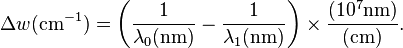
 is the Raman shift expressed in wavenumber, λ0 is the excitation wavelength, and λ1 is the Raman spectrum wavelength. Most commonly, the unit chosen for expressing wavenumber in Raman spectra is inverse centimeters (cm−1). Since wavelength is often expressed in units of nanometers (nm), the formula above can scale for this unit conversion explicitly, giving