Fig. 1. Schematic of plastic solar cells. PET – polyethylene terephthalate, ITO – indium tin oxide, PEDOT:PSS – poly(3,4-ethylenedioxythiophene), active layer (usually a polymer:fullerene blend), Al – aluminium.
An organic solar cell or plastic solar cell is a type of photovoltaic that uses organic electronics, a branch of electronics that deals with conductive organic polymers or small organic molecules,[1] for light absorption and charge transport to produce electricity from sunlight by the photovoltaic effect. Most organic photovoltaic cells are polymer solar cells.
The molecules used in organic solar cells are solution-processable at high throughput and are cheap, resulting in low production costs to fabricate a large volume.[2] Combined with the flexibility of organic molecules, organic solar cells are potentially cost-effective for photovoltaic applications. Molecular engineering (e.g. changing the length and functional group of polymers) can change the band gap, allowing for electronic tunability. The optical absorption coefficient of organic molecules is high, so a large amount of light can be absorbed with a small amount of materials, usually on the order of hundreds of nanometers. The main disadvantages associated with organic photovoltaic cells are low efficiency, low stability and low strength compared to inorganic photovoltaic cells such as silicon solar cells.
Compared to silicon-based devices, polymer solar cells are lightweight (which is important for small autonomous sensors), potentially disposable and inexpensive to fabricate (sometimes using printed electronics), flexible, customizable on the molecular level and potentially have less adverse environmental impact. Polymer solar cells also have the potential to exhibit transparency, suggesting applications in windows, walls, flexible electronics, etc. An example device is shown in Fig. 1. The disadvantages of polymer solar cells are also serious: they offer about 1/3 of the efficiency of hard materials, and experience substantial photochemical degradation.[3]
Polymer solar cells inefficiency and stability problems,[4] combined with their promise of low costs[5] and increased efficiency[6] made them a popular field in solar cell research. As of 2015, polymer solar cells were able to achieve over 10% efficiency via a tandem structure.[7]
Physics

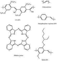
Fig 1: Examples of organic photovoltaic materials
A photovoltaic cell is a specialized semiconductor diode that converts light into direct current (DC) electricity. Depending on the band gap of the light-absorbing material, photovoltaic cells can also convert low-energy, infrared (IR) or high-energy, ultraviolet (UV) photons into DC electricity . A common characteristic of both the small molecules and polymers (Fig 1) used as the light-absorbing material in photovoltaics is that they all have large conjugated systems. A conjugated system is formed where carbon atoms covalently bond with alternating single and double bonds. These hydrocarbons' electrons pz orbitals delocalize and form a delocalized bonding π orbital with a π* antibonding orbital. The delocalized π orbital is the highest occupied molecular orbital (HOMO), and the π* orbital is the lowest unoccupied molecular orbital (LUMO). In organic semiconductor physics, the HOMO takes the role of the valence band while the LUMO serves as the conduction band. The energy separation between the HOMO and LUMO energy levels is considered the band gap of organic electronic materials and is typically in the range of 1–4 eV.[8]
All light with energy greater than the band gap of the material can be absorbed, though there is a trade-off to reducing the band gap as photons absorbed with energies higher than the band gap will thermally give off its excess energy, resulting in lower voltages and power conversion efficiencies. When these materials absorb a photon, an excited state is created and confined to a molecule or a region of a polymer chain. The excited state can be regarded as an exciton, or an electron-hole pair bound together by electrostatic interactions. In photovoltaic cells, excitons are broken up into free electron-hole pairs by effective fields. The effective fields are set up by creating a heterojunction between two dissimilar materials. In organic photovoltaics, effective fields break up excitons by causing the electron to fall from the conduction band of the absorber to the conduction band of the acceptor molecule. It is necessary that the acceptor material has a conduction band edge that is lower than that of the absorber material.[9][10][11][12]
|
||||||||||||||


Polymer solar cells usually consist of an electron- or hole-blocking layer on top of an indium tin oxide (ITO) conductive glass followed by electron donor and an electron acceptor (in the case of bulk heterojunction solar cells), a hole or electron blocking layer, and metal electrode on top. The nature and order of the blocking layers – as well as the nature of the metal electrode – depends on whether the cell follows a regular or an inverted device architecture. In an inverted cell, the electric charges exit the device in the opposite direction as in a normal device because the positive and negative electrodes are reversed. Inverted cells can utilize cathodes out of a more suitable material; inverted OPVs enjoy longer lifetimes than regularly structured OPVs, but they typically don’t reach efficiencies as high as regular OPVs.[13]
In bulk heterojunction polymer solar cells, light generates excitons. Subsequent charge separation in the interface between an electron donor and acceptor blend within the device’s active layer. These charges then transport to the device’s electrodes where the charges flow outside the cell, perform work and then re-enter the device on the opposite side. The cell's efficiency is limited by several factors, especially non-geminate recombination. Hole mobility leads to faster conduction across the active layer.[14][15]
Organic photovoltaics are made of electron donor and electron acceptor materials rather than semiconductor p-n junctions. The molecules forming the electron donor region of organic PV cells, where exciton electron-hole pairs are generated, are generally conjugated polymers possessing delocalized π electrons that result from carbon p orbital hybridization. These π electrons can be excited by light in or near the visible part of the spectrum from the molecule's highest occupied molecular orbital (HOMO) to the lowest unoccupied molecular orbital (LUMO), denoted by a π -π* transition. The energy bandgap between these orbitals determines which wavelength(s) of light can be absorbed.
Unlike in an inorganic crystalline PV cell material, with its band structure and delocalized electrons, excitons in organic photovoltaics are strongly bound with an energy between 0.1 and 1.4 eV. This strong binding occurs because electronic wave functions in organic molecules are more localized, and electrostatic attraction can thus keep the electron and hole together as an exciton. The electron and hole can be dissociated by providing an interface across which the chemical potential of electrons decreases. The material that absorbs the photon is the donor, and the material acquiring the electron is called the acceptor. In Fig. 2, the polymer chain is the donor and the fullerene is the acceptor. Even after dissociation, the electron and hole may still be joined as a "geminate pair", and an electric field is then required to separate them. The electron and hole must be collected at contacts. If charge carrier mobility is insufficient, the carriers will not reach the contacts, and instead recombine at trap sites or remain in the device as undesirable space charges that oppose the flow of new carriers. The latter problem can occur if electron and hole mobilities are not matched. In that case, space-charge limited photocurrent (SCLP) hampers device performance.
Organic photovoltaics can be fabricated with an active polymer and a fullerene-based electron acceptor. Illumination of this system by visible light leads to electron transfer from the polymer to a fullerene molecule. As a result, the formation of a photoinduced quasiparticle, or polaron (P+), occurs on the polymer chain and the fullerene becomes a radical anion (C−
60). Polarons are highly mobile and can diffuse away.
Junction types
The simplest organic PV device features a planar heterojunction (figure 1). A film of organic active material (polymer or small molecule), of electron donor or electron acceptor type is sandwiched between contacts. Excitons created in the active material may diffuse before recombining and separate, hole and electron diffusing to its specific collecting electrode. Because charge carriers have diffusion lengths of just 3–10 nm in typical amorphous organic semiconductors, planar cells must be thin, but the thin cells absorb light less well. Bulk heterojunctions (BHJs) address this shortcoming. In a BHJ, a blend of electron donor and acceptor materials is cast as a mixture, which then phase-separates. Regions of each material in the device are separated by only several nanometers, a distance suited for carrier diffusion. BHJs require sensitive control over materials morphology on the nanoscale. Important variables include materials, solvents and the donor-acceptor weight ratio.The next logical step beyond BHJs are ordered nanomaterials for solar cells, or ordered heterojunctions (OHJs). OHJs minimize the variability associated with BHJs. OHJs are generally hybrids of ordered inorganic materials and organic active regions. For example, a photovoltaic polymer can be deposited into pores in a ceramic such as TiO2. Since holes still must diffuse the length of the pore through the polymer to a contact, OHJs suffer similar thickness limitations. Mitigating the hole mobility bottleneck is key to further enhancing device performance of OHJ's.
Single layer

Fig 2: Sketch of a single layer organic photovoltaic cell
Single layer organic photovoltaic cells are the simplest form. These cells are made by sandwiching a layer of organic electronic materials between two metallic conductors, typically a layer of indium tin oxide (ITO) with high work function and a layer of low work function metal such as Aluminum, Magnesium or Calcium. The basic structure of such a cell is illustrated in Fig 2.
The difference of work function between the two conductors sets up an electric field in the organic layer. When the organic layer absorbs light, electrons will be excited to the LUMO and leave holes in the HOMO, thereby forming excitons. The potential created by the different work functions helps to split the exciton pairs, pulling electrons to the positive electrode (an electrical conductor used to make contact with a non-metallic part of a circuit) and holes to the negative electrode.[9][10][11]
Examples
In 1958 the photovoltaic effect or the creation of voltage of a cell based on magnesium phthalocyanine (MgPc)—a macrocyclic compound having an alternating nitrogen atom-carbon atom ring structure—was discovered to have a photovoltage of 200 mV.[16] An Al/MgPc/Ag cell obtained photovoltaic efficiency of 0.01% under illumination at 690 nm.[17]Conjugated polymers were also used in this type of photovoltaic cell. One device used polyacetylene (Fig 1) as the organic layer, with Al and graphite, producing an open circuit voltage of 0.3 V and a charge collection efficiency of 0.3%.[18] An Al/poly(3-nethyl-thiophene)/Pt cell had an external quantum yield of 0.17%, an open circuit voltage of 0.4 V and a fill factor of 0.3.[19] An ITO/PPV/Al cell showed an open circuit voltage of 1 V and a power conversion efficiency of 0.1% under white-light illumination.[20]
Issues
Single layer organic solar cells do not work well. They have low quantum efficiencies (<1 a="" and="" between="" conductive="" conversion="" difference="" efficiencies="" electric="" electrode.="" electrodes="" electrons="" excitons.="" field="" from="" holes="" is="" low="" major="" often="" p="" power="" problem="" reaching="" recombine="" resulting="" seldom="" split="" sufficient="" that="" the="" them="" to="" two="" with="" without="">Bilayer

Fig 3: Sketch of a multilayer organic photovoltaic cell.
Bilayer cells contain two layers in between the conductive electrodes (Fig 3). The two layers have different electron affinity and ionization energies, therefore electrostatic forces are generated at the interface between the two layers. Light must create excitons in this small charged region for an efficient charge separation and collecting. The materials are chosen to make the differences large enough that these local electric fields are strong, which splits excitons much more efficiently than single layer photovoltaic cells. The layer with higher electron affinity and ionization potential is the electron acceptor, and the other layer is the electron donor. This structure is also called a planar donor-acceptor heterojunction.[9][10][11][12]
Examples
C60 has high electron affinity, making it a good acceptor. A C60/MEH-PPV double layer cell had a relatively high fill factor of 0.48 and a power conversion efficiency of 0.04% under monochromatic illumination.[21] PPV/C60 cells displayed a monochromatic external quantum efficiency of 9%, a power conversion efficiency of 1% and a fill factor of 0.48.[22]Perylene derivatives display high electron affinity and chemical stability. A layer of copper phthalocyanine (CuPc) as electron donor and perylene tetracarboxylic derivative as electron acceptor, fabricating a cell with a fill factor as high as 0.65 and a power conversion efficiency of 1% under simulated AM2 illumination.[23] Halls et al. fabricated a cell with a layer of bis(phenethylimido) perylene over a layer of PPV as the electron donor. This cell had peak external quantum efficiency of 6% and power conversion efficiency of 1% under monochromatic illumination, and a fill factor of up to 0.6.[24]
Issues
The diffusion length of excitons in organic electronic materials is typically on the order of 10 nm. In order for most excitons to diffuse to the interface of layers and split into carriers, the layer thickness should be in the same range as the diffusion length. However, a polymer layer typically needs a thickness of at least 100 nm to absorb enough light. At such a large thickness, only a small fraction of the excitons can reach the heterojunction interface.Discrete heterojunction
A three-layer (two acceptor and one donor) fullerene-free stack achieved a conversion efficiency of 8.4%. The implementation produced high open-circuit voltages and absorption in the visible spectra and high short-circuit currents. Quantum efficiency was above 75% between 400 nm and 720 nm wavelengths, with an open-circuit voltage around 1 V.[25]Bulk heterojunction

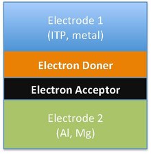
Fig 4: Sketch of a dispersed junction photovoltaic cell
Bulk heterojunctions have an absorption layer consisting of a nanoscale blend of donor and acceptor materials. The domain sizes of this blend are on the order of nanometers, allowing for excitons with short lifetimes to reach an interface and dissociate due to the large donor-acceptor interfacial area.[26] However, efficient bulk heterojunctions need to maintain large enough domain sizes to form a percolating network that allows the donor materials to reach the hole transporting electrode (Electrode 1 in Figure 4) and the acceptor materials to reach the electron transporting electrode (Electrode 2). Without this percolating network, charges might be trapped in a donor or acceptor rich domain and undergo recombination. Bulk heterojunctions have an advantage over layered photoactive structures because they can be made thick enough for effective photon absorption without the difficult processing involved in orienting a layered structure while retaining similar level of performances.
Bulk heterojunctions are most commonly created by forming a solution containing the two components, casting (e.g. drop casting and spin coating) and then allowing the two phases to separate, usually with the assistance of an annealing step. The two components will self-assemble into an interpenetrating network connecting the two electrodes.[27] They are normally composed of a conjugated molecule based donor and fullerene based acceptor. The nanostructural morphology of bulk heterojunctions tends to be difficult to control, but is critical to photovoltaic performance.
After the capture of a photon, electrons move to the acceptor domains, then are carried through the device and collected by one electrode, and holes move in the opposite direction and collected at the other side. If the dispersion of the two materials is too fine, it will result in poor charge transfer through the layer.[10][11][16][28]
Most bulk heterojunction cells use two components, although three-component cells have been explored. The third component, a secondary p-type donor polymer, acts to absorb light in a different region of the solar spectrum. This in theory increases the amount of absorbed light. These ternary cells operate through one of three distinct mechanisms: charge transfer, energy transfer or parallel-linkage.
In charge transfer, both donors contribute directly to the generation of free charge carriers. Holes pass through only one donor domain before collection at the anode. In energy transfer, only one donor contributes to the production of holes. The second donor acts solely to absorb light, transferring extra energy to the first donor material. In parallel linkage, both donors produce excitons independently, which then migrate to their respective donor/acceptor interfaces and dissociate.[29]
Examples
Fullerenes such as C60 and its derivatives are used as electron acceptor materials in bulk heterojunction photovoltaic cells. A cell with the blend of MEH-PPV and a methano-functionalized C60 derivative as the heterojunction, ITO and Ca as the electrodes[30] showed a quantum efficiency of 29% and a power conversion efficiency of 2.9% under monochromatic illumination. Replacing MEH-PPV with P3HT produced a quantum yield of 45% under a 10 V reverse bias.[31][32] Further advances in modifying the electron acceptor has resulted in a device with a power conversion efficiency of 10.61% with a blend of PC71BM as the electron acceptor and PTB7-Th as the electron donor.[33]Polymer/polymer blends are also used in dispersed heterojunction photovoltaic cells. A blend of CN-PPV and MEH-PPV with Al and ITO as the electrodes, yielded peak monochromatic power conversion efficiency of 1% and fill factor of 0.38.[34][35]
Dye sensitized photovoltaic cells can also be considered important examples of this type.
Issues
Fullerenes such as PC71BM are often the electron acceptor materials found in high performing bulk heterojunction solar cells. However, these electron acceptor materials very weakly absorb visible light, decreasing the volume fraction occupied by the strongly absorbing electron donor material. Furthermore, fullerenes have poor electronic tunability, resulting in restrictions placed on the development of conjugated systems with more appealing electronic structures for higher voltages. Recent research has been done on trying to replace these fullerenes with organic molecules that can be electronically tuned and contribute to light absorption.[36]
Graded heterojunction
The electron donor and acceptor are mixed in such a way that the gradient is gradual. This architecture combines the short electron travel distance in the dispersed heterojunction with the advantage of the charge gradient of the bilayer technology.[37][38]Examples
A cell with a blend of CuPc and C60 showed a quantum efficiency of 50% and a power conversion efficiency of 2.1% using 100 mW/cm2 simulated AM1.5G solar illumination for a graded heterojunction.[39]Continuous junction
Similar to the graded heterojunction the continuous junction concept aims at realizing a gradual transition from an electron donor to an electron acceptor. However, the acceptor material is prepared directly from the donor polymer in a post-polymerization modification step.[40]Production
Since its active layer largely determines device efficiency, this component's morphology received much attention.[41]If one material is more soluble in the solvent than the other, it will deposit first on top of the substrate, causing a concentration gradient through the film. This has been demonstrated for poly-3-hexyl thiophene (P3HT), phenyl-C61-butyric acid methyl ester (PCBM) devices where the PCBM tends to accumulate towards the device's bottom upon spin coating from ODCB solutions.[42] This effect is seen because the more soluble component tends to migrate towards the “solvent rich” phase during the coating procedure, accumulating the more soluble component towards the film's bottom, where the solvent remains longer. The thickness of the generated film affects the phases segregation because the dynamics of crystallization and precipitation are different for more concentrated solutions or faster evaporation rates (needed to build thicker devices). Crystalline P3HT enrichment closer to the hole-collecting electrode can only be achieved for relatively thin (100 nm) P3HT/PCBM layers.[43]
The gradients in the initial morphology are then mainly generated by the solvent evaporation rate and the differences in solubility between the donor and acceptor inside the blend. This dependence on solubility has been clearly demonstrated using fullerene derivatives and P3HT.[44] When using solvents which evaporate at a slower rate (as chlorobenzene (CB) or dichlorobenzene (DCB)) you can get larger degrees of vertical separation or aggregation while solvents that evaporate quicker produce a much less effective vertical separation. Larger solubility gradients should lead to more effective vertical separation while smaller gradients should lead to more homogeneous films. These two effects were verified on P3HT:PCBM solar cells.[45][46]
The solvent evaporation speed as well as posterior solvent vapor or thermal annealing procedures were also studied.[47] Blends such as P3HT:PCBM seem to benefit from thermal annealing procedures, while others, such as PTB7:PCBM, seem to show no benefit.[48] In P3HT the benefit seems to come from an increase of crystallinity of the P3HT phase which is generated through an expulsion of PCBM molecules from within these domains. This has been demonstrated through studies of PCBM miscibility in P3HT as well as domain composition changes as a function of annealing times.[49][50][51]
The above hypothesis based on miscibility does not fully explain the efficiency of the devices as solely pure amorphous phases of either donor or acceptor materials never exist within bulk heterojunction devices. A 2010 paper[52] suggested that current models that assume pure phases and discrete interfaces might fail given the absence of pure amorphous regions. Since current models assume phase separation at interfaces without any consideration for phase purity, the models might need to be changed.
The thermal annealing procedure varies depending on precisely when it is applied. Since vertical species migration is partly determined by the surface tension between the active layer and either air or another layer, annealing before or after the deposition of additional layers (most often the metal cathode) affects the result. In the case of P3HT:PCBM solar cells vertical migration is improved when cells are annealed after the deposition of the metal cathode.
Donor or acceptor accumulation next to the adjacent layers might be beneficial as these accumulations can lead to hole or electron blocking effects which might benefit device performance. In 2009 the difference in vertical distribution on P3HT:PCBM solar cells was shown to cause problems with electron mobility which ends up with the yielding of very poor device efficiencies.[53] Simple changes to device architecture – spin coating a thin layer of PCBM on top of the P3HT – greatly enhance cell reproducibility, by providing reproducible vertical separation between device components. Since higher contact between the PCBM and the cathode is required for better efficiencies, this largely increases device reproducibility.
According to neutron scattering analysis, P3HT:PCBM blends have been described as “rivers" (P3HT regions) interrupted by “streams” (PCBM regions).[54]
Solvent effects
Conditions for spin coating and evaporation affect device efficiency.[55][56] Solvent and additives influence donor-acceptor morphology.[57] Additives slow down evaporation, leading to more crystalline polymers and thus improved hole conductivities and efficiencies. Typical additives include 1,8-octanedithiol, ortho-dichlorobenzene, 1,8-diiodooctane (DIO), and nitrobenzene.[45][58][59][60] The DIO effect was attributed to the selective solubilization of PCBM components, modifies fundamentally the average hopping distance of electrons, and thus improves electron mobility.[61] Additives can also lead to big increases in efficiency for polymers.[62] For HXS-1/PCBM solar cells, the effect was correlated with charge generation, transport and shelf-stability.[63] Other polymers such as PTTBO also benefit significantly from DIO, achieving PCE values of more than 5% from around 3.7% without the additive.Polymer Solar Cells fabricated from chloronaphthalene (CN) as a co-solvent enjoy a higher efficiency than those fabricated from the more conventional pure chlorobenzene solution. This is because the donor-acceptor morphology changes, which reduces the phase separation between donor polymer and fullerene. As a result, this translates into high hole mobilities. Without co-solvents, large domains of fullerene form, decreasing photovoltaic performance of the cell due to polymer aggregation in solution. This morphology originates from the liquid-liquid phase separation during drying; solve evaporation causes the mixture to enter into the spinodal region, in which there are significant thermal fluctuations. Large domains prevent electrons from being collected efficiently (decreasing PCE).[64]
Small differences in polymer structure can also lead to significant changes in crystal packing that inevitably affect device morphology. PCPDTBT differs from PSBTBT caused by the difference in bridging atom between the two polymers (C vs. Si), which implies that better morphologies are achievable with PCPDTBT:PCBM solar cells containing additives as opposed to the Si system which achieves good morphologies without help from additional substances.[65]
Self-assembled cells
Supramolecular chemistry was investigated, using donor and acceptor molecules that assemble upon spin casting and heating. Most supramolecular assemblies employ small molecules.[66][67] Donor and acceptor domains in a tubular structure appear ideal for organic solar cells.[68]Diblock polymers containing fullerene yield stable organic solar cells upon thermal annealing.[69] Solar cells with pre-designed morphologies resulted when appropriate supramolecular interactions are introduced.[70]
Progress on BCPs containing polythiophene derivatives yield solar cells that assemble into well defined networks.[71] This system exhibits a PCE of 2.04%. Hydrogen bonding guides the morphology.
Device efficiency based on co-polymer approaches have yet to cross the 2% barrier, whereas bulk-heterojunction devices exhibit efficiencies >7% in single junction configurations.[72]
Fullerene-grafted rod-coil block copolymers have been used to study domain organization.[73]
Supramolecular approaches to organic solar cells provide understanding about the macromolecular forces that drive domain separation.
Infrared polymer cells
Infrared cells preferentially absorb light in the infrared range rather than visible wavelengths. As of 2012, such cells can be made nearly 70% transparent to visible light. The cells allegedly can be made in high volume at low cost using solution processing. Infrared polymer cells can be used as add-on components of portable electronics, smart windows, and building-integrated photovoltaics.The cells employ silver nanowire/titanium dioxide composite films as the top electrode, replacing conventional opaque metal electrodes. With this combination, 4% power-conversion efficiency was achieved.[74]Near-infrared Polymer solar cells based on a copolymer of naphthodithiophene diimide and bithiophene (PNDTI-BT-DT) are also being fabricated in combination with PTB7 as an electron donor. Both PNDTI-BT-DT and PTB7 formed a crystalline structure in the blend films similar to in the pristine films, leading to the efficient charge generation contributed from both polymers.[75]
Power Conversion Efficiency
One of the major issues surrounding polymer solar cells is the low Power Conversion Efficiency (PCE) of fabricated cells. In order to be considered commercial viable, PSCs must be able to achieve at least 10–15% efficiency—this is already much lower than inorganic PVs. However, due to the low cost of polymer solar cells, a 10–15% efficiency is commercially viable.PCE (η) is proportional to the product of the short-circuit current (JSC), the open circuit voltage (VOC), and the fill factor (FF).

Where Pin is the incident solar power. Recent advances in polymer solar cell performance have resulted from compressing the bandgap to enhance short-circuit current while lowering the Highest Occupied Molecular Orbital (HOMO) to increase open-circuit voltage. However, PSCs still suffer from low fill factors (typically below 70%). However, as of 2013, researchers have been able to fabricate PSCs with fill factors of over 75%. Scientists have been able to accomplish via an inverted BHJ and by using nonconventional donor / acceptor combinations.[76]
Commercialization

Number of scientific publications contributing to the subject “polymer solar cell(s)” by year. Search done through ISI, Web of Science.[77]
Polymer solar cells have yet to commercially compete with silicon solar cells and other thin-film cells. The present efficiency of polymer solar cells lies near 10%, well below silicon cells. Polymer solar cells also suffer from environmental degradation, lacking effective protective coatings.
Further improvements in performance are needed to promote charge carrier diffusion; transport must be enhanced through control of order and morphology; and interface engineering must be applied to the problem of charge transfer across interfaces.
Research is being conducted into using tandem architecture in order to increase efficiency of polymer solar cells. Similar to inorganic tandem architecture, organic tandem architecture is expected to increase efficiency. Compared with a single-junction device using low-bandgap materials, the tandem structure can reduce heat loss during photon-to-electron conversion.[7]
Polymer solar cells are not widely produced commercially. Starting in 2008, Konarka Technologies started production of polymer-fullerene solar cells.[78] The initial modules were 3–5% efficient, and only last for a few years. Konarka has since filed for bankruptcy, as those polymer solar cells were unable to penetrate the PV market.
PSCs also still suffer from low fill factors (typically below 70%). However, as of 2013, researchers have been able to fabricate PSCs with fill factors of over 75%. Scientists have been able to accomplish via an inverted BHJ and by using nonconventional donor / acceptor combinations.[76]
However, efforts are being made to upscale manufacturing of polymer solar cells, in order to decrease costs and also advocate for a practical approach for PSC production. Such efforts include full roll-to-roll solution processing. However, roll-to-roll solution processing is ill-suited for on-grid electricity production due to the short lifetime of polymer solar cells. Therefore, commercial applications for polymer solar cells still include primarily consumer electronics and home appliances.[79]
Modeling organic solar cells
As discussed above, organic semiconductors are highly disordered materials with no long range order. This means that the conduction band and valance band edges are not well defined. Furthermore, this physical and energetic disorder generates trap states in which photogenerated electrons and holes can become trapped and then eventually recombine.Key to accurately describing organic solar cells in a device model is to include carrier trapping and recombination via trap states. A commonly used approach is to use an effective medium model, where by standard drift diffusion equations are used to describe transport across the device. Then, an exponential tail of trap states is introduced which decays into the band gap from the mobility edges.[80] To describe capture/escape from these trap states the Shockley–Read–Hall (SRH) can be used. The Shockley-Read-Hall mechanism has been shown able to reproduce polymer:fullerene device behavior in both time domain and steady state.[80]
Current challenges and recent progress
Difficulties associated with organic photovoltaic cells include their low external quantum efficiency (up to 70%)[81] compared to inorganic photovoltaic devices, despite having good internal quantum efficiency; this is due to insufficient absorption with active layers on the order of 100 nanometers. Instabilities against oxidation and reduction, recrystallization and temperature variations can also lead to device degradation and decreased performance over time. This occurs to different extents for devices with different compositions, and is an area into which active research is taking place.[82]Other important factors include the exciton diffusion length, charge separation and charge collection which are affected by the presence of impurities.
Charge carrier mobility and transport
Especially for bulk heterojunction solar cells, understanding charge carrier transport is vital in improving the efficiencies of organic photovoltaics. Currently, bulk heterojunction devices have imbalanced charge-carrier mobility, with the hole mobility being at least an order of magnitude lower than that of the electron mobility; this results in space charge build-up and a decrease in the fill factor and power conversation efficiency of a device.[83] Due to having low mobility, efficient bulk heterojunction photovoltaics have to be designed with thin active layers to avoid recombination of the charge carriers, which is detrimental to absorption and scalability in processing. Simulations have demonstrated that in order to have an bulk heterojunction solar cell with a fill factor above 0.8 and external quantum efficiency above 90%, there needs to be balanced charge carrier mobility to reduce a space charge effect, as well as an increase in charge carrier mobility and/or a decrease in the bimolecular recombination rate constant.[84]Effect of film morphology
-_Highly_folded_Hetero-junction,_(b)-_Hetero-junction_with_controlled_growth.JPG)
Fig 5: Highly folded heterojunction (a); heterojunction with controlled growth (b)
As described above, dispersed heterojunctions of donor-acceptor organic materials have high quantum efficiencies compared to the planar hetero-junction, because in dispersed heterojunctions it is more likely for an exciton to find an interface within its diffusion length. Film morphology can also have a drastic effect on the quantum efficiency of the device. Rough surfaces and the presence of voids can increase the series resistance and also the chance of short-circuiting. Film morphology and, as a result, quantum efficiency can be improved by annealing of a device after covering it by a ~1000 Å thick metal cathode. Metal film on top of the organic film applies stresses on the organic film, which helps to prevent the morphological relaxation in the organic film. This gives more densely packed films and at the same time allows the formation of phase-separated interpenetrating donor-acceptor interface inside the bulk of organic thin film.[85]
Controlled growth heterojunction
Charge separation occurs at the donor-acceptor interface. Whilst traveling to the electrode, a charge can become trapped and/or recombine in a disordered interpenetrating organic material, resulting in decreased device efficiency. Controlled growth of the heterojunction provides better control over positions of the donor-acceptor materials, resulting in much greater power efficiency (ratio of output power to input power) than that of planar and highly disoriented hetero-junctions (as shown in Fig 5). Thus, the choice of suitable processing parameters in order to better control the structure and film morphology is highly desirable.[29]Progress in growth techniques
Mostly organic films for photovoltaic applications are deposited by spin coating and vapor-phase deposition. However each method has certain draw backs, spin coating technique can coat larger surface areas with high speed but the use of solvent for one layer can degrade the already existing polymer layer. Another problem is related with the patterning of the substrate for device as spin-coating results in coating the entire substrate with a single material.Vacuum thermal evaporation
_Vapor_thermal_Evaporation.JPG)
Fig 6: Vacuum thermal evaporation (a) and organic phase vapor deposition (b)
Another deposition technique is vacuum thermal evaporation (VTE) which involves the heating of an organic material in vacuum. The substrate is placed several centimeters away from the source so that evaporated material may be directly deposited onto the substrate, as shown in Fig 6(a). This method is useful for depositing many layers of different materials without chemical interaction between different layers. However, there are sometimes problems with film-thickness uniformity and uniform doping over large-area substrates. In addition, the materials that deposit on the wall of the chamber can contaminate later depositions. This "line of sight" technique also can create holes in the film due to shadowing, which causes an increase in the device series-resistance and short circuit.[86]
Organic vapor phase deposition
Organic vapor phase deposition (OVPD, Fig 6(b)) allows better control of the structure and morphology of the film than vacuum thermal evaporation. The process involves evaporation of the organic material over a substrate in the presence of an inert carrier gas. The resulting film morphology can be tuned by changing the gas flow rate and the source temperature. Uniform films can be grown by reducing the carrier gas pressure, which will increase the velocity and mean free path of the gas, and as a result boundary layer thickness decreases. Cells produced by OVPD do not have issues related with contaminations from the flakes coming out of the walls of the chamber, as the walls are warm and do not allow molecules to stick to and produce a film upon them.Another advantage over VTE is the uniformity in evaporation rate. This occurs because the carrier gas becomes saturated with the vapors of the organic material coming out of the source and then moves towards the cooled substrate, Fig. 6(b). Depending on the growth parameters (temperature of the source, base pressure and flux of the carrier gas) the deposited film can be crystalline or amorphous in nature. Devices fabricated using OVPD show a higher short-circuit current density than that of devices made using VTE. An extra layer of donor-acceptor hetero-junction at the top of the cell may block excitons, whilst allowing conduction of electron; resulting in improved cell efficiency.[86]