Search This Blog

Sunday, July 1, 2018

Nanomaterials

From Wikipedia, the free encyclopedia

Nanomaterials describe, in principle, materials of which a single unit is sized (in at least one dimension) between 1 to 1000 nanometres (10−9 meter) but usually is 1 to 100 nm (the usual definition of nanoscale[1]).

Nanomaterials research takes a materials science-based approach to nanotechnology, leveraging advances in materials metrology and synthesis which have been developed in support of microfabrication research. Materials with structure at the nanoscale often have unique optical, electronic, or mechanical properties.[2]

Nanomaterials are slowly becoming commercialized[3] and beginning to emerge as commodities.[4]

Definition

There are significant differences among agencies on the definition of a nanomaterial.[5]

In ISO/TS 80004, nanomaterial is defined as a "material with any external dimension in the nanoscale or having internal structure or surface structure in the nanoscale", with nanoscale defined as the "length range approximately from 1 nm to 100 nm". This includes both nano-objects, which are discrete pieces of material, and nanostructured materials, which have internal or surface structure on the nanoscale; a nanomaterial may be a member of both these categories.[6]

On 18 October 2011, the European Commission adopted the following definition of a nanomaterial: "A natural, incidental or manufactured material containing particles, in an unbound state or as an aggregate or as an agglomerate and for 50% or more of the particles in the number size distribution, one or more external dimensions is in the size range 1 nm – 100 nm. In specific cases and where warranted by concerns for the environment, health, safety or competitiveness the number size distribution threshold of 50% may be replaced by a threshold between 1% to 50%."[7]

Sources

Engineered

Engineered nanomaterials have been deliberately engineered and manufactured by humans to have certain required properties.[8]

Legacy nanomaterials are those that were in commercial production prior to the development of nanotechnology as incremental advancements over other colloidal or particulate materials.[9][10][11] They include carbon black and titanium dioxide nanoparticles.[12]

Incidental

Nanomaterials may be incidentally produced as a byproduct of mechanical or industrial processes.Sources of incidental nanoparticles include vehicle engine exhausts, welding fumes, combustion processes from domestic solid fuel heating and cooking. Incidental atmospheric nanoparticles are often referred to as ultrafine particles, and are a contributor to air pollution.[13]

Natural

Biological systems often feature natural, functional nanomaterials. The structure of foraminifera (mainly chalk) and viruses (protein, capsid), the wax crystals covering a lotus or nasturtium leaf, spider and spider-mite silk,[14] the blue hue of tarantulas,[15] the "spatulae" on the bottom of gecko feet, some butterfly wing scales, natural colloids (milk, blood), horny materials (skin, claws, beaks, feathers, horns, hair), paper, cotton, nacre, corals, and even our own bone matrix are all natural organic nanomaterials.

Natural inorganic nanomaterials occur through crystal growth in the diverse chemical conditions of the Earth's crust. For example, clays display complex nanostructures due to anisotropy of their underlying crystal structure, and volcanic activity can give rise to opals, which are an instance of a naturally occurring photonic crystals due to their nanoscale structure. Fires represent particularly complex reactions and can produce pigments, cement, fumed silica etc.

Natural sources of nanoparticles include combustion products forest fires, volcanic ash, ocean spray, and the radioactive decay of radon gas. Natural nanomaterials can also be formed through weathering processes of metal- or anion-containing rocks, as well as at acid mine drainage sites.[13]
Gallery of natural nanomaterials

Types

Nano-objects are often categorized as to how many of their dimensions fall in the nanoscale. A nanoparticle is defined a nano-object with all three external dimensions in the nanoscale, whose longest and the shortest axes do not differ significantly. A nanofiber has two external dimensions in the nanoscale, with nanotubes being hollow nanofibers and nanorods being solid nanofibers. A nanoplate has one external dimension in the nanoscale, and if the two larger dimensions are significantly different it is called a nanoribbon. For nanofibers and nanoplates, the other dimensions may or may not be in the nanoscale, but must be significantly larger. A significant different in all cases is noted to be typically at least a factor of 3.[16]

Nanostructured materials are often categorized by what phases of matter the contain. A nanocomposite is a solid containing at least one physically or chemically distinct region, or collection of regions, having at least one dimension in the nanoscale.. A nanofoam has a liquid or solid matrix, filled with a gaseous phase, where either phase has dimensions on the nanoscale. A nanoporous material is a solid material containing nanopores, cavities with dimensions on the nanoscale. A nanocrystalline material has a significant fraction of crystal grains in the nanoscale.[17]

The above definitions are all according to ISO/TS 80004. In other sources, nanoporous materials and nanofoam are sometimes considered nanostructures but not nanomaterials because only the voids and not the materials themselves are nanoscale.[18] Although the ISO definition only considers round nano-objects to be nanoparticles, other sources use the term nanoparticle for all shapes.[19]

Nanoparticles

Nanoparticles have all three dimensions on the nanoscale. Nanoparticles can also be embedded in a bulk solid to form a nanocomposite.[18]

Fullerenes

The fullerenes are a class of allotropes of carbon which conceptually are graphene sheets rolled into tubes or spheres. These include the carbon nanotubes (or silicon nanotubes) which are of interest both because of their mechanical strength and also because of their electrical properties.[20]

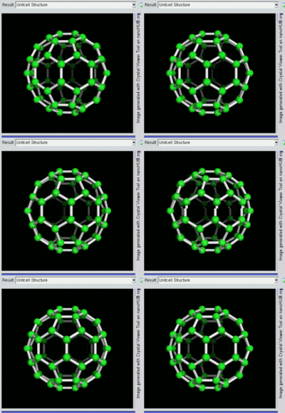
Rotating view of C60, one kind of fullerene.

The first fullerene molecule to be discovered, and the family's namesake, buckminsterfullerene (C60), was prepared in 1985 by Richard Smalley, Robert Curl, James Heath, Sean O'Brien, and Harold Kroto at Rice University. The name was a homage to Buckminster Fuller, whose geodesic domes it resembles. Fullerenes have since been found to occur in nature.[21] More recently, fullerenes have been detected in outer space.[22]

For the past decade, the chemical and physical properties of fullerenes have been a hot topic in the field of research and development, and are likely to continue to be for a long time. In April 2003, fullerenes were under study for potential medicinal use: binding specific antibiotics to the structure of resistant bacteria and even target certain types of cancer cells such as melanoma. The October 2005 issue of Chemistry and Biology contains an article describing the use of fullerenes as light-activated antimicrobial agents. In the field of nanotechnology, heat resistance and superconductivity are among the properties attracting intense research.

A common method used to produce fullerenes is to send a large current between two nearby graphite electrodes in an inert atmosphere. The resulting carbon plasma arc between the electrodes cools into sooty residue from which many fullerenes can be isolated.

There are many calculations that have been done using ab-initio Quantum Methods applied to fullerenes. By DFT and TDDFT methods one can obtain IR, Raman and UV spectra. Results of such calculations can be compared with experimental results.

Metal-based nanoparticles

Inorganic nanomaterials, (e.g. quantum dots, nanowires and nanorods) because of their interesting optical and electrical properties, could be used in optoelectronics.[23] Furthermore, the optical and electronic properties of nanomaterials which depend on their size and shape can be tuned via synthetic techniques. There are the possibilities to use those materials in organic material based optoelectronic devices such as Organic solar cells, OLEDs etc. The operating principles of such devices are governed by photoinduced processes like electron transfer and energy transfer. The performance of the devices depends on the efficiency of the photoinduced process responsible for their functioning. Therefore, better understanding of those photoinduced processes in organic/inorganic nanomaterial composite systems is necessary in order to use them in optoelectronic devices.

Nanoparticles or nanocrystals made of metals, semiconductors, or oxides are of particular interest for their mechanical, electrical, magnetic, optical, chemical and other properties.[24][25] Nanoparticles have been used as quantum dots and as chemical catalysts such as nanomaterial-based catalysts. Recently, a range of nanoparticles are extensively investigated for biomedical applications including tissue engineering, drug delivery, biosensor.[26] [27]

Nanoparticles are of great scientific interest as they are effectively a bridge between bulk materials and atomic or molecular structures. A bulk material should have constant physical properties regardless of its size, but at the nano-scale this is often not the case. Size-dependent properties are observed such as quantum confinement in semiconductor particles, surface plasmon resonance in some metal particles and superparamagnetism in magnetic materials.

Nanoparticles exhibit a number of special properties relative to bulk material. For example, the bending of bulk copper (wire, ribbon, etc.) occurs with movement of copper atoms/clusters at about the 50 nm scale. Copper nanoparticles smaller than 50 nm are considered super hard materials that do not exhibit the same malleability and ductility as bulk copper. The change in properties is not always desirable. Ferroelectric materials smaller than 10 nm can switch their magnetisation direction using room temperature thermal energy, thus making them useless for memory storage. Suspensions of nanoparticles are possible because the interaction of the particle surface with the solvent is strong enough to overcome differences in density, which usually result in a material either sinking or floating in a liquid. Nanoparticles often have unexpected visual properties because they are small enough to confine their electrons and produce quantum effects. For example, gold nanoparticles appear deep red to black in solution.

The often very high surface area to volume ratio of nanoparticles provides a tremendous driving force for diffusion, especially at elevated temperatures. Sintering is possible at lower temperatures and over shorter durations than for larger particles. This theoretically does not affect the density of the final product, though flow difficulties and the tendency of nanoparticles to agglomerate do complicate matters. The surface effects of nanoparticles also reduces the incipient melting temperature.

One-dimensional nanostructures

The smallest possible crystalline wires with cross-section as small as a single atom can be engineered in cylindrical confinement [28][29][30]. Carbon nanotubes, a natural semi-1D nanostructure, can be used as a template for synthesis. Confinement provides mechanical stabilization and prevents linear atomic chains from disintegration; other structures of 1D nanowires are predicted to be mechanically stable even upon isolation from the templates [31][32].

Two-dimensional nanostructures

2D materials are crystalline materials consisting of a two-dimensional single layer of atoms. The most important representative graphene was discovered in 2004.

Box-shaped graphene (BSG) nanostructure is an example of 3D nanomaterial.[33] BSG nanostructure has appeared after mechanical cleavage of pyrolytic graphite. This nanostructure is a multilayer system of parallel hollow nanochannels located along the surface and having quadrangular cross-section. The thickness of the channel walls is approximately equal to 1 nm. The typical width of channel facets makes about 25 nm.

Thin films with nanoscale thicknesses are considered nanostructures, but are sometimes not considered nanomaterials because they do not exist separately from the substrate.[18]

Bulk nanostructured materials

Some bulk materials contain features on the nanoscale, including nanocomposites, nanocrystalline materials, nanostructured films, and nanotextured surfaces.[18]

Applications

Nano materials are used in a variety of, manufacturing processes, products and healthcare including paints, filters, insulation and lubricant additives. In healthcare Nanozymes are nanomaterials with enzyme-like characteristics.[34] They are an emerging type of artificial enzyme, which have been used for wide applications in such as biosensing, bioimaging, tumor diagnosis,[35] antibiofouling and more. In paints nanomaterials are used to improve UV protection and improve ease of cleaning.[36] High quality filters may be produced using nanostructures, these filters are capable of removing particulate as small as a virus as seen in a water filter created by Seldon Technologies. In the air purification field, nano technology was used to combat the spread of MERS in Saudi Arabian hospitals in 2012.[37] Nanomaterials are being used in modern and human-safe insulation technologies, in the past they were found in Asbestos-based insulation.[38] As a lubricant additive, nano materials have the ability to reduce friction in moving parts. Worn and corroded parts can also be repaired with self-assembling anisotropic nanoparticles called TriboTEX.[37]

Synthesis

The goal of any synthetic method for nanomaterials is to yield a material that exhibits properties that are a result of their characteristic length scale being in the nanometer range (1 – 100 nm).

Accordingly, the synthetic method should exhibit control of size in this range so that one property or another can be attained. Often the methods are divided into two main types "Bottom Up" and "Top Down."

Bottom up methods

Bottom up methods involve the assembly of atoms or molecules into nanostructured arrays. In these methods the raw material sources can be in the form of gases, liquids or solids. The latter requiring some sort of disassembly prior to their incorporation onto a nanostructure. Bottom methods generally fall into two categories: chaotic and controlled.

Chaotic processes involve elevating the constituent atoms or molecules to a chaotic state and then suddenly changing the conditions so as to make that state unstable. Through the clever manipulation of any number of parameters, products form largely as a result of the insuring kinetics. The collapse from the chaotic state can be difficult or impossible to control and so ensemble statistics often govern the resulting size distribution and average size. Accordingly, nanoparticle formation is controlled through manipulation of the end state of the products. Examples of Chaotic Processes are: Laser ablation, Exploding wire, Arc, Flame pyrolysis, Combustion, Precipitation synthesis techniques.

Controlled Processes involve the controlled delivery of the constituent atoms or molecules to the site(s) of nanoparticle formation such that the nanoparticle can grow to a prescribed sizes in a controlled manner. Generally the state of the constituent atoms or molecules are never far from that needed for nanoparticle formation. Accordingly, nanoparticle formation is controlled through the control of the state of the reactants. Examples of controlled processes are self-limiting growth solution, self-limited chemical vapor deposition, shaped pulse femtosecond laser techniques, and molecular beam epitaxy.

Characterization

Novel effects can occur in materials when structures are formed with sizes comparable to any one of many possible length scales, such as the de Broglie wavelength of electrons, or the optical wavelengths of high energy photons. In these cases quantum mechanical effects can dominate material properties. One example is quantum confinement where the electronic properties of solids are altered with great reductions in particle size. The optical properties of nanoparticles, e.g. fluorescence, also become a function of the particle diameter. This effect does not come into play by going from macrosocopic to micrometer dimensions, but becomes pronounced when the nanometer scale is reached.
In addition to optical and electronic properties, the novel mechanical properties of many nanomaterials is the subject of nanomechanics research. When added to a bulk material, nanoparticles can strongly influence the mechanical properties of the material, such as the stiffness or elasticity. For example, traditional polymers can be reinforced by nanoparticles (such as carbon nanotubes) resulting in novel materials which can be used as lightweight replacements for metals. Such composite materials may enable a weight reduction accompanied by an increase in stability and improved functionality.[39]

Finally, nanostructured materials with small particle size such as zeolites, and asbestos, are used as catalysts in a wide range of critical industrial chemical reactions. The further development of such catalysts can form the basis of more efficient, environmentally friendly chemical processes.

The first observations and size measurements of nano-particles were made during the first decade of the 20th century. Zsigmondy made detailed studies of gold sols and other nanomaterials with sizes down to 10 nm and less. He published a book in 1914.[40] He used an ultramicroscope that employs a dark field method for seeing particles with sizes much less than light wavelength.

There are traditional techniques developed during 20th century in Interface and Colloid Science for characterizing nanomaterials. These are widely used for first generation passive nanomaterials specified in the next section.

These methods include several different techniques for characterizing particle size distribution. This characterization is imperative because many materials that are expected to be nano-sized are actually aggregated in solutions. Some of methods are based on light scattering. Others apply ultrasound, such as ultrasound attenuation spectroscopy for testing concentrated nano-dispersions and microemulsions.[41]

There is also a group of traditional techniques for characterizing surface charge or zeta potential of nano-particles in solutions. This information is required for proper system stabilzation, preventing its aggregation or flocculation. These methods include microelectrophoresis, electrophoretic light scattering and electroacoustics. The last one, for instance colloid vibration current method is suitable for characterizing concentrated systems.

Uniformity

The chemical processing and synthesis of high performance technological components for the private, industrial and military sectors requires the use of high purity ceramics, polymers, glass-ceramics and material composites. In condensed bodies formed from fine powders, the irregular sizes and shapes of nanoparticles in a typical powder often lead to non-uniform packing morphologies that result in packing density variations in the powder compact.

Uncontrolled agglomeration of powders due to attractive van der Waals forces can also give rise to in microstructural inhomogeneities. Differential stresses that develop as a result of non-uniform drying shrinkage are directly related to the rate at which the solvent can be removed, and thus highly dependent upon the distribution of porosity. Such stresses have been associated with a plastic-to-brittle transition in consolidated bodies, and can yield to crack propagation in the unfired body if not relieved.[42][43] [44]

In addition, any fluctuations in packing density in the compact as it is prepared for the kiln are often amplified during the sintering process, yielding inhomogeneous densification. Some pores and other structural defects associated with density variations have been shown to play a detrimental role in the sintering process by growing and thus limiting end-point densities. Differential stresses arising from inhomogeneous densification have also been shown to result in the propagation of internal cracks, thus becoming the strength-controlling flaws. [45][46]

It would therefore appear desirable to process a material in such a way that it is physically uniform with regard to the distribution of components and porosity, rather than using particle size distributions which will maximize the green density. The containment of a uniformly dispersed assembly of strongly interacting particles in suspension requires total control over particle-particle interactions. It should be noted here that a number of dispersants such as ammonium citrate (aqueous) and imidazoline or oleyl alcohol (nonaqueous) are promising solutions as possible additives for enhanced dispersion and deagglomeration. Monodisperse nanoparticles and colloids provide this potential.[47]

Monodisperse powders of colloidal silica, for example, may therefore be stabilized sufficiently to ensure a high degree of order in the colloidal crystal or polycrystalline colloidal solid which results from aggregation. The degree of order appears to be limited by the time and space allowed for longer-range correlations to be established. Such defective polycrystalline colloidal structures would appear to be the basic elements of sub-micrometer colloidal materials science, and, therefore, provide the first step in developing a more rigorous understanding of the mechanisms involved in microstructural evolution in high performance materials and components.

Health and safety

World Health Organization guidelines

The World Health Organization (WHO) published a guideline on protecting workers from potential risk of manufactured nanomaterials at the end of 2017.[50] WHO used a precautionary approach as one of its guiding principles. This means that exposure has to be reduced, despite uncertainty about the adverse health effects, when there are reasonable indications to do so. In addition, the hierarchy of controls was an important guiding principle. This means that when there is a choice between control measures, those measures that are closer to the root of the problem should always be preferred over measures that put a greater burden on workers, such as the use of personal protective equipment (PPE). WHO commissioned systematic reviews for all important issues to assess the current state of the science and to inform the recommendations according to the process set out in the WHO Handbook for guideline development. The recommendations were rated as “strong” or “conditional” depending on the quality of the scientific evidence, values and preferences, and costs related to the recommendation.

The WHO guidelines contain the following recommendations for safe handling of MNMs:

A. Assess health hazards of MNMs
  1. WHO recommends assigning hazard classes to all MNMs according to the Globally Harmonized System (GHS) of Classification and Labelling of Chemicals for use in safety data sheets. For a limited number of MNMs this information is made available in the guidelines (strong recommendation, moderate-quality evidence).
  2. WHO recommends updating safety data sheets with MNM-specific hazard information or indicating which toxicological end-points did not have adequate testing available (strong recommendation, moderate-quality evidence).
  3. For the respirable fibres and granular biopersistent particles’ groups, the GDG suggests using the available classification of MNMs for provisional classification of nanomaterials of the same group (conditional recommendation, low-quality evidence).
B. Assess exposure to MNMs
  1. WHO suggests assessing workers’ exposure in workplaces with methods similar to those used for the proposed specific occupational exposure limit (OEL) value of the MNM (conditional recommendation, low-quality evidence).
  2. Because there are no specific regulatory OEL values for MNMs in workplaces, WHO suggests assessing whether workplace exposure exceeds a proposed OEL value for the MNM. A list of proposed OEL values is provided in an annex of the guidelines. The chosen OEL should be at least as protective as a legally mandated OEL for the bulk form of the material (conditional recommendation, low-quality evidence).
  3. If specific OELs for MNMs are not available in workplaces, WHO suggests a step-wise approach for inhalation exposure with, first an assessment of the potential for exposure; second, conducting basic exposure assessment and third, conducting a comprehensive exposure assessment such as those proposed by the Organisation for Economic Cooperation and Development (OECD) or Comité Européen de Normalisation (the European Committee for Standardization, CEN) (conditional recommendation, moderate quality evidence).
  4. For dermal exposure assessment, WHO found that there was insufficient evidence to recommend one method of dermal exposure assessment over another.
C. Control exposure to MNMs
  1. Based on a precautionary approach, WHO recommends focusing control of exposure on preventing inhalation exposure with the aim of reducing it as much as possible (strong recommendation, moderate-quality evidence).
  2. WHO recommends reduction of exposures to a range of MNMs that have been consistently measured in workplaces especially during cleaning and maintenance, collecting material from reaction vessels and feeding MNMs into the production process. In the absence of toxicological information, WHO recommends implementing the highest level of controls to prevent workers from any exposure. When more information is available, WHO recommends taking a more tailored approach (strong recommendation, moderate-quality evidence).
  3. WHO recommends taking control measures based on the principle of hierarchy of controls, meaning that the first control measure should be to eliminate the source of exposure before implementing control measures that are more dependent on worker involvement, with PPE being used only as a last resort. According to this principle, engineering controls should be used when there is a high level of inhalation exposure or when there is no, or very little, toxicological information available. In the absence of appropriate engineering controls PPE should be used, especially respiratory protection, as part of a respiratory protection programme that includes fit-testing (strong recommendation, moderate-quality evidence).
  4. WHO suggests preventing dermal exposure by occupational hygiene measures such as surface cleaning, and the use of appropriate gloves (conditional recommendation, low quality evidence).
  5. When assessment and measurement by a workplace safety expert is not available, WHO suggests using control banding for nanomaterials to select exposure control measures in the workplace. Owing to a lack of studies, WHO cannot recommend one method of control banding over another (conditional recommendation, very low-quality evidence).
For health surveillance WHO could not make a recommendation for targeted MNM-specific health surveillance programmes over existing health surveillance programmes that are already in use owing to the lack of evidence. WHO considers training of workers and worker involvement in health and safety issues to be best practice but could not recommend one form of training of workers over another, or one form of worker involvement over another, owing to the lack of studies available. It is expected that there will be considerable progress in validated measurement methods and risk assessment and WHO expects to update these guidelines in five years’ time, in 2022.

Other guidance

Because nanotechnology is a recent development, the health and safety effects of exposures to nanomaterials, and what levels of exposure may be acceptable, are subjects of ongoing research.[8] Of the possible hazards, inhalation exposure appears to present the most concern. Animal studies indicate that carbon nanotubes and carbon nanofibers can cause pulmonary effects including inflammation, granulomas, and pulmonary fibrosis, which were of similar or greater potency when compared with other known fibrogenic materials such as silica, asbestos, and ultrafine carbon black. Although the extent to which animal data may predict clinically significant lung effects in workers is not known, the toxicity seen in the short-term animal studies indicate a need for protective action for workers exposed to these nanomaterials, although no reports of actual adverse health effects in workers using or producing these nanomaterials were known as of 2013.[51] Additional concerns include skin contact and ingestion exposure,[51][52][53] and dust explosion hazards.[54][55]

Elimination and substitution are the most desirable approaches to hazard control. While the nanomaterials themselves often cannot be eliminated or substituted with conventional materials,[8] it may be possible to choose properties of the nanoparticle such as size, shape, functionalization, surface charge, solubility, agglomeration, and aggregation state to improve their toxicological properties while retaining the desired functionality.[56] Handling procedures can also be improved, for example, using a nanomaterial slurry or suspension in a liquid solvent instead of a dry powder will reduce dust exposure.[8] Engineering controls are physical changes to the workplace that isolate workers from hazards, mainly ventilation systems such as fume hoods, gloveboxes, biosafety cabinets, and vented balance enclosures.[57] Administrative controls are changes to workers' behavior to mitigate a hazard, including training on best practices for safe handling, storage, and disposal of nanomaterials, proper awareness of hazards through labeling and warning signage, and encouraging a general safety culture. Personal protective equipment must be worn on the worker's body and is the least desirable option for controlling hazards.[8] Personal protective equipment normally used for typical chemicals are also appropriate for nanomaterials, including long pants, long-sleeve shirts, and closed-toed shoes, and the use of safety gloves, goggles, and impervious laboratory coats.[57] In some circumstances respirators may be used.[56]

Exposure assessment is a set of methods used to monitor contaminant release and exposures to workers. These methods include personal sampling, where samplers are located in the personal breathing zone of the worker, often attached to a shirt collar to be as close to the nose and mouth as possible; and area/background sampling, where they are placed at static locations. The assessment should use both particle counters, which monitor the real-time quantity of nanomaterials and other background particles; and filter-based samples, which can be used to identify the nanomaterial, usually using electron microscopy and elemental analysis.[56][58] As of 2016, quantitative occupational exposure limits have not been determined for most nanomaterials. The U.S. National Institute for Occupational Safety and Health has determined non-regulatory recommended exposure limits for carbon nanotubes, carbon nanofibers,[51] and ultrafine titanium dioxide.[59] Agencies and organizations from other countries, including the British Standards Institute[60] and the Institute for Occupational Safety and Health in Germany,[61] have established OELs for some nanomaterials, and some companies have supplied OELs for their products.[8]

Carbon nanotube

From Wikipedia, the free encyclopedia


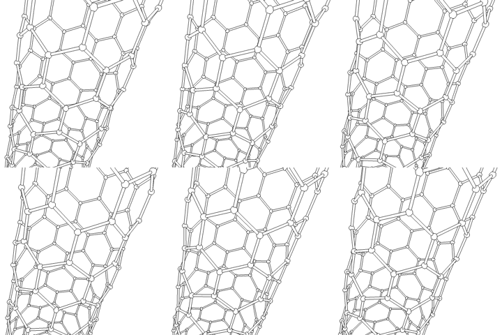
Rotating single-walled zigzag carbon nanotube

Carbon nanotubes (CNTs) are allotropes of carbon with a cylindrical nanostructure. These cylindrical carbon molecules have unusual properties, which are valuable for nanotechnology, electronics, optics and other fields of materials science and technology. Owing to the material's exceptional strength and stiffness, nanotubes have been constructed with length-to-diameter ratio of up to 132,000,000:1,[1] significantly larger than for any other material.

In addition, owing to their extraordinary thermal conductivity, mechanical, and electrical properties, carbon nanotubes find applications as additives to various structural materials. For instance, nanotubes form a tiny portion of the material(s) in some (primarily carbon fiber) baseball bats, golf clubs, car parts or damascus steel.[2][3]

Nanotubes are members of the fullerene structural family. Their name is derived from their long, hollow structure with the walls formed by one-atom-thick sheets of carbon, called graphene. These sheets are rolled at specific and discrete ("chiral") angles, and the combination of the rolling angle and radius decides the nanotube properties; for example, whether the individual nanotube shell is a metal or semiconductor. Nanotubes are categorized as single-walled nanotubes (SWNTs) and multi-walled nanotubes (MWNTs). Individual nanotubes naturally align themselves into "ropes" held together by van der Waals forces, more specifically, pi-stacking.

Applied quantum chemistry, specifically, orbital hybridization best describes chemical bonding in nanotubes. The chemical bonding of nanotubes involves entirely sp2-hybrid carbon atoms. These bonds, which are similar to those of graphite and stronger than those found in alkanes and diamond (which employ sp3-hybrid carbon atoms), provide nanotubes with their unique strength.

Types of carbon nanotubes and related structures

There is no consensus on some terms describing carbon nanotubes in scientific literature: both "-wall" and "-walled" are being used in combination with "single", "double", "triple" or "multi", and the letter C is often omitted in the abbreviation; for example, multi-walled carbon nanotube (MWNT).

Single-walled


The (n,m) nanotube naming scheme can be thought of as a vector (Ch) in an infinite graphene sheet that describes how to "roll up" the graphene sheet to make the nanotube. T denotes the tube axis, and a1 and a2 are the unit vectors of graphene in real space.

A scanning tunneling microscopy image of single-walled carbon nanotube

A transmission electron microscopy image of a single-walled carbon nanotube
d={\frac {a}{\pi }}{\sqrt {(n^{2}+nm+m^{2})}}=78.3{\sqrt {((n+m)^{2}-nm)}}{\rm {pm,}}
where a = 0.246 nm.

SWNTs are an important variety of carbon nanotube because most of their properties change significantly with the (n,m) values, and this dependence is non-monotonic (see Kataura plot). In particular, their band gap can vary from zero to about 2 eV and their electrical conductivity can show metallic or semiconducting behavior. Single-walled nanotubes are likely candidates for miniaturizing electronics. The most basic building block of these systems is the electric wire, and SWNTs with diameters of an order of a nanometer can be excellent conductors.[4][5] One useful application of SWNTs is in the development of the first intermolecular field-effect transistors (FET). The first intermolecular logic gate using SWCNT FETs was made in 2001.[6] A logic gate requires both a p-FET and an n-FET. Because SWNTs are p-FETs when exposed to oxygen and n-FETs otherwise, it is possible to expose half of an SWNT to oxygen and protect the other half from it. The resulting SWNT acts as a not logic gate with both p and n-type FETs in the same molecule.

Prices for single-walled nanotubes declined from around $1500 per gram as of 2000 to retail prices of around $50 per gram of as-produced 40–60% by weight SWNTs as of March 2010. As of 2016 the retail price of as-produced 75% by weight SWNTs were $2 per gram, cheap enough for widespread use.[7] SWNTs are forecast to make a large impact in electronics applications by 2020 according to The Global Market for Carbon Nanotubes report.

Multi-walled


A scanning electron microscopy image of carbon nanotubes bundles

Triple-walled armchair carbon nanotube

Multi-walled nanotubes (MWNTs) consist of multiple rolled layers (concentric tubes) of graphene. There are two models that can be used to describe the structures of multi-walled nanotubes. In the Russian Doll model, sheets of graphite are arranged in concentric cylinders, e.g., a (0,8) single-walled nanotube (SWNT) within a larger (0,17) single-walled nanotube. In the Parchment model, a single sheet of graphite is rolled in around itself, resembling a scroll of parchment or a rolled newspaper. The interlayer distance in multi-walled nanotubes is close to the distance between graphene layers in graphite, approximately 3.4 Å. The Russian Doll structure is observed more commonly. Its individual shells can be described as SWNTs, which can be metallic or semiconducting. Because of statistical probability and restrictions on the relative diameters of the individual tubes, one of the shells, and thus the whole MWNT, is usually a zero-gap metal.

Double-walled carbon nanotubes (DWNTs) form a special class of nanotubes because their morphology and properties are similar to those of SWNTs but they are more resistant to chemicals.[citation needed] This is especially important when it is necessary to graft chemical functions to the surface of the nanotubes (functionalization) to add properties to the CNT. Covalent functionalization of SWNTs will break some C=C double bonds, leaving "holes" in the structure on the nanotube, and thus modifying both its mechanical and electrical properties. In the case of DWNTs, only the outer wall is modified. DWNT synthesis on the gram-scale was first proposed in 2003[8] by the CCVD technique, from the selective reduction of oxide solutions in methane and hydrogen.

The telescopic motion ability of inner shells[9] and their unique mechanical properties[10] will permit the use of multi-walled nanotubes as main movable arms in coming nanomechanical devices. Retraction force that occurs to telescopic motion caused by the Lennard-Jones interaction between shells and its value is about 1.5 nN.[11]

Junctions and crosslinking


Transmission electron microscope image of carbon nanotube junction

Junctions between 2 or more nanotubes have been widely discussed theoretically.[12][13] Such junctions are quite frequently observed in samples prepared by arc discharge as well as by chemical vapor deposition. The electronic properties of such junctions were first considered theoretically by Lambin et al.,[14] who pointed out that a connection between metallic tube and a semiconducting one would represent a nanoscale heterojunction. Such a junction could therefore form a component of a nanotube-based electronic circuit. The image on the right shows a junction between two multiwalled nanotubes. Junctions between nanotubes and graphene have been considered theoretically,[15] but not widely studied experimentally. Such junctions form the basis of pillared graphene, in which parallel graphene sheets are separated by short nanotubes.[16] Pillared graphene represents a class of three-dimensional carbon nanotube architectures.


3D carbon scaffolds

Recently, several studies have highlighted the prospect of using carbon nanotubes as building blocks to fabricate three-dimensional macroscopic (>100 nm in all three dimensions) all-carbon devices. Lalwani et al. have reported a novel radical initiated thermal crosslinking method to fabricate macroscopic, free-standing, porous, all-carbon scaffolds using single- and multi-walled carbon nanotubes as building blocks.[17] These scaffolds possess macro-, micro-, and nano- structured pores and the porosity can be tailored for specific applications. These 3D all-carbon scaffolds/architectures may be used for the fabrication of the next generation of energy storage, supercapacitors, field emission transistors, high-performance catalysis, photovoltaics, and biomedical devices and implants.[18]

Other morphologies


A stable nanobud structure

Carbon nanobuds are a newly created material combining two previously discovered allotropes of carbon: carbon nanotubes and fullerenes. In this new material, fullerene-like "buds" are covalently bonded to the outer sidewalls of the underlying carbon nanotube. This hybrid material has useful properties of both fullerenes and carbon nanotubes. In particular, they have been found to be exceptionally good field emitters.[19] In composite materials, the attached fullerene molecules may function as molecular anchors preventing slipping of the nanotubes, thus improving the composite’s mechanical properties.

A carbon peapod[20][21] is a novel hybrid carbon material which traps fullerene inside a carbon nanotube. It can possess interesting magnetic properties with heating and irradiation. It can also be applied as an oscillator during theoretical investigations and predictions.[22][23]

In theory, a nanotorus is a carbon nanotube bent into a torus (doughnut shape). Nanotori are predicted to have many unique properties, such as magnetic moments 1000 times larger than previously expected for certain specific radii.[24] Properties such as magnetic moment, thermal stability, etc. vary widely depending on radius of the torus and radius of the tube.[24][25]

Graphenated carbon nanotubes are a relatively new hybrid that combines graphitic foliates grown along the sidewalls of multiwalled or bamboo style CNTs. The foliate density can vary as a function of deposition conditions (e.g. temperature and time) with their structure ranging from few layers of graphene (< 10) to thicker, more graphite-like.[26] The fundamental advantage of an integrated graphene-CNT structure is the high surface area three-dimensional framework of the CNTs coupled with the high edge density of graphene. Depositing a high density of graphene foliates along the length of aligned CNTs can significantly increase the total charge capacity per unit of nominal area as compared to other carbon nanostructures.[27]

Cup-stacked carbon nanotubes (CSCNTs) differ from other quasi-1D carbon structures, which normally behave as quasi-metallic conductors of electrons. CSCNTs exhibit semiconducting behaviors due to the stacking microstructure of graphene layers.[28]

Extreme carbon nanotubes


Cycloparaphenylene

The observation of the longest carbon nanotubes grown so far are over 1/2 m (550 mm long) was reported in 2013.[29] These nanotubes were grown on silicon substrates using an improved chemical vapor deposition (CVD) method and represent electrically uniform arrays of single-walled carbon nanotubes.[1]

The shortest carbon nanotube is the organic compound cycloparaphenylene, which was synthesized in 2008.[30]

The thinnest carbon nanotube is the armchair (2,2) CNT with a diameter of 0.3 nm. This nanotube was grown inside a multi-walled carbon nanotube. Assigning of carbon nanotube type was done by a combination of high-resolution transmission electron microscopy (HRTEM), Raman spectroscopy and density functional theory (DFT) calculations.[31]

The thinnest freestanding single-walled carbon nanotube is about 0.43 nm in diameter[32]. Researchers suggested that it can be either (5,1) or (4,2) SWCNT, but the exact type of carbon nanotube remains questionable.[33] (3,3), (4,3) and (5,1) carbon nanotubes (all about 0.4 nm in diameter) were unambiguously identified using aberration-corrected high-resolution transmission electron microscopy inside double-walled CNTs.[34]

The highest density of CNTs was achieved in 2013, grown on a conductive titanium-coated copper surface that was coated with co-catalysts cobalt and molybdenum at lower than typical temperatures of 450 °C. The tubes averaged a height of 380 nm and a mass density of 1.6 g cm−3. The material showed ohmic conductivity (lowest resistance ∼22 kΩ).[35][36]

Properties

Mechanical

Carbon nanotubes are the strongest and stiffest materials yet discovered in terms of tensile strength and elastic modulus respectively. This strength results from the covalent sp2 bonds formed between the individual carbon atoms. In 2000, a multi-walled carbon nanotube was tested to have a tensile strength of 63 gigapascals (9,100,000 psi).[37] (For illustration, this translates into the ability to endure tension of a weight equivalent to 6,422 kilograms-force (62,980 N; 14,160 lbf) on a cable with cross-section of 1 square millimetre (0.0016 sq in).) Further studies, such as one conducted in 2008, revealed that individual CNT shells have strengths of up to ≈100 gigapascals (15,000,000 psi), which is in agreement with quantum/atomistic models.[38] Since carbon nanotubes have a low density for a solid of 1.3 to 1.4 g/cm3,[39] its specific strength of up to 48,000 kN·m·kg−1 is the best of known materials, compared to high-carbon steel's 154 kN·m·kg−1.

Although the strength of individual CNT shells is extremely high, weak shear interactions between adjacent shells and tubes lead to significant reduction in the effective strength of multi-walled carbon nanotubes and carbon nanotube bundles down to only a few GPa.[40] This limitation has been recently addressed by applying high-energy electron irradiation, which crosslinks inner shells and tubes, and effectively increases the strength of these materials to ≈60 GPa for multi-walled carbon nanotubes[38] and ≈17 GPa for double-walled carbon nanotube bundles.[40] CNTs are not nearly as strong under compression. Because of their hollow structure and high aspect ratio, they tend to undergo buckling when placed under compressive, torsional, or bending stress.[41]

On the other hand, there was evidence that in the radial direction they are rather soft. The first transmission electron microscope observation of radial elasticity suggested that even the van der Waals forces can deform two adjacent nanotubes. Later, nanoindentations with atomic force microscope were performed by several groups to quantitatively measure radial elasticity of multiwalled carbon nanotubes and tapping/contact mode atomic force microscopy was also performed on single-walled carbon nanotubes. Young's modulus of on the order of several GPa showed that CNTs are in fact very soft in the radial direction.

Electrical


Band structures computed using tight binding approximation for (6,0) CNT (zigzag, metallic), (10,2) CNT (semiconducting) and (10,10) CNT (armchair, metallic).

Unlike graphene, which is a two-dimensional semimetal, carbon nanotubes are either metallic or semiconducting along the tubular axis. For a given (n,m) nanotube, if n = m, the nanotube is metallic; if nm is a multiple of 3 and n ≠ m and nm ≠ 0, then the nanotube is quasi-metallic with a very small band gap, otherwise the nanotube is a moderate semiconductor. [42] Thus all armchair (n = m) nanotubes are metallic, and nanotubes (6,4), (9,1), etc. are semiconducting.[43] Carbon nanotubes are not semimetallic because the degenerate point (that point where the π [bonding] band meets the π* [anti-bonding] band, at which the energy goes to zero) is slightly shifted away from the K point in the Brillouin zone due to the curvature of the tube surface, causing hybridization between the σ* and π* anti-bonding bands, modifying the band dispersion.

The rule regarding metallic versus semiconductor behavior has exceptions, because curvature effects in small diameter tubes can strongly influence electrical properties. Thus, a (5,0) SWCNT that should be semiconducting in fact is metallic according to the calculations. Likewise, zigzag and chiral SWCNTs with small diameters that should be metallic have a finite gap (armchair nanotubes remain metallic).[43] In theory, metallic nanotubes can carry an electric current density of 4 × 10⁹ A/cm2, which is more than 1,000 times greater than those of metals such as copper,[44] where for copper interconnects current densities are limited by electromigration. Carbon nanotubes are thus being explored as interconnects, conductivity enhancing components in composite materials and many groups are attempting to commercialize highly conducting electrical wire assembled from individual carbon nanotubes. There are significant challenges to be overcome, however, such as undesired current saturation under voltage,[45] the much more resistive nanotube-to-nanotube junctions and impurities, all of which lower the electrical conductivity of the macroscopic nanotube wires by orders of magnitude, as compared to the conductivity of the individual nanotubes.

Because of its nanoscale cross-section, electrons propagate only along the tube's axis. As a result, carbon nanotubes are frequently referred to as one-dimensional conductors. The maximum electrical conductance of a single-walled carbon nanotube is 2G0, where G0 = 2e2/h is the conductance of a single ballistic quantum channel.[46]

Due to the role of the π-electron system in determining the electronic properties of graphene, doping in carbon nanotubes differs from that of bulk crystalline semiconductors from the same group of the periodic table (e.g. silicon). Graphitic substitution of carbon atoms in the nanotube wall by boron or nitrogen dopants leads to p-type and n-type behavior, respectively, as would be expected in silicon. However, some non-substitutional (intercalated or adsorbed) dopants introduced into a carbon nanotube, such as alkali metals as well as electron-rich metallocenes, result in n-type conduction because they donate electrons to the π-electron system of the nanotube. By contrast, π-electron acceptors such as FeCl3 or electron-deficient metallocenes function as p-type dopants since they draw π-electrons away from the top of the valence band.

Intrinsic superconductivity has been reported,[47] although other experiments found no evidence of this, leaving the claim a subject of debate.[48]

Optical

Carbon nanotubes have useful absorption, photoluminescence (fluorescence), and Raman spectroscopy properties. Spectroscopic methods offer the possibility of quick and non-destructive characterization of relatively large amounts of carbon nanotubes. There is a strong demand for such characterization from the industrial point of view: numerous parameters of the nanotube synthesis can be changed, intentionally or unintentionally, to alter the nanotube quality. As shown below, optical absorption, photoluminescence and Raman spectroscopies allow quick and reliable characterization of this "nanotube quality" in terms of non-tubular carbon content, structure (chirality) of the produced nanotubes, and structural defects. Those features determine nearly any other properties such as optical, mechanical, and electrical properties.

Carbon nanotubes are unique "one-dimensional systems" which can be envisioned as rolled single sheets of graphite (or more precisely graphene). This rolling can be done at different angles and curvatures resulting in different nanotube properties. The diameter typically varies in the range 0.4–40 nm (i.e. "only" ~100 times), but the length can vary ~100,000,000,000 times, from 0.14 nm to 55.5 cm.[49] The nanotube aspect ratio, or the length-to-diameter ratio, can be as high as 132,000,000:1,[50] which is unequalled by any other material. Consequently, all the properties of the carbon nanotubes relative to those of typical semiconductors are extremely anisotropic (directionally dependent) and tunable.

Whereas mechanical, electrical and electrochemical (supercapacitor) properties of the carbon nanotubes are well established and have immediate applications, the practical use of optical properties is yet unclear. The aforementioned tunability of properties is potentially useful in optics and photonics. In particular, light-emitting diodes (LEDs)[51][52] and photo-detectors[53] based on a single nanotube have been produced in the lab. Their unique feature is not the efficiency, which is yet relatively low, but the narrow selectivity in the wavelength of emission and detection of light and the possibility of its fine tuning through the nanotube structure. In addition, bolometer[54] and optoelectronic memory[55] devices have been realised on ensembles of single-walled carbon nanotubes.

Crystallographic defects also affect the tube's electrical properties. A common result is lowered conductivity through the defective region of the tube. A defect in armchair-type tubes (which can conduct electricity) can cause the surrounding region to become semiconducting, and single monatomic vacancies induce magnetic properties.[56]

Thermal

All nanotubes are expected to be very good thermal conductors along the tube, exhibiting a property known as "ballistic conduction", but good insulators lateral to the tube axis. Measurements show that an individual SWNT has a room-temperature thermal conductivity along its axis of about 3500 W·m−1·K−1;[57] compare this to copper, a metal well known for its good thermal conductivity, which transmits 385 W·m−1·K−1. An individual SWNT has a room-temperature thermal conductivity across its axis (in the radial direction) of about 1.52 W·m−1·K−1,[58] which is about as thermally conductive as soil. Macroscopic assemblies of nanotubes such as films or fibres have reached up to 1500 W·m−1·K−1 so far.[59] The temperature stability of carbon nanotubes is estimated to be up to 2800 °C in vacuum and about 750 °C in air.[60]

Crystallographic defects strongly affect the tube's thermal properties. Such defects lead to phonon scattering, which in turn increases the relaxation rate of the phonons. This reduces the mean free path and reduces the thermal conductivity of nanotube structures. Phonon transport simulations indicate that substitutional defects such as nitrogen or boron will primarily lead to scattering of high-frequency optical phonons. However, larger-scale defects such as Stone Wales defects cause phonon scattering over a wide range of frequencies, leading to a greater reduction in thermal conductivity.[61]

Synthesis

Techniques have been developed to produce nanotubes in sizable quantities, including arc discharge, laser ablation, chemical vapor deposition (CVD) and high-pressure carbon monoxide disproportionation (HiPCO). Among these arc discharge, laser ablation, chemical vapor deposition (CVD) are batch by batch process and HiPCO is gas phase continuous process.[62] Most of these processes take place in a vacuum or with process gases. The CVD growth method is popular, as it yields high quantity and has a degree of control over diameter, length and morphology. Using particulate catalysts, large quantities of nanotubes can be synthesized by these methods, but achieving the repeatability becomes a major problem with CVD growth.[63] The HiPCO process advances in catalysis and continuous growth are making CNTs more commercially viable.[64] The HiPCO process helps in producing high purity single walled carbon nanotubes in higher quantity. The HiPCO reactor operates at high temperature 900-1100°C and high pressure ~30-50 bar.[65] It uses carbon monoxide as the carbon source and Nickel/ iron penta carbonyl as catalyst. These catalyst acts as the nucleation site for the nanotubes to grow.[62]

Vertically aligned carbon nanotube arrays are also grown by thermal chemical vapor deposition. A substrate (quartz, silicon, stainless steel, etc.) is coated with a catalytic metal (Fe, Co, Ni) layer. Typically that layer is iron, and is deposited via sputtering to a thickness of 1–5 nm. A 10–50 nm underlayer of alumina is often also put down on the substrate first. This imparts controllable wetting and good interfacial properties. When the substrate is heated to the growth temperature (~700 °C), the continuous iron film breaks up into small islands… each island then nucleates a carbon nanotube. The sputtered thickness controls the island size, and this in turn determines the nanotube diameter. Thinner iron layers drive down the diameter of the islands, and they drive down the diameter of the nanotubes grown. The amount of time that the metal island can sit at the growth temperature is limited, as they are mobile, and can merge into larger (but fewer) islands. Annealing at the growth temperature reduces the site density (number of CNT/mm2) while increasing the catalyst diameter.

The as-prepared carbon nanotubes always have impurities such as other forms of carbon (amorphous carbon, fullerene, etc.) and non-carbonaceous impurities (metal pes used for catalyst).[66][67] These impurities need to be removed to make use of the carbon nanotubes in applications.[68]

Metrology

There are many metrology standards and reference materials available for carbon nanotubes.[69]
For single-wall carbon nanotubes, ISO/TS 10868 describes a measurement method for the diameter, purity, and fraction of metallic nanotubes through optical absorption spectroscopy,[70] while ISO/TS 10797 and ISO/TS 10798 establish methods to characterize the morphology and elemental composition of single-wall carbon nanotubes, using transmission electron microscopy and scanning electron microscopy respectively, coupled with energy dispersive X-ray spectrometry analysis.[71][72]
NIST SRM 2483 is a soot of single-wall carbon nanotubes used as a reference material for elemental analysis, and was characterized using thermogravimetric analysis, prompt gamma activation analysis, induced neutron activation analysis, inductively coupled plasma mass spectroscopy, resonant Raman scattering, UV-visible-near infrared fluorescence spectroscopy and absorption spectroscopy, scanning electron microscopy, and transmission electron microscopy.[73][74] The Canadian National Research Council also offers a certified reference material SWCNT-1 for elemental analysis using neutron activation analysis and inductively coupled plasma mass spectroscopy.[69][75] NIST RM 8281 is a mixture of three lengths of single-wall carbon nanotube.[73][76]

For multiwall carbon nanotubes, ISO/TR 10929 identifies the basic properties and the content of impurities,[77] while ISO/TS 11888 describes morphology using scanning electron microscopy, transmission electron microscopy, viscometry, and light scattering analysis.[78] ISO/TS 10798 is also valid for multiwall carbon nanotubes.[72]

Chemical modification

Carbon nanotubes can be functionalized to attain desired properties that can be used in a wide variety of applications. The two main methods of carbon nanotube functionalization are covalent and non-covalent modifications. Because of their hydrophobic nature, carbon nanotubes tend to agglomerate hindering their dispersion in solvents or viscous polymer melts. The resulting nanotube bundles or aggregates reduce the mechanical performance of the final composite. The surface of the carbon nanotubes can be modified to reduce the hydrophobicity and improve interfacial adhesion to a bulk polymer through chemical attachment.[79]

Applications

Current

Current use and application of nanotubes has mostly been limited to the use of bulk nanotubes, which is a mass of rather unorganized fragments of nanotubes. Bulk nanotube materials may never achieve a tensile strength similar to that of individual tubes, but such composites may, nevertheless, yield strengths sufficient for many applications. Bulk carbon nanotubes have already been used as composite fibers in polymers to improve the mechanical, thermal and electrical properties of the bulk product.
  • Easton-Bell Sports, Inc. have been in partnership with Zyvex Performance Materials, using CNT technology in a number of their bicycle components – including flat and riser handlebars, cranks, forks, seatposts, stems and aero bars.
  • Zyvex Technologies has also built a 54' maritime vessel, the Piranha Unmanned Surface Vessel, as a technology demonstrator for what is possible using CNT technology. CNTs help improve the structural performance of the vessel, resulting in a lightweight 8,000 lb boat that can carry a payload of 15,000 lb over a range of 2,500 miles.[80]
  • Amroy Europe Oy manufactures Hybtonite carbon nanoepoxy resins where carbon nanotubes have been chemically activated to bond to epoxy, resulting in a composite material that is 20% to 30% stronger than other composite materials. It has been used for wind turbines, marine paints and a variety of sports gear such as skis, ice hockey sticks, baseball bats, hunting arrows, and surfboards.[81]
  • The Boeing Company has patented the use of carbon nanotubes for structural health monitoring[82] of composites used in aircraft structures. This technology will greatly reduce the risk of an in-flight failure caused by structural degradation of aircraft.
Other current applications include:
Current research for modern applications include:
  • using carbon nanotubes as a scaffold for diverse microfabrication techniques.[85]
  • energy dissipation in self-organized nanostructures under influence of an electric field.[86]
  • using carbon nanotubes for environmental monitoring due to their active surface area and their ability to absorb gases.[87]

Potential

The strength and flexibility of carbon nanotubes makes them of potential use in controlling other nanoscale structures, which suggests they will have an important role in nanotechnology engineering. The highest tensile strength of an individual multi-walled carbon nanotube has been tested to be 63 GPa.[37] Carbon nanotubes were found in Damascus steel from the 17th century, possibly helping to account for the legendary strength of the swords made of it.[88][89] Recently, several studies have highlighted the prospect of using carbon nanotubes as building blocks to fabricate three-dimensional macroscopic (>1mm in all three dimensions) all-carbon devices. Lalwani et al. have reported a novel radical initiated thermal crosslinking method to fabricated macroscopic, free-standing, porous, all-carbon scaffolds using single- and multi-walled carbon nanotubes as building blocks.[17] These scaffolds possess macro-, micro-, and nano- structured pores and the porosity can be tailored for specific applications. These 3D all-carbon scaffolds/architectures may be used for the fabrication of the next generation of energy storage, supercapacitors, field emission transistors, high-performance catalysis,[90] photovoltaics, and biomedical devices and implants.

CNTs are potential candidates for future via and wire material in nano-scale VLSI circuits. Eliminating electromigration reliability concerns that plague todays Cu interconnects, isolated (single and multi-wall) CNTs can carry current densities in excess of 1000 MA/sq-cm without electromigration damage.[91]

Large quantities of pure CNTs can be made into a freestanding sheet or film by surface-engineered tape-casting (SETC) fabrication technique which is a scalable method to fabricate flexible and foldable sheets with superior properties.[92][93] Another reported form factor is CNT fiber (a.k.a. filament) by wet spinning.[94] The fiber is either directly spun from the synthesis pot or spun from pre-made dissolved CNTs. Individual fibers can be turned into a yarn. Apart from its strength and flexibility, the main advantage is making an electrically conducting yarn. The electronic properties of individual CNT fibers (i.e. bundle of individual CNT) are governed by the two-dimensional structure of CNTs. The fibers were measured to have a resistivity only one order of magnitude higher than metallic conductors at 300K. By further optimizing the CNTs and CNT fibers, CNT fibers with improved electrical properties could be developed.[91][95]

CNT-based yarns are suitable for applications in energy and electrochemical water treatment when coated with an ion-exchange membrane.[96] Also, CNT-based yarns could replace copper as a winding material. Pyrhönen et al. (2015) have built a motor using CNT winding.[97][98]

Safety and health

The National Institute for Occupational Safety and Health (NIOSH) is the leading United States federal agency conducting research and providing guidance on the occupational safety and health implications and applications of nanotechnology. Early scientific studies have indicated that some of these nanoscale particles may pose a greater health risk than the larger bulk form of these materials. In 2013, NIOSH published a Current Intelligence Bulletin detailing the potential hazards and recommended exposure limit for carbon nanotubes and fibers.[99]

As of October 2016, single wall carbon nanotubes have been registered through the European Union's Registration, Evaluation, Authorization and Restriction of Chemicals (REACH) regulations, based on evaluation of the potentially hazardous properties of SWCNT. Based on this registration, SWCNT commercialization is allowed in the EU up to 10 metric tons. Currently, the type of SWCNT registered through REACH is limited to the specific type of single wall carbon nanotubes manufactured by OCSiAl, which submitted the application.[100]

History

The true identity of the discoverers of carbon nanotubes is a subject of some controversy.[101] A 2006 editorial written by Marc Monthioux and Vladimir Kuznetsov in the journal Carbon described the interesting and often-misstated origin of the carbon nanotube.[102] A large percentage of academic and popular literature attributes the discovery of hollow, nanometer-size tubes composed of graphitic carbon to Sumio Iijima of NEC in 1991. He published a paper describing his discovery which initiated a flurry of excitement and could be credited by inspiring the many scientists now studying applications of carbon nanotubes. Though Iijima has been given much of the credit for discovering carbon nanotubes, it turns out that the timeline of carbon nanotubes goes back much further than 1991.[101]

In 1952, L. V. Radushkevich and V. M. Lukyanovich published clear images of 50 nanometer diameter tubes made of carbon in the Soviet Journal of Physical Chemistry.[103] This discovery was largely unnoticed, as the article was published in Russian, and Western scientists' access to Soviet press was limited during the Cold War. Monthioux and Kuznetsov mentioned in their Carbon editorial:[102]
The fact is, Radushkevich and Lukyanovich [..] should be credited for the discovery that carbon filaments could be hollow and have a nanometer- size diameter, that is to say for the discovery of carbon nanotubes.
In 1976, Morinobu Endo of CNRS observed hollow tubes of rolled up graphite sheets synthesised by a chemical vapour-growth technique.[104] The first specimens observed would later come to be known as single-walled carbon nanotubes (SWNTs).[105] Endo, in his early review of vapor-phase-grown carbon fibers (VPCF), also reminded us that he had observed a hollow tube, linearly extended with parallel carbon layer faces near the fiber core.[106] This appears to be the observation of multi-walled carbon nanotubes at the center of the fiber.[105] The mass-produced MWCNTs today are strongly related to the VPGCF developed by Endo.[105] In fact, they call it the “Endo-process”, out of respect for his early work and patents.[105][107]

In 1979, John Abrahamson presented evidence of carbon nanotubes at the 14th Biennial Conference of Carbon at Pennsylvania State University. The conference paper described carbon nanotubes as carbon fibers that were produced on carbon anodes during arc discharge. A characterization of these fibers was given as well as hypotheses for their growth in a nitrogen atmosphere at low pressures.[108]

In 1981, a group of Soviet scientists published the results of chemical and structural characterization of carbon nanoparticles produced by a thermocatalytical disproportionation of carbon monoxide. Using TEM images and XRD patterns, the authors suggested that their “carbon multi-layer tubular crystals” were formed by rolling graphene layers into cylinders. They speculated that by rolling graphene layers into a cylinder, many different arrangements of graphene hexagonal nets are possible. They suggested two possibilities of such arrangements: circular arrangement (armchair nanotube) and a spiral, helical arrangement (chiral tube).[109]

In 1987, Howard G. Tennent of Hyperion Catalysis was issued a U.S. patent for the production of "cylindrical discrete carbon fibrils" with a "constant diameter between about 3.5 and about 70 nanometers..., length 102 times the diameter, and an outer region of multiple essentially continuous layers of ordered carbon atoms and a distinct inner core...."[110]

Iijima's discovery of multi-walled carbon nanotubes in the insoluble material of arc-burned graphite rods in 1991[111] and Mintmire, Dunlap, and White's independent prediction that if single-walled carbon nanotubes could be made, then they would exhibit remarkable conducting properties[112] helped create the initial buzz that is now associated with carbon nanotubes. Nanotube research accelerated greatly following the independent discoveries[113][114] by Bethune at IBM and Iijima at NEC of single-walled carbon nanotubes and methods to specifically produce them by adding transition-metal catalysts to the carbon in an arc discharge. The arc discharge technique was well-known to produce the famed Buckminster fullerene on a preparative scale,[115] and these results appeared to extend the run of accidental discoveries relating to fullerenes. The discovery of nanotubes remains a contentious issue. Many believe that Iijima's report in 1991 is of particular importance because it brought carbon nanotubes into the awareness of the scientific community as a whole.[101][105]

United States labor law

From Wikipedia, the free encyclopedia https://en.wikipedia.org/wiki/Uni...