From Wikipedia, the free encyclopedia
A
semiconductor material has an
electrical conductivity value falling between that of a
conductor – such as copper, gold etc. – and an
insulator, such as glass. Their
resistance
decreases as their temperature increases, which is behaviour opposite
to that of a metal. Their conducting properties may be altered in useful
ways by the deliberate, controlled introduction of impurities ("
doping") into the
crystal structure. Where two differently-doped regions exist in the same crystal, a
semiconductor junction is created. The behavior of
charge carriers which include
electrons,
ions and
electron holes at these junctions is the basis of
diodes,
transistors and all modern electronics.
Semiconductor devices
can display a range of useful properties such as passing current more
easily in one direction than the other, showing variable resistance, and
sensitivity to light or heat. Because the electrical properties of a
semiconductor material can be modified by doping, or by the application
of electrical fields or light, devices made from semiconductors can be
used for amplification, switching, and
energy conversion.
The
conductivity of
silicon
is increased by adding a small amount of pentavalent (antimony,
phosphorus, or arsenic) or trivalent (boron, gallium, indium) atoms (~
part in 10
8). This process is known as doping and resulting semiconductors are known as doped or extrinsic semiconductors.
The modern understanding of the properties of a semiconductor relies on
quantum physics to explain the movement of charge carriers in a
crystal lattice.
[1]
Doping greatly increases the number of charge carriers within the
crystal. When a doped semiconductor contains mostly free holes it is
called "
p-type", and when it contains mostly free electrons it is known as "
n-type".
The semiconductor materials used in electronic devices are doped under
precise conditions to control the concentration and regions of p- and
n-type dopants. A single semiconductor crystal can have many p- and
n-type regions; the
p–n junctions between these regions are responsible for the useful electronic behavior.
Although some pure elements and many compounds display semiconductor properties,
silicon,
[2][better source needed] germanium, and compounds of
gallium are the most widely used in electronic devices. Elements near the so-called "
metalloid staircase", where the metalloids are located on the periodic table, are usually used as semiconductors.
Some of the properties of semiconductor materials were observed
throughout the mid 19th and first decades of the 20th century. The first
practical application of semiconductors in electronics was the 1904
development of the
cat's-whisker detector,
a primitive semiconductor diode widely used in early radio receivers.
Developments in quantum physics in turn allowed the development of the
transistor in 1947
[3] and the
integrated circuit in 1958.
Properties
- Variable conductivity
- Semiconductors in their natural state are poor conductors because a current requires the flow of electrons, and semiconductors have their valence bands
filled, preventing the entry flow of new electrons. There are several
developed techniques that allow semiconducting materials to behave like
conducting materials, such as doping or gating.
These modifications have two outcomes: n-type and p-type. These refer
to the excess or shortage of electrons, respectively. An unbalanced
number of electrons would cause a current to flow through the material.[4]
- Heterojunctions
- Heterojunctions
occur when two differently doped semiconducting materials are joined
together. For example, a configuration could consist of p-doped and
n-doped germanium.
This results in an exchange of electrons and holes between the
differently doped semiconducting materials. The n-doped germanium would
have an excess of electrons, and the p-doped germanium would have an
excess of holes. The transfer occurs until equilibrium is reached by a
process called recombination,
which causes the migrating electrons from the n-type to come in contact
with the migrating holes from the p-type. A product of this process is
charged ions, which result in an electric field.[1][4]
- Excited electrons
- A difference in electric potential on a semiconducting material
would cause it to leave thermal equilibrium and create a non-equilibrium
situation. This introduces electrons and holes to the system, which
interact via a process called ambipolar diffusion.
Whenever thermal equilibrium is disturbed in a semiconducting material,
the number of holes and electrons changes. Such disruptions can occur
as a result of a temperature difference or photons,
which can enter the system and create electrons and holes. The process
that creates and annihilates electrons and holes are called generation and recombination.[4]
- Light emission
- In certain semiconductors, excited electrons can relax by emitting light instead of producing heat.[5] These semiconductors are used in the construction of light-emitting diodes and fluorescent quantum dots.
- Thermal energy conversion
- Semiconductors have large thermoelectric power factors making them useful in thermoelectric generators, as well as high thermoelectric figures of merit making them useful in thermoelectric coolers.[6]
Materials
A large number of elements and compounds have semiconducting properties, including:
[7]
- Certain pure elements are found in Group 14 of the periodic table; the most commercially important of these elements are silicon and germanium.
Silicon and germanium are used here effectively because they have 4
valence electrons in their outermost shell which gives them the ability
to gain or lose electrons equally at the same time.
- Binary compounds, particularly between elements in Groups 13 and 15, such as gallium arsenide, Groups 12 and 16, groups 14 and 16, and between different group 14 elements, e.g. silicon carbide.
- Certain ternary compounds, oxides and alloys.
- Organic semiconductors, made of organic compounds.
Most common semiconducting materials are crystalline solids, but
amorphous and liquid semiconductors are also known. These include
hydrogenated amorphous silicon and mixtures of
arsenic,
selenium and
tellurium
in a variety of proportions. These compounds share with better known
semiconductors the properties of intermediate conductivity and a rapid
variation of conductivity with temperature, as well as occasional
negative resistance.
Such disordered materials lack the rigid crystalline structure of
conventional semiconductors such as silicon. They are generally used in
thin film
structures, which do not require material of higher electronic quality,
being relatively insensitive to impurities and radiation damage.
Preparation of semiconductor materials
Almost all of today's electronic technology involves the use of semiconductors, with the most important aspect being the
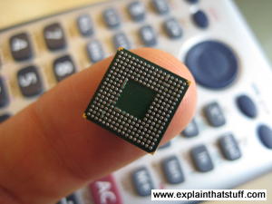
integrated circuit (IC), which are found in
laptops, scanners,
cell-phones,
etc. Semiconductors for ICs are mass-produced. To create an ideal
semiconducting material, chemical purity is paramount. Any small
imperfection can have a drastic effect on how the semiconducting
material behaves due to the scale at which the materials are used.
[4]
A high degree of crystalline perfection is also required, since faults in crystal structure (such as
dislocations,
twins, and
stacking faults)
interfere with the semiconducting properties of the material.
Crystalline faults are a major cause of defective semiconductor devices.
The larger the crystal, the more difficult it is to achieve the
necessary perfection. Current mass production processes use crystal
ingots between 100 and 300 mm (3.9 and 11.8 in) in diameter which are grown as cylinders and sliced into
wafers.
There is a combination of processes that is used to prepare semiconducting materials for ICs. One process is called
thermal oxidation, which forms
silicon dioxide on the surface of the
silicon. This is used as a
gate insulator and
field oxide. Other processes are called
photomasks and
photolithography. This process is what creates the patterns on the circuity in the integrated circuit.
Ultraviolet light is used along with a
photoresist layer to create a chemical change that generates the patterns for the circuit.
[4]
Etching is the next process that is required. The part of the silicon that was not covered by the
photoresist layer from the previous step can now be etched. The main process typically used today is called
plasma etching. Plasma etching usually involves an
etch gas pumped in a low-pressure chamber to create
plasma. A common etch gas is
chlorofluorocarbon, or more commonly known
Freon. A high
radio-frequency voltage between the
cathode and
anode is what creates the plasma in the chamber. The
silicon wafer
is located on the cathode, which causes it to be hit by the positively
charged ions that are released from the plasma. The end result is
silicon that is etched
anisotropically.
[1][4]
The last process is called
diffusion. This is the process that gives the semiconducting material its desired semiconducting properties. It is also known as
doping. The process introduces an impure atom to the system, which creates the
p-n junction.
In order to get the impure atoms embedded in the silicon wafer, the
wafer is first put in a 1,100 degree Celsius chamber. The atoms are
injected in and eventually diffuse with the silicon. After the process
is completed and the silicon has reached room temperature, the doping
process is done and the semiconducting material is ready to be used in
an integrated circuit.
[1][4]
Physics of semiconductors
Energy bands and electrical conduction
Semiconductors are defined by their unique electric conductive behavior, somewhere between that of a conductor and an insulator.
[8]
The differences between these materials can be understood in terms of the
quantum states for electrons, each of which may contain zero or one electron (by the
Pauli exclusion principle). These states are associated with the
electronic band structure of the material.
Electrical conductivity arises due to the presence of electrons in states that are
delocalized (extending through the material), however in order to transport electrons a state must be
partially filled, containing an electron only part of the time.
[9] If the state is always occupied with an electron, then it is inert, blocking the passage of other electrons via that state.
The energies of these quantum states are critical, since a state is partially filled only if its energy is near the
Fermi level (see
Fermi–Dirac statistics).
High conductivity in a material comes from it having many partially filled states and much state delocalization.
Metals are good
electrical conductors and have many partially filled states with energies near their Fermi level.
Insulators, by contrast, have few partially filled states, their Fermi levels sit within
band gaps
with few energy states to occupy.
Importantly, an insulator can be made to conduct by increasing its
temperature: heating provides energy to promote some electrons across
the band gap, inducing partially filled states in both the band of
states beneath the band gap (
valence band) and the band of states above the band gap (
conduction band).
An (intrinsic) semiconductor has a band gap that is smaller than that of
an insulator and at room temperature significant numbers of electrons
can be excited to cross the band gap.
[10]
A pure semiconductor, however, is not very useful, as it is neither a very good insulator nor a very good conductor.
However, one important feature of semiconductors (and some insulators, known as
semi-insulators) is that their conductivity can be increased and controlled by
doping with impurities and
gating
with electric fields. Doping and gating move either the conduction or
valence band much closer to the Fermi level, and greatly increase the
number of partially filled states.
Some wider-
band gap semiconductor materials are sometimes referred to as
semi-insulators.
When undoped, these have electrical conductivity nearer to that of
electrical insulators, however they can be doped (making them as useful
as semiconductors). Semi-insulators find niche applications in
micro-electronics, such as substrates for
HEMT. An example of a common semi-insulator is
gallium arsenide.
[11] Some materials, such as
titanium dioxide,
can even be used as insulating materials for some applications, while
being treated as wide-gap semiconductors for other applications.
Charge carriers (electrons and holes)
The partial filling of the states at the bottom of the conduction band can be understood as adding electrons to that band.
The electrons do not stay indefinitely (due to the natural thermal
recombination)
but they can move around for some time.
The actual concentration of electrons is typically very dilute, and so
(unlike in metals) it is possible to think of the electrons in the
conduction band of a semiconductor as a sort of classical
ideal gas, where the electrons fly around freely without being subject to the
Pauli exclusion principle. In most semiconductors the conduction bands have a parabolic
dispersion relation,
and so these electrons respond to forces (electric field, magnetic
field, etc.) much like they would in a vacuum, though with a different
effective mass.
[10]
Because the electrons behave like an ideal gas, one may also think about conduction in very simplistic terms such as the
Drude model, and introduce concepts such as
electron mobility.
For partial filling at the top of the valence band, it is helpful to introduce the concept of an
electron hole.
Although the electrons in the valence band are always moving around, a
completely full valence band is inert, not conducting any current.
If an electron is taken out of the valence band, then the trajectory
that the electron would normally have taken is now missing its charge.
For the purposes of electric current, this combination of the full
valence band, minus the electron, can be converted into a picture of a
completely empty band containing a positively charged particle that
moves in the same way as the electron.
Combined with the
negative effective mass of the electrons at the
top of the valence band, we arrive at a picture of a positively charged
particle that responds to electric and magnetic fields just as a normal
positively charged particle would do in vacuum, again with some
positive effective mass.
[10]
This particle is called a hole, and the collection of holes in the
valence band can again be understood in simple classical terms (as with
the electrons in the conduction band).
Carrier generation and recombination
When
ionizing radiation
strikes a semiconductor, it may excite an electron out of its energy
level and consequently leave a hole. This process is known as
electron–hole pair generation. Electron-hole pairs are constantly generated from
thermal energy as well, in the absence of any external energy source.
Electron-hole pairs are also apt to recombine.
Conservation of energy demands that these recombination events, in which an electron loses an amount of
energy larger than the
band gap, be accompanied by the emission of thermal energy (in the form of
phonons) or radiation (in the form of
photons).
In some states, the generation and recombination of electron–hole
pairs are in equipoise. The number of electron-hole pairs in the
steady state at a given temperature is determined by
quantum statistical mechanics. The precise
quantum mechanical mechanisms of generation and recombination are governed by
conservation of energy and
conservation of momentum.
As the probability that electrons and holes meet together is
proportional to the product of their numbers, the product is in steady
state nearly constant at a given temperature, providing that there is no
significant electric field (which might "flush" carriers of both types,
or move them from neighbour regions containing more of them to meet
together) or externally driven pair generation. The product is a
function of the temperature, as the probability of getting enough
thermal energy to produce a pair increases with temperature, being
approximately exp(−
EG/
kT), where
k is
Boltzmann's constant,
T is absolute temperature and
EG is band gap.
The probability of meeting is increased by carrier
traps—impurities or dislocations which can trap an electron or hole and
hold it until a pair is completed. Such carrier traps are sometimes
purposely added to reduce the time needed to reach the steady state.
[12]
Doping
The conductivity of semiconductors may easily be modified by introducing impurities into their
crystal lattice. The process of adding controlled impurities to a semiconductor is known as
doping. The amount of impurity, or dopant, added to an
intrinsic (pure) semiconductor varies its level of conductivity. Doped semiconductors are referred to as
extrinsic. By adding impurity to the pure semiconductors, the electrical conductivity may be varied by factors of thousands or millions.
A 1 cm
3 specimen of a metal or semiconductor has of the order of 10
22 atoms. In a metal, every atom donates at least one free electron for conduction, thus 1 cm
3 of metal contains on the order of 10
22 free electrons, whereas a 1 cm
3 sample of pure germanium at 20 °C contains about
4.2×10²² atoms, but only
2.5×10¹³ free electrons and
2.5×10¹³ holes. The addition of 0.001% of arsenic (an impurity) donates an extra 10
17 free electrons in the same volume and the electrical conductivity is increased by a factor of 10,000.
The materials chosen as suitable dopants depend on the atomic
properties of both the dopant and the material to be doped. In general,
dopants that produce the desired controlled changes are classified as
either electron
acceptors or
donors. Semiconductors doped with
donor impurities are called
n-type, while those doped with
acceptor impurities are known as
p-type. The n and p type designations indicate which charge carrier acts as the material's
majority carrier. The opposite carrier is called the
minority carrier, which exists due to thermal excitation at a much lower concentration compared to the majority carrier.
For example, the pure semiconductor
silicon has four valence electrons which bond each silicon atom to its neighbors. In silicon, the most common dopants are
group III and
group V
elements. Group III elements all contain three valence electrons,
causing them to function as acceptors when used to dope silicon. When an
acceptor atom replaces a silicon atom in the crystal, a vacant state
(an electron "hole") is created, which can move around the lattice and
functions as a charge carrier. Group V elements have five valence
electrons, which allows them to act as a donor; substitution of these
atoms for silicon creates an extra free electron. Therefore, a silicon
crystal doped with
boron creates a p-type semiconductor whereas one doped with
phosphorus results in an n-type material.
During
manufacture, dopants can be diffused into the semiconductor body by contact with gaseous compounds of the desired element, or
ion implantation can be used to accurately position the doped regions.
Early history of semiconductors
The history of the understanding of semiconductors begins with
experiments on the electrical properties of materials. The properties of
negative temperature coefficient of resistance, rectification, and
light-sensitivity were observed starting in the early 19th century.
Thomas Johann Seebeck was the first to notice an
effect due to semiconductors, in 1821.
[13] In 1833,
Michael Faraday reported that the resistance of specimens of
silver sulfide decreases when they are heated. This is contrary to the behavior of metallic substances such as copper. In 1839,
Alexandre Edmond Becquerel reported observation of a voltage between a solid and a liquid electrolyte when struck by light, the
photovoltaic effect. In 1873
Willoughby Smith observed that
selenium resistors exhibit decreasing resistance when light falls on them. In 1874
Karl Ferdinand Braun observed conduction and
rectification in metallic
sulfides, although this effect had been discovered much earlier by Peter Munck af Rosenschold (
sv) writing for the Annalen der Physik und Chemie in 1835,
[14] and
Arthur Schuster found that a copper oxide layer on wires has rectification properties that ceases when the wires are cleaned.
William Grylls Adams and
Richard Evans Day observed the photovoltaic effect in selenium in 1876.
[15]
A unified explanation of these phenomena required a theory of
solid-state physics which developed greatly in the first half of the 20th Century. In 1878
Edwin Herbert Hall demonstrated the deflection of flowing charge carriers by an applied magnetic field, the
Hall effect. The discovery of the
electron by
J.J. Thomson in 1897 prompted theories of electron-based conduction in solids.
Karl Baedeker,
by observing a Hall effect with the reverse sign to that in metals,
theorized that copper iodide had positive charge carriers.
Johan Koenigsberger
classified solid materials as metals, insulators and "variable
conductors" in 1914 although his student Josef Weiss already introduced
the term
Halbleiter (semiconductor in modern meaning) in PhD thesis in 1910.
[16][17] Felix Bloch
published a theory of the movement of electrons through atomic lattices
in 1928. In 1930, B. Gudden stated that conductivity in semiconductors
was due to minor concentrations of impurities. By 1931, the band theory
of conduction had been established by
Alan Herries Wilson and the concept of band gaps had been developed.
Walter H. Schottky and
Nevill Francis Mott developed models of the potential barrier and of the characteristics of a
metal-semiconductor junction. By 1938,
Boris Davydov had developed a theory of the copper-oxide rectifier, identifying the effect of the
p–n junction and the importance of minority carriers and surface states.
[18]
Agreement between theoretical predictions (based on developing
quantum mechanics) and experimental results was sometimes poor. This was
later explained by
John Bardeen
as due to the extreme "structure sensitive" behavior of semiconductors,
whose properties change dramatically based on tiny amounts of
impurities.
[18]
Commercially pure materials of the 1920s containing varying proportions
of trace contaminants produced differing experimental results. This
spurred the development of improved material refining techniques,
culminating in modern semiconductor refineries producing materials with
parts-per-trillion purity.
Devices using semiconductors were at first constructed based on
empirical knowledge, before semiconductor theory provided a guide to
construction of more capable and reliable devices.
Alexander Graham Bell used the light-sensitive property of selenium to
transmit sound over a beam of light in 1880. A working solar cell, of low efficiency, was constructed by
Charles Fritts
in 1883 using a metal plate coated with selenium and a thin layer of
gold; the device became commercially useful in photographic light meters
in the 1930s.
[18] Point-contact microwave detector rectifiers made of lead sulfide were used by
Jagadish Chandra Bose in 1904; the
cat's-whisker detector using natural galena or other materials became a common device in the
development of radio. However, it was somewhat unpredictable in operation and required manual adjustment for best performance. In 1906
H.J. Round observed light emission when electric current passed through silicon carbide crystals, the principle behind the
light-emitting diode.
Oleg Losev
observed similar light emission in 1922 but at the time the effect had
no practical use. Power rectifiers, using copper oxide and selenium,
were developed in the 1920s and became commercially important as an
alternative to
vacuum tube rectifiers.
[15][18]
In the years preceding World War II, infra-red detection and
communications devices prompted research into lead-sulfide and
lead-selenide materials. These devices were used for detecting ships and
aircraft, for infrared rangefinders, and for voice communication
systems. The point-contact crystal detector became vital for microwave
radio systems, since available vacuum tube devices could not serve as
detectors above about 4000 MHz; advanced radar systems relied on the
fast response of crystal detectors. Considerable research and
development of silicon materials occurred during the war to develop
detectors of consistent quality.
[18]
Detector and power rectifiers could not amplify a signal. Many
efforts were made to develop a solid-state amplifier and were successful
in developing a device called the point contact transistor which could
amplify 20db or more.
[18] In 1922
Oleg Losev developed two-terminal,
negative resistance amplifiers for radio, and he perished in the
Siege of Leningrad after successful completion. In 1926
Julius Edgar Lilienfeld
patented a device resembling a modern field-effect transistor, but it
was not practical. R. Hilsch and R. W. Pohl in 1938 demonstrated a
solid-state amplifier using a structure resembling the control grid of a
vacuum tube; although the device displayed power gain, it had a
cut-off frequency of one cycle per second, too low for any practical applications, but an effective application of the available theory.
[18] At
Bell Labs,
William Shockley and A. Holden started investigating solid-state amplifiers in 1938. The first p–n junction in silicon was observed by
Russell Ohl
about 1941, when a specimen was found to be light-sensitive, with a
sharp boundary between p-type impurity at one end and n-type at the
other. A slice cut from the specimen at the p–n boundary developed a
voltage when exposed to light.
In France, during the war,
Herbert Mataré had observed amplification between adjacent point contacts on a germanium base. After the war, Mataré's group announced their "
Transistron" amplifier only shortly after Bell Labs announced the "
transistor".