Search This Blog

Wednesday, April 10, 2019

Network theory

From Wikipedia, the free encyclopedia

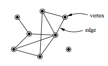
A small example network with eight vertices and ten edges
 
Network theory is the study of graphs as a representation of either symmetric relations or asymmetric relations between discrete objects. In computer science and network science, network theory is a part of graph theory: a network can be defined as a graph in which nodes and/or edges have attributes (e.g. names). 

Network theory has applications in many disciplines including statistical physics, particle physics, computer science, electrical engineering, biology, economics, finance, operations research, climatology, ecology and sociology. Applications of network theory include logistical networks, the World Wide Web, Internet, gene regulatory networks, metabolic networks, social networks, epistemological networks, etc.; see List of network theory topics for more examples. 

Euler's solution of the Seven Bridges of Königsberg problem is considered to be the first true proof in the theory of networks.

Network optimization

Network Optimization
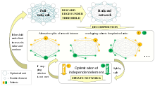
Break down a NP-hard network optimization task into subtasks by discarding of the most irrelevant interactions in network.
 
Network problems that involve finding an optimal way of doing something are studied under the name combinatorial optimization. Examples include network flow, shortest path problem, transport problem, transshipment problem, location problem, matching problem, assignment problem, packing problem, routing problem, critical path analysis and PERT (Program Evaluation & Review Technique). In order to break a NP-hard task of network optimization down into subtasks the network is decomposed into relatively independent subnets.

Network analysis

Electric network analysis

The electric power systems analysis could be conducted using network theory from two main points of view: 

(1) an abstract perspective (i.e., as a graph consists from nodes and edges), regardless of the electric power aspects (e.g., transmission line impedances). Most of these studies focus only on the abstract structure of the power grid using node degree distribution and betweenness distribution, which introduces substantial insight regarding the vulnerability assessment of the grid. Through these types of studies, the category of the grid structure could be identified from the complex network perspective (e.g., single-scale, scale-free). This classification might help the electric power system engineers in the planning stage or while upgrading the infrastructure (e.g., add a new transmission line) to maintain a proper redundancy level in the transmission system.

(2) weighted graphs that blend an abstract understanding of complex network theories and electric power systems properties.

Social network analysis

Visualization of social network analysis
 
Social network analysis examines the structure of relationships between social entities. These entities are often persons, but may also be groups, organizations, nation states, web sites, or scholarly publications

Since the 1970s, the empirical study of networks has played a central role in social science, and many of the mathematical and statistical tools used for studying networks have been first developed in sociology. Amongst many other applications, social network analysis has been used to understand the diffusion of innovations, news and rumors. Similarly, it has been used to examine the spread of both diseases and health-related behaviors. It has also been applied to the study of markets, where it has been used to examine the role of trust in exchange relationships and of social mechanisms in setting prices. Similarly, it has been used to study recruitment into political movements and social organizations. It has also been used to conceptualize scientific disagreements as well as academic prestige. More recently, network analysis (and its close cousin traffic analysis) has gained a significant use in military intelligence, for uncovering insurgent networks of both hierarchical and leaderless nature.

Biological network analysis

With the recent explosion of publicly available high throughput biological data, the analysis of molecular networks has gained significant interest. The type of analysis in this context is closely related to social network analysis, but often focusing on local patterns in the network. For example, network motifs are small subgraphs that are over-represented in the network. Similarly, activity motifs are patterns in the attributes of nodes and edges in the network that are over-represented given the network structure. Using networks to analyse patterns in biological systems, such as food-webs, allows us to visualize the nature and strength of interactions between species. The analysis of biological networks with respect to diseases has led to the development of the field of network medicine. Recent examples of application of network theory in biology include applications to understanding the cell cycle. The interactions between physiological systems like brain, heart, eyes, etc. can be regarded as a physiological network.

Narrative network analysis

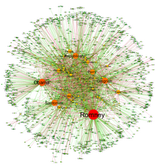
Narrative network of US Elections 2012
 
The automatic parsing of textual corpora has enabled the extraction of actors and their relational networks on a vast scale. The resulting narrative networks, which can contain thousands of nodes, are then analysed by using tools from Network theory to identify the key actors, the key communities or parties, and general properties such as robustness or structural stability of the overall network, or centrality of certain nodes. This automates the approach introduced by Quantitative Narrative Analysis, whereby subject-verb-object triplets are identified with pairs of actors linked by an action, or pairs formed by actor-object.

Link analysis

Link analysis is a subset of network analysis, exploring associations between objects. An example may be examining the addresses of suspects and victims, the telephone numbers they have dialed and financial transactions that they have partaken in during a given timeframe, and the familial relationships between these subjects as a part of police investigation. Link analysis here provides the crucial relationships and associations between very many objects of different types that are not apparent from isolated pieces of information. Computer-assisted or fully automatic computer-based link analysis is increasingly employed by banks and insurance agencies in fraud detection, by telecommunication operators in telecommunication network analysis, by medical sector in epidemiology and pharmacology, in law enforcement investigations, by search engines for relevance rating (and conversely by the spammers for spamdexing and by business owners for search engine optimization), and everywhere else where relationships between many objects have to be analyzed. Links are also derived from similarity of time behavior in both nodes. Examples include climate networks where the links between two locations (nodes) are determined for example, by the similarity of the rainfall or temperature fluctuations in both sites.

Network robustness

The structural robustness of networks is studied using percolation theory. When a critical fraction of nodes (or links) is removed the network becomes fragmented into small disconnected clusters. This phenomenon is called percolation, and it represents an order-disorder type of phase transition with critical exponents. Percolation theory can predict the size of the largest component (called giant component), the critical threshold and the critical exponents.

Web link analysis

Several Web search ranking algorithms use link-based centrality metrics, including Google's PageRank, Kleinberg's HITS algorithm, the CheiRank and TrustRank algorithms. Link analysis is also conducted in information science and communication science in order to understand and extract information from the structure of collections of web pages. For example, the analysis might be of the interlinking between politicians' web sites or blogs. Another use is for classifying pages according to their mention in other pages.

Centrality measures

Information about the relative importance of nodes and edges in a graph can be obtained through centrality measures, widely used in disciplines like sociology. For example, eigenvector centrality uses the eigenvectors of the adjacency matrix corresponding to a network, to determine nodes that tend to be frequently visited. Formally established measures of centrality are degree centrality, closeness centrality, betweenness centrality, eigenvector centrality, subgraph centrality and Katz centrality. The purpose or objective of analysis generally determines the type of centrality measure to be used. For example, if one is interested in dynamics on networks or the robustness of a network to node/link removal, often the dynamical importance of a node is the most relevant centrality measure.For a centrality measure based on k-core analysis see ref.

Assortative and disassortative mixing

These concepts are used to characterize the linking preferences of hubs in a network. Hubs are nodes which have a large number of links. Some hubs tend to link to other hubs while others avoid connecting to hubs and prefer to connect to nodes with low connectivity. We say a hub is assortative when it tends to connect to other hubs. A disassortative hub avoids connecting to other hubs. If hubs have connections with the expected random probabilities, they are said to be neutral. There are three methods to quantify degree correlations.

Recurrence networks

The recurrence matrix of a recurrence plot can be considered as the adjacency matrix of an undirected and unweighted network. This allows for the analysis of time series by network measures. Applications range from detection of regime changes over characterizing dynamics to synchronization analysis.

Spread

Content in a complex network can spread via two major methods: conserved spread and non-conserved spread. In conserved spread, the total amount of content that enters a complex network remains constant as it passes through. The model of conserved spread can best be represented by a pitcher containing a fixed amount of water being poured into a series of funnels connected by tubes. Here, the pitcher represents the original source and the water is the content being spread. The funnels and connecting tubing represent the nodes and the connections between nodes, respectively. As the water passes from one funnel into another, the water disappears instantly from the funnel that was previously exposed to the water. In non-conserved spread, the amount of content changes as it enters and passes through a complex network. The model of non-conserved spread can best be represented by a continuously running faucet running through a series of funnels connected by tubes. Here, the amount of water from the original source is infinite. Also, any funnels that have been exposed to the water continue to experience the water even as it passes into successive funnels. The non-conserved model is the most suitable for explaining the transmission of most infectious diseases, neural excitation, information and rumors, etc.

Interdependent networks

An interdependent network is a system of coupled networks where nodes of one or more networks depend on nodes in other networks. Such dependencies are enhanced by the developments in modern technology. Dependencies may lead to cascading failures between the networks and a relatively small failure can lead to a catastrophic breakdown of the system. Blackouts are a fascinating demonstration of the important role played by the dependencies between networks. A recent study developed a framework to study the cascading failures in an interdependent networks system.

Neural circuit

From Wikipedia, the free encyclopedia

Anatomy of a multipolar neuron
 
A neural circuit is a population of neurons interconnected by synapses to carry out a specific function when activated. Neural circuits interconnect to one another to form large scale brain networks. Biological neural networks have inspired the design of artificial neural networks.

Early study

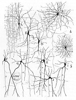
From "Texture of the Nervous System of Man and the Vertebrates" by Santiago Ramón y Cajal. The figure illustrates the diversity of neuronal morphologies in the auditory cortex.
 
Early treatments of neural networks can be found in Herbert Spencer's Principles of Psychology, 3rd edition (1872), Theodor Meynert's Psychiatry (1884), William James' Principles of Psychology (1890), and Sigmund Freud's Project for a Scientific Psychology (composed 1895). The first rule of neuronal learning was described by Hebb in 1949, in the Hebbian theory. Thus, Hebbian pairing of pre-synaptic and post-synaptic activity can substantially alter the dynamic characteristics of the synaptic connection and therefore either facilitate or inhibit signal transmission. In 1959, the neuroscientists, Warren Sturgis McCulloch and Walter Pitts published the first works on the processing of neural networks. They showed theoretically that networks of artificial neurons could implement logical, arithmetic, and symbolic functions. Simplified models of biological neurons were set up, now usually called perceptrons or artificial neurons. These simple models accounted for neural summation (i.e., potentials at the post-synaptic membrane will summate in the cell body). Later models also provided for excitatory and inhibitory synaptic transmission.

Connections between neurons

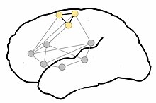
Proposed organization of motor-semantic neural circuits for action language comprehension. Gray dots represent areas of language comprehension, creating a network for comprehending all language. The semantic circuit of the motor system, particularly the motor representation of the legs (yellow dots), is incorporated when leg-related words are comprehended. Adapted from Shebani et al. (2013)
 
The connections between neurons in the brain are much more complex than those of the artificial neurons used in the connectionist neural computing models of artificial neural networks. The basic kinds of connections between neurons are synapses, chemical and electrical synapses

The establishment of synapses enables the connection of neurons into millions of overlapping, and interlinking neural circuits. Neurexins are central to this process.

One principle by which neurons work is neural summationpotentials at the postsynaptic membrane will sum up in the cell body. If the depolarization of the neuron at the axon goes above threshold an action potential will occur that travels down the axon to the terminal endings to transmit a signal to other neurons. Excitatory and inhibitory synaptic transmission is realized mostly by inhibitory postsynaptic potentials (IPSPs) and excitatory postsynaptic potentials (EPSPs). 

On the electrophysiological level, there are various phenomena which alter the response characteristics of individual synapses (called synaptic plasticity) and individual neurons (intrinsic plasticity). These are often divided into short-term plasticity and long-term plasticity. Long-term synaptic plasticity is often contended to be the most likely memory substrate. Usually the term "neuroplasticity" refers to changes in the brain that are caused by activity or experience.

Connections display temporal and spatial characteristics. Temporal characteristics refer to the continuously modified activity-dependent efficacy of synaptic transmission, called spike-timing-dependent plasticity. It has been observed in several studies that the synaptic efficacy of this transmission can undergo short-term increase (called facilitation) or decrease (depression) according to the activity of the presynaptic neuron. The induction of long-term changes in synaptic efficacy, by long-term potentiation (LTP) or depression (LTD), depends strongly on the relative timing of the onset of the excitatory postsynaptic potential and the postsynaptic action potential. LTP is induced by a series of action potentials which cause a variety of biochemical responses. Eventually, the reactions cause the expression of new receptors on the cellular membranes of the postsynaptic neurons or increase the efficacy of the existing receptors through phosphorylation.

Backpropagating action potentials cannot occur because after an action potential travels down a given segment of the axon, the m gates on voltage-gated sodium channels close, thus blocking any transient opening of the h gate from causing a change in the intracellular sodium ion (Na+) concentration, and preventing the generation of an action potential back towards the cell body. In some cells, however, neural backpropagation does occur through the dendritic branching and may have important effects on synaptic plasticity and computation. 

A neuron in the brain requires a single signal to a neuromuscular junction to stimulate contraction of the postsynaptic muscle cell. In the spinal cord, however, at least 75 afferent neurons are required to produce firing. This picture is further complicated by variation in time constant between neurons, as some cells can experience their EPSPs over a wider period of time than others. 

While in synapses in the developing brain synaptic depression has been particularly widely observed it has been speculated that it changes to facilitation in adult brains.

Circuitry

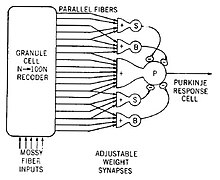
Model of a neural circuit in the cerebellum
 
An example of a neural circuit is the trisynaptic circuit in the hippocampus. Another is the Papez circuit linking the hypothalamus to the limbic lobe. There are several neural circuits in the cortico-basal ganglia-thalamo-cortical loop. These circuits carry information between the cortex, basal ganglia, thalamus, and back to the cortex. The largest structure within the basal ganglia, the striatum, is seen as having its own internal microcircuitry.

Neural circuits in the spinal cord called central pattern generators are responsible for controlling motor instructions involved in rhythmic behaviours. Rhythmic behaviours include walking, urination, and ejaculation. The central pattern generators are made up of different groups of spinal interneurons.

There are four principal types of neural circuits that are responsible for a broad scope of neural functions. These circuits are a diverging circuit, a converging circuit, a reverberating circuit, and a parallel after-discharge circuit.

In a diverging circuit, one neuron synapses with a number of postsynaptic cells. Each of these may synapse with many more making it possible for one neuron to stimulate up to thousands of cells. This is exemplified in the way that thousands of muscle fibers can be stimulated from the initial input from a single motor neuron.

In a converging circuit, inputs from many sources are converged into one output, affecting just one neuron or a neuron pool. This type of circuit is exemplified in the respiratory center of the brainstem, which responds to a number of inputs from different sources by giving out an appropriate breathing pattern.

A reverberating circuit produces a repetitive output. In a signalling procedure from one neuron to another in a linear sequence, one of the neurons may send a signal back to initiating neuron. Each time that the first neuron fires, the other neuron further down the sequence fires again sending it back to the source. This restimulates the first neuron and also allows the path of transmission to continue to its output. A resulting repetitive pattern is the outcome that only stops if one or more of the synapses fail, or if an inhibitory feed from another source causes it to stop. This type of reverberating circuit is found in the respiratory center that sends signals to the respiratory muscles, causing inhalation. When the circuit is interrupted by an inhibitory signal the muscles relax causing exhalation. This type of circuit may play a part in epileptic seizures.

In a parallel after-discharge circuit, a neuron inputs to several chains of neurons. Each chain is made up of a different number of neurons but their signals converge onto one output neuron. Each synapse in the circuit acts to delay the signal by about 0.5 msec so that the more synapses there are will produce a longer delay to the output neuron. After the input has stopped, the output will go on firing for some time. This type of circuit does not have a feedback loop as does the reverberating circuit. Continued firing after the stimulus has stopped is called after-discharge. This circuit type is found in the reflex arcs of certain reflexes.

Study methods

Different neuroimaging techniques have been developed to investigate the activity of neural circuits and networks. The use of "brain scanners" or functional neuroimaging to investigate the structure or function of the brain is common, either as simply a way of better assessing brain injury with high resolution pictures, or by examining the relative activations of different brain areas. Such technologies may include functional magnetic resonance imaging (fMRI), brain positron emission tomography (brain PET), and computed axial tomography (CAT) scans. Functional neuroimaging uses specific brain imaging technologies to take scans from the brain, usually when a person is doing a particular task, in an attempt to understand how the activation of particular brain areas is related to the task. In functional neuroimaging, especially fMRI, which measures hemodynamic activity (using BOLD-contrast imaging) which is closely linked to neural activity, PET, and electroencephalography (EEG) is used. 

Connectionist models serve as a test platform for different hypotheses of representation, information processing, and signal transmission. Lesioning studies in such models, e.g. artificial neural networks, where parts of the nodes are deliberately destroyed to see how the network performs, can also yield important insights in the working of several cell assemblies. Similarly, simulations of dysfunctional neurotransmitters in neurological conditions (e.g., dopamine in the basal ganglia of Parkinson's patients) can yield insights into the underlying mechanisms for patterns of cognitive deficits observed in the particular patient group. Predictions from these models can be tested in patients or via pharmacological manipulations, and these studies can in turn be used to inform the models, making the process iterative.

Clinical significance

Sometimes neural circuitries can become pathological and cause problems such as in Parkinson's disease when the basal ganglia are involved. Problems in the Papez circuit can also give rise to a number of neurodegenerative disorders including Parkinson's.

Printed electronics

From Wikipedia, the free encyclopedia

Gravure printing of electronic structures on paper
 
Printed electronics is a set of printing methods used to create electrical devices on various substrates. Printing typically uses common printing equipment suitable for defining patterns on material, such as screen printing, flexography, gravure, offset lithography, and inkjet. By electronic industry standards, these are low cost processes. Electrically functional electronic or optical inks are deposited on the substrate, creating active or passive devices, such as thin film transistors; capacitors; coils; resistors. Printed electronics is expected to facilitate widespread, very low-cost, low-performance electronics for applications such as flexible displays, smart labels, decorative and animated posters, and active clothing that do not require high performance.

The term printed electronics is often related to organic electronics or plastic electronics, in which one or more inks are composed of carbon-based compounds. These other terms refer to the ink material, which can be deposited by solution-based, vacuum-based or other processes. Printed electronics, in contrast, specifies the process, and, subject to the specific requirements of the printing process selected, can utilize any solution-based material. This includes organic semiconductors, inorganic semiconductors, metallic conductors, nanoparticles, and nanotubes

For the preparation of printed electronics nearly all industrial printing methods are employed. Similar to conventional printing, printed electronics applies ink layers one atop another. So the coherent development of printing methods and ink materials are the field's essential tasks. 

The most important benefit of printing is low-cost volume fabrication. The lower cost enables use in more applications. An example is RFID-systems, which enable contactless identification in trade and transport. In some domains, such as light-emitting diodes printing does not impact performance. Printing on flexible substrates allows electronics to be placed on curved surfaces, for example, printing solar cells on vehicle roofs. More typically, conventional semiconductors justify their much higher costs by providing much higher performance. 

Printed and conventional electronics as complementary technologies.

Resolution, registration, thickness, holes, materials

The maximum required resolution of structures in conventional printing is determined by the human eye. Feature sizes smaller than approximately 20 µm cannot be distinguished by the human eye and consequently exceed the capabilities of conventional printing processes. In contrast, higher resolution and smaller structures are necessary in much electronics printing, because they directly affect circuit density and functionality (especially transistors). A similar requirement holds for the precision with which layers are printed on top of each other (layer to layer registration). 

Control of thickness, holes, and material compatibility (wetting, adhesion, solubility) are essential, but matter in conventional printing only if the eye can detect them. Conversely, the visual impression is irrelevant for printed electronics.

Printing technologies

The attraction of printing technology for the fabrication of electronics mainly results from the possibility of preparing stacks of micro-structured layers (and thereby thin-film devices) in a much simpler and cost-effective way compared to conventional electronics. Also, the ability to implement new or improved functionalities (e.g. mechanical flexibility) plays a role. The selection of the printing method used is determined by requirements concerning printed layers, by the properties of printed materials as well as economic and technical considerations of the final printed products. 

Printing technologies divide between sheet-based and roll-to-roll-based approaches. Sheet-based inkjet and screen printing are best for low-volume, high-precision work. Gravure, offset and flexographic printing are more common for high-volume production, such as solar cells, reaching 10.000 square meters per hour (m²/h). While offset and flexographic printing are mainly used for inorganic and organic conductors (the latter also for dielectrics), gravure printing is especially suitable for quality-sensitive layers like organic semiconductors and semiconductor/dielectric-interfaces in transistors, due to high layer quality. If high resolution is needed, gravure is also suitable for inorganic and organic conductors. Organic field-effect transistors and integrated circuits can be prepared completely by means of mass-printing methods.

Inkjet printing

Inkjets are flexible and versatile, and can be set up with relatively low effort. However, inkjets offer lower throughput of around 100 m2/h and lower resolution (ca. 50 µm). It is well suited for low-viscosity, soluble materials like organic semiconductors. With high-viscosity materials, like organic dielectrics, and dispersed particles, like inorganic metal inks, difficulties due to nozzle clogging occur. Because ink is deposited via droplets, thickness and dispersion homogeneity is reduced. Using many nozzles simultaneously and pre-structuring the substrate allows improvements in productivity and resolution, respectively. However, in the latter case non-printing methods must be employed for the actual patterning step. Inkjet printing is preferable for organic semiconductors in organic field-effect transistors (OFETs) and organic light-emitting diodes (OLEDs), but also OFETs completely prepared by this method have been demonstrated. Frontplanes and backplanes of OLED-displays, integrated circuits, organic photovoltaic cells (OPVCs) and other devices can be prepared with inkjets.

Screen printing

Screen printing is appropriate for fabricating electrics and electronics due to its ability to produce patterned, thick layers from paste-like materials. This method can produce conducting lines from inorganic materials (e.g. for circuit boards and antennas), but also insulating and passivating layers, whereby layer thickness is more important than high resolution. Its 50 m²/h throughput and 100 µm resolution are similar to inkjets. This versatile and comparatively simple method is used mainly for conductive and dielectric layers, but also organic semiconductors, e.g. for OPVCs, and even complete OFETs can be printed.

Aerosol jet printing

Aerosol Jet Printing (also known as Maskless Mesoscale Materials Deposition or M3D) is another material deposition technology for printed electronics. The Aerosol Jet process begins with atomization of an ink, via ultrasonic or pneumatic means, producing droplets on the order of one to two micrometres in diameter. The droplets then flow through a virtual impactor which deflects the droplets having lower momentum away from the stream. This step helps maintaining a tight droplet size distribution. The droplets are entrained in a gas stream and delivered to the print head. Here, an annular flow of clean gas is introduced around the aerosol stream to focus the droplets into a tightly collimated beam of material. The combined gas streams exit the print head through a converging nozzle that compresses the aerosol stream to a diameter as small as 10 µm. The jet of droplets exits the print head at high velocity (~50 meters/second) and impinges upon the substrate. 

Electrical interconnects, passive and active components are formed by moving the print head, equipped with a mechanical stop/start shutter, relative to the substrate. The resulting patterns can have features ranging from 10 µm wide, with layer thicknesses from tens of nanometers to >10 µm. A wide nozzle print head enables efficient patterning of millimeter size electronic features and surface coating applications. All printing occurs without the use of vacuum or pressure chambers. The high exit velocity of the jet enables a relatively large separation between the print head and the substrate, typically 2–5 mm. The droplets remain tightly focused over this distance, resulting in the ability to print conformal patterns over three dimensional substrates. 

Despite the high velocity, the printing process is gentle; substrate damage does not occur and there is generally minimal splatter or overspray from the droplets. Once patterning is complete, the printed ink typically requires post treatment to attain final electrical and mechanical properties. Post-treatment is driven more by the specific ink and substrate combination than by the printing process. A wide range of materials has been successfully deposited with the Aerosol Jet process, including diluted thick film pastes, nanoparticle inks, thermosetting polymers such as UV-curable epoxies, and solvent-based polymers like polyurethane and polyimide, and biologic materials.

Evaporation printing

Evaporation printing uses a combination of high precision screen printing with material vaporization to print features to 5 µm. This method uses techniques such as thermal, e-beam, sputter and other traditional production technologies to deposit materials through a high precision shadow mask (or stencil) that is registered to the substrate to better than 1 micrometer. By layering different mask designs and/or adjusting materials, reliable, cost-effective circuits can be built additively, without the use of photolithography.

Other methods

Other methods with similarities to printing, among them microcontact printing and nano-imprint lithography are of interest. Here, µm- and nm-sized layers, respectively, are prepared by methods similar to stamping with soft and hard forms, respectively. Often the actual structures are prepared subtractively, e.g. by deposition of etch masks or by lift-off processes. For example, electrodes for OFETs can be prepared. Sporadically pad printing is used in a similar manner. Occasionally so-called transfer methods, where solid layers are transferred from a carrier to the substrate, are considered printed electronics. Electrophotography is currently not used in printed electronics.

Materials

Both organic and inorganic materials are used for printed electronics. Ink materials must be available in liquid form, for solution, dispersion or suspension. They must function as conductors, semiconductors, dielectrics, or insulators. Material costs must be fit for the application. 

Electronic functionality and printability can interfere with each other, mandating careful optimization. For example, a higher molecular weight in polymers enhances conductivity, but diminishes solubility. For printing, viscosity, surface tension and solid content must be tightly controlled. Cross-layer interactions such as wetting, adhesion, and solubility as well as post-deposition drying procedures affect the outcome. Additives often used in conventional printing inks are unavailable, because they often defeat electronic functionality. 

Material properties largely determine the differences between printed and conventional electronics. Printable materials provide decisive advantages beside printability, such as mechanical flexibility and functional adjustment by chemical modification (e.g. light color in OLEDs).

Printed conductors offer lower conductivity and charge carrier mobility.

With a few exceptions, inorganic ink materials are dispersions of metallic or semiconducting micro- and nano-particles. Semiconducting nanoparticles used include silicon and oxide semiconductors. Silicon is also printed as an organic precursor which is then converted by pyrolisis and annealing into crystalline silicon. 

PMOS but not CMOS is possible in printed electronics.

Organic materials

Organic printed electronics integrates knowledge and developments from printing, electronics, chemistry, and materials science, especially from organic and polymer chemistry. Organic materials in part differ from conventional electronics in terms of structure, operation and functionality, which influences device and circuit design and optimization as well as fabrication method.

The discovery of conjugated polymers and their development into soluble materials provided the first organic ink materials. Materials from this class of polymers variously possess conducting, semiconducting, electroluminescent, photovoltaic and other properties. Other polymers are used mostly as insulators and dielectrics.

In most organic materials, hole transport is favored over electron transport. Recent studies indicate that this is a specific feature of organic semiconductor/dielectric-interfaces, which play a major role in OFETs. Therefore, p-type devices should dominate over n-type devices. Durability (resistance to dispersion) and lifetime is less than conventional materials.

Organic semiconductors include the conductive polymers poly(3,4-ethylene dioxitiophene), doped with poly(styrene sulfonate), (PEDOT:PSS) and poly(aniline) (PANI). Both polymers are commercially available in different formulations and have been printed using inkjet, screen and offset printing or screen, flexo and gravure printing, respectively.

Polymer semiconductors are processed using inkjet printing, such as poly(thiopene)s like poly(3-hexylthiophene) (P3HT) and poly(9,9-dioctylfluorene co-bithiophen) (F8T2). The latter material has also been gravure printed. Different electroluminescent polymers are used with inkjet printing, as well as active materials for photovoltaics (e.g. blends of P3HT with fullerene derivatives), which in part also can be deposited using screen printing (e.g. blends of poly(phenylene vinylene) with fullerene derivatives).

Printable organic and inorganic insulators and dielectrics exist, which can be processed with different printing methods.

Inorganic materials

Inorganic electronics provides highly ordered layers and interfaces that organic and polymer materials cannot provide.

Silver nanoparticles are used with flexo, offset and inkjet. Gold particles are used with inkjet.

A.C. electroluminescent (EL) multi-color displays can cover many tens of square meters, or be incorporated in watch faces and instrument displays. They involve six to eight printed inorganic layers, including a copper doped phosphor, on a plastic film substrate.

CIGS cells can be printed directly onto molybdenum coated glass sheets.

A printed gallium arsenide germanium solar cell demonstrated 40.7% conversion efficiency, eight times that of the best organic cells, approaching the best performance of crystalline silicon.

Substrates

Printed electronics allows the use of flexible substrates, which lowers production costs and allows fabrication of mechanically flexible circuits. While inkjet and screen printing typically imprint rigid substrates like glass and silicon, mass-printing methods nearly exclusively use flexible foil and paper. Poly(ethylene terephthalate)-foil (PET) is a common choice, due to its low cost and moderately high temperature stability. Poly(ethylene naphthalate)- (PEN) and poly(imide)-foil (PI) are higher performance, higher cost alternatives. Paper's low costs and manifold applications make it an attractive substrate, however, its high roughness and high wettability have traditionally made it problematic for electronics. This is an active research area, however, and print-compatible metal deposition techniques have been demonstrated that adapt to the rough 3D surface geometry of paper.

Other important substrate criteria are low roughness and suitable wet-ability, which can be tuned pre-treatment by use of coating or Corona discharge. In contrast to conventional printing, high absorbency is usually disadvantageous.

History

Albert Hanson, a German by birth, is credited to have introduced the concept of printed electronics. in 1903 he filled a patent for “Printed Wires,” and thus printed electronics were born. Hanson proposed forming a Printed Circuit Board pattern on copper foil through cutting or stamping. The drawn elements were glued to the dielectric, in this case, paraffined paper. The first printed circuit was produced in 1936 by Paul Eisler, and that process was used for large-scale production of radios by the USA during World War II. Printed circuit technology was released for commercial use in the USA in 1948 (Printed Circuits Handbook, 1995). In the over a half-century since its inception, printed electronics has evolved from the production of printed circuit boards (PCBs), through the everyday use of membrane switches, to today’s RFID, photovoltaic and electroluminescent technologies. Today it is nearly impossible to look around a modern American household and not see devices that either uses printed electronic components or that are the direct result of printed electronic technologies. Widespread production of printed electronics for household use began in the 1960s when the Printed Circuit Board became the foundation for all consumer electronics. Since then printed electronics have become a cornerstone in many new commercial products.

The biggest trend in recent history when it comes to printed electronics is the widespread use of them in solar cells. In 2011, researchers from MIT created a flexible solar cell by inkjet printing on normal paper. In 2018, researchers at Rice University have developed organic solar cells which can be painted or printed onto surfaces. These solar cells have been shown to max out at fifteen percent efficiency. Konarka Technologies, now a defunct company in the USA, was the pioneering company in producing inkjet solar cells. Today there are more than fifty companies across a diverse number of countries that are producing printed solar cells.

While printed electronics have been around since the 1960s, they are predicted to have a major boom in total revenue. As of 2011, the total printed electronic revenue was reported to be at $12,385 (million). A report by IDTechEx predicts the PE market will reach $330 (billion) in 2027. A big reason for this increase in revenue is because of the incorporation of printed electronic into cellphones. Nokia was on of the companies that pioneered the idea of creating a “Morph” phone using printed electronics. Since then, Apple has implemented this technology into their iPhone XS, XS Max, and XR devices. Printed electronics can be used to make all of the following components of a cellphone: 3D main antenna, GPS antenna, energy storage, 3D interconnections, multi-layer PCB, edge circuits, ITO jumpers, hermetic seals, LED packaging, and tactile feedback. 

With the revolutionary discoveries and advantages that printed electronic gives to companies many large companies have made recent investments into this technology. In 2007, Soligie Inc. and Thinfilm Electronics entered into an agreement to combine IPs for soluble memory materials and functional materials printing to develop printed memory in commercial volumes. LG announce significant investment, potentially $8.71 billion in OLEDs on Plastic. Sharp (Foxconn) will invest $570m in pilot line for OLED displays. BOE announce potential $6.8 billion in flexible AMOLED fab. Heliatek has secured €80m in additional funding for OPV manufacturing in Dresden. PragmatIC has raised ~ €20m from investors including Avery Dennison. Thinfilm invests in new production site in Silicon Valley (formerly owned by Qualcomm). Cambrios back in business after acquisition by TPK.

Applications

Printed electronics are in use or under consideration for:
Norwegian company ThinFilm demonstrated roll-to-roll printed organic memory in 2009.

Standards development and activities

Technical standards and roadmapping initiatives are intended to facilitate value chain development (for sharing of product specifications, characterization standards, etc.) This strategy of standards development mirrors the approach used by silicon-based electronics over the past 50 years. Initiatives include:
IPC—Association Connecting Electronics Industries has published three standards for printed electronics. All three have been published in cooperation with the Japan Electronic Packaging and Circuits Association (JPCA):
  • IPC/JPCA-4921, Requirements for Printed Electronics Base Materials
  • IPC/JPCA-4591, Requirements for Printed Electronics Functional Conductive Materials
  • IPC/JPCA-2291, Design Guideline for Printed Electronics
These standards, and others in development, are part of IPC’s Printed Electronics Initiative.

Boron nitride

From Wikipedia, the free encyclopedia

Boron nitride
Magnified sample of crystalline hexagonal boron nitride
Names
IUPAC name
Boron nitride
Identifiers
3D model (JSmol)
ChEBI
ChemSpider
ECHA InfoCard 100.030.111
EC Number 233-136-6
216
MeSH Elbor
PubChem CID
RTECS number ED7800000
UNII
Properties
BN
Molar mass 24.82 g·mol−1
Appearance Colorless crystals
Density 2.1 (h-BN); 3.45 (c-BN) g/cm3
Melting point 2,973 °C (5,383 °F; 3,246 K) sublimates (cBN)
insoluble
Electron mobility 200 cm2/(V·s) (cBN)
1.8 (h-BN); 2.1 (c-BN)
Structure
hexagonal, sphalerite, wurtzite
Thermochemistry
19.7 J/(K·mol)
14.8 J/K mol
-254.4 kJ/mol
-228.4 kJ/mol
Hazards
Irritant Xi
R-phrases (outdated) R36/37
S-phrases (outdated) S26, S36
NFPA 704
Flammability code 0: Will not burn. E.g., waterHealth code 0: Exposure under fire conditions would offer no hazard beyond that of ordinary combustible material. E.g., sodium chlorideReactivity code 0: Normally stable, even under fire exposure conditions, and is not reactive with water. E.g., liquid nitrogenSpecial hazards (white): no codeNFPA 704 four-colored diamond
0
0
0
Related compounds
Related compounds
Boron arsenide Boron carbide Boron phosphide Boron trioxide
Except where otherwise noted, data are given for materials in their standard state (at 25 °C [77 °F], 100 kPa).

Boron nitride is a heat and chemically resistant refractory compound of boron and nitrogen with the chemical formula BN. It exists in various crystalline forms that are isoelectronic to a similarly structured carbon lattice. The hexagonal form corresponding to graphite is the most stable and soft among BN polymorphs, and is therefore used as a lubricant and an additive to cosmetic products. The cubic (sphalerite structure) variety analogous to diamond is called c-BN; it is softer than diamond, but its thermal and chemical stability is superior. The rare wurtzite BN modification is similar to lonsdaleite and may even be harder than the cubic form.

Because of excellent thermal and chemical stability, boron nitride ceramics are traditionally used as parts of high-temperature equipment. Boron nitride has potential use in nanotechnology. Nanotubes of BN can be produced that have a structure similar to that of carbon nanotubes, i.e. graphene (or BN) sheets rolled on themselves, but the properties are very different.

Structure

Boron nitride exists in multiple forms that differ in the arrangement of the boron and nitrogen atoms, giving rise to varying bulk properties of the material.

Amorphous form (a-BN)

The amorphous form of boron nitride (a-BN) is non-crystalline, lacking any long-distance regularity in the arrangement of its atoms. It is analogous to amorphous carbon.

All other forms of boron nitride are crystalline.

Hexagonal form (h-BN)

The most stable crystalline form is the hexagonal one, also called h-BN, α-BN, g-BN, and graphitic boron nitride. Hexagonal boron nitride (point group = D6h; space group = P63/mmc) has a layered structure similar to graphite. Within each layer, boron and nitrogen atoms are bound by strong covalent bonds, whereas the layers are held together by weak van der Waals forces. The interlayer "registry" of these sheets differs, however, from the pattern seen for graphite, because the atoms are eclipsed, with boron atoms lying over and above nitrogen atoms. This registry reflects the polarity of the B–N bonds. Still, h-BN and graphite are very close neighbors and even the BC6N hybrids have been synthesized where carbon substitutes for some B and N atoms.

Cubic form (c-BN)

Cubic boron nitride has a crystal structure analogous to that of diamond. Consistent with diamond being less stable than graphite, the cubic form is less stable than the hexagonal form, but the conversion rate between the two is negligible at room temperature, as it is for diamond. The cubic form has the sphalerite crystal structure, the same as that of diamond, and is also called β-BN or c-BN.

Wurtzite form (w-BN)

The wurtzite form of boron nitride (w-BN; point group = C6v; space group = P63mc) has the same structure as lonsdaleite, a rare hexagonal polymorph of carbon. As in the cubic form, the boron and nitrogen atoms are grouped into tetrahedra, but in w-BN the angles between neighboring tetrahedra are different. As in the cubic form, the boron and nitrogen atoms are grouped into 6-membered rings; in the cubic form all rings are in the chair configuration, in w-BN the rings between 'layers' are in boat configuration. The Wurtzite form is thought to be very strong, and was estimated by a simulation as potentially having a strength 18% stronger than that of diamond, but because only small amounts of the mineral exist in nature, this has not yet been experimentally verified.

Properties

Physical

Properties of amorphous and crystalline BN, graphite and diamond.
Some properties of h-BN and graphite differ within the basal planes (∥) and perpendicular to them (⟂)
Material a-BN h-BN c-BN w-BN graphite diamond
Density (g/cm3) 2.28 ~2.1 3.45 3.49 ~2.1 3.515
Knoop hardness (GPa) 10
45 34
100
Bulk modulus (GPa) 100 36.5 400 400 34 440
Thermal conductivity (W/(m·K)) 3 600 ∥, 30 ⟂ 740
200–2000 ∥, 2–800 ⟂ 600–2000
Thermal expansion (10−6/°C)
−2.7 ∥, 38 ⟂ 1.2 2.7 −1.5 ∥, 25 ⟂ 0.8
Bandgap (eV) 5.05 5.2 6.4 4.5–5.5 0 5.5
Refractive index 1.7 1.8 2.1 2.05
2.4
Magnetic susceptibility (µemu/g)
−0.48 ∥, −17.3 ⟂

−0.2...−2.7 ∥, −20...−28 ⟂ −1.6

The partly ionic structure of BN layers in h-BN reduces covalency and electrical conductivity, whereas the interlayer interaction increases resulting in higher hardness of h-BN relative to graphite. The reduced electron-delocalization in hexagonal-BN is also indicated by its absence of color and a large band gap. Very different bonding – strong covalent within the basal planes (planes where boron and nitrogen atoms are covalently bonded) and weak between them – causes high anisotropy of most properties of h-BN. 

For example, the hardness, electrical and thermal conductivity are much higher within the planes than perpendicular to them. On the contrary, the properties of c-BN and w-BN are more homogeneous and isotropic.
Those materials are extremely hard, with the hardness of bulk c-BN being slightly smaller and w-BN even higher than that of diamond. Polycrystalline c-BN with grain sizes on the order of 10 nm is also reported to have Vickers hardness comparable or higher than diamond. Because of much better stability to heat and transition metals, c-BN surpasses diamond in mechanical applications, such as machining steel. The thermal conductivity of BN is among the highest of all electric insulators.

Boron nitride can be doped p-type with beryllium and n-type with boron, sulfur, silicon or if co-doped with carbon and nitrogen. Both hexagonal and cubic BN are wide-gap semiconductors with a band-gap energy corresponding to the UV region. If voltage is applied to h-BN or c-BN, then it emits UV light in the range 215–250 nm and therefore can potentially be used as light-emitting diodes (LEDs) or lasers. 

Little is known on melting behavior of boron nitride. It sublimates at 2973 °C at normal pressure releasing nitrogen gas and boron, but melts at elevated pressure.

Thermal stability

Hexagonal and cubic (and probably w-BN) BN show remarkable chemical and thermal stabilities. For example, h-BN is stable to decomposition at temperatures up to 1000 °C in air, 1400 °C in vacuum, and 2800 °C in an inert atmosphere. The reactivity of h-BN and c-BN is relatively similar, and the data for c-BN are summarized in the table below. 

Reactivity of c-BN with solids
Solid Ambient Action Threshold T (°C)
Mo 10−2 Pa vacuum reaction 1360
Ni 10−2 Pa vacuum wetting 1360
Fe, Ni, Co argon react 1400–1500
Al 10−2 Pa vacuum wetting and reaction 1050
Si 10−3 Pa vacuum wetting 1500
Cu, Ag, Au, Ga, In, Ge, Sn 10−3 Pa vacuum no wetting 1100
B
no wetting 2200
Al2O3 + B2O3 10−2 Pa vacuum no reaction 1360

Thermal stability of c-BN can be summarized as follows:
  • In air or oxygen: B2O3 protective layer prevents further oxidation to ~1300 °C; no conversion to hexagonal form at 1400 °C.
  • In nitrogen: some conversion to h-BN at 1525 °C after 12 h.
  • In vacuum (10−5 Pa): conversion to h-BN at 1550–1600 °C.

Chemical stability

Boron nitride is insoluble in the usual acids, but is soluble in alkaline molten salts and nitrides, such as LiOH, KOH, NaOH-Na2CO3, NaNO3, Li3N, Mg3N2, Sr3N2, Ba3N2 or Li3BN2, which are therefore used to etch BN.

Thermal conductivity

The theoretical thermal conductivity of hexagonal Boron nitride nanoribbons (BNNRs) can approach 1700–2000 W/(m·K), which has the same order of magnitude as the experimental measured value for graphene, and can be comparable to the theoretical calculations for graphene nanoribbons. Moreover, the thermal transport in the BNNRs is anisotropic. The thermal conductivity of zigzag-edged BNNRs is about 20% larger than that of armchair-edged nanoribbons at room temperature.

Natural occurrence

In 2009, a naturally occurring boron nitride mineral in the cubic form (c-BN) was reported in Tibet, with a proposed name of qingsongite. The substance was found in dispersed micron-sized inclusions in chromium-rich rocks. In 2013, the International Mineralogical Association affirmed the mineral and the name.

Synthesis

Preparation and reactivity of hexagonal BN

Boron nitride is produced synthetically. Hexagonal boron nitride is obtained by the reacting boron trioxide (B2O3) or boric acid (H3BO3) with ammonia (NH3) or urea (CO(NH2)2) in a nitrogen atmosphere:
B2O3 + 2 NH3 → 2 BN + 3 H2O (T = 900 °C)
B(OH)3 + NH3 → BN + 3 H2O (T = 900 °C)
B2O3 + CO(NH2)2 → 2 BN + CO2 + 2 H2O (T > 1000 °C)
B2O3 + 3 CaB6 + 10 N2 → 20 BN + 3 CaO (T > 1500 °C)
The resulting disordered (amorphous) boron nitride contains 92–95% BN and 5–8% B2O3. The remaining B2O3 can be evaporated in a second step at temperatures > 1500 °C in order to achieve BN concentration >98%. Such annealing also crystallizes BN, the size of the crystallites increasing with the annealing temperature.

h-BN parts can be fabricated inexpensively by hot-pressing with subsequent machining. The parts are made from boron nitride powders adding boron oxide for better compressibility. Thin films of boron nitride can be obtained by chemical vapor deposition from boron trichloride and nitrogen precursors. Combustion of boron powder in nitrogen plasma at 5500 °C yields ultrafine boron nitride used for lubricants and toners.

Boron nitride reacts with iodine fluoride in trichlorofluoromethane at −30 °C to produce an extremely sensitive contact explosive, NI3, in low yield. Boron nitride reacts with nitrides of alkali metals and lanthanides to form nitridoborate compounds. For example:
Li3N + BN → Li3BN2

Intercalation of hexagonal BN

Structure of hexagonal boron nitride intercalated with potassium (B4N4K)
 
Similar to graphite, various molecules, such as NH3 or alkali metals, can be intercalated into hexagonal boron nitride, that is inserted between its layers. Both experiment and theory suggest the intercalation is much more difficult for BN than for graphite.

Preparation of cubic BN

Synthesis of c-BN uses same methods as that of diamond: Cubic boron nitride is produced by treating hexagonal boron nitride at high pressure and temperature, much as synthetic diamond is produced from graphite. Direct conversion of hexagonal boron nitride to the cubic form has been observed at pressures between 5 and 18 GPa and temperatures between 1730 and 3230 °C, that is similar parameters as for direct graphite-diamond conversion. The addition of a small amount of boron oxide can lower the required pressure to 4–7 GPa and temperature to 1500 °C. As in diamond synthesis, to further reduce the conversion pressures and temperatures, a catalyst is added, such as lithium, potassium, or magnesium, their nitrides, their fluoronitrides, water with ammonium compounds, or hydrazine. Other industrial synthesis methods, again borrowed from diamond growth, use crystal growth in a temperature gradient, or explosive shock wave. The shock wave method is used to produce material called heterodiamond, a superhard compound of boron, carbon, and nitrogen.

Low-pressure deposition of thin films of cubic boron nitride is possible. As in diamond growth, the major problem is to suppress the growth of hexagonal phases (h-BN or graphite, respectively). Whereas in diamond growth this is achieved by adding hydrogen gas, boron trifluoride is used for c-BN. Ion beam deposition, plasma-enhanced chemical vapor deposition, pulsed laser deposition, reactive sputtering, and other physical vapor deposition methods are used as well.

Preparation of wurtzite BN

Wurtzite BN can be obtained via static high-pressure or dynamic shock methods. The limits of its stability are not well defined. Both c-BN and w-BN are formed by compressing h-BN, but formation of w-BN occurs at much lower temperatures close to 1700 °C.

Production statistics

Whereas the production and consumption figures for the raw materials used for BN synthesis, namely boric acid and boron trioxide, are well known, the corresponding numbers for the boron nitride are not listed in statistical reports. An estimate for the 1999 world production is 300 to 350 metric tons. The major producers and consumers of BN are located in the United States, Japan, China and Germany. In 2000, prices varied from about $75/kg to $120/kg for standard industrial-quality h-BN and were about up to $200–$400/kg for high purity BN grades.

Applications

Hexagonal BN

Ceramic BN crucible
 
Hexagonal BN (h-BN) is the most widely used polymorph. It is a good lubricant at both low and high temperatures (up to 900 °C, even in an oxidizing atmosphere). h-BN lubricant is particularly useful when the electrical conductivity or chemical reactivity of graphite (alternative lubricant) would be problematic. Another advantage of h-BN over graphite is that its lubricity does not require water or gas molecules trapped between the layers. Therefore, h-BN lubricants can be used even in vacuum, e.g. in space applications. The lubricating properties of fine-grained h-BN are used in cosmetics, paints, dental cements, and pencil leads.

Hexagonal BN was first used in cosmetics around 1940 in Japan. However, because of its high price, h-BN was soon abandoned for this application. Its use was revitalized in the late 1990s with the optimization h-BN production processes, and currently h-BN is used by nearly all leading producers of cosmetic products for foundations, make-up, eye shadows, blushers, kohl pencils, lipsticks and other skincare products.

Because of its excellent thermal and chemical stability, boron nitride ceramics are traditionally used as parts of high-temperature equipment. h-BN can be included in ceramics, alloys, resins, plastics, rubbers, and other materials, giving them self-lubricating properties. Such materials are suitable for construction of e.g. bearings and in steelmaking. Plastics filled with BN have less thermal expansion as well as higher thermal conductivity and electrical resistivity. Due to its excellent dielectric and thermal properties, BN is used in electronics e.g. as a substrate for semiconductors, microwave-transparent windows and as a structural material for seals. It can also be used as dielectric in resistive random access memories.

Hexagonal BN is used in xerographic process and laser printers as a charge leakage barrier layer of the photo drum. In the automotive industry, h-BN mixed with a binder (boron oxide) is used for sealing oxygen sensors, which provide feedback for adjusting fuel flow. The binder utilizes the unique temperature stability and insulating properties of h-BN.

Parts can be made by hot pressing from four commercial grades of h-BN. Grade HBN contains a boron oxide binder; it is usable up to 550–850 °C in oxidizing atmosphere and up to 1600 °C in vacuum, but due to the boron oxide content is sensitive to water. Grade HBR uses a calcium borate binder and is usable at 1600 °C. Grades HBC and HBT contain no binder and can be used up to 3000 °C.

Boron nitride nanosheets (h-BN) can be deposited by catalytic decomposition of borazine at a temperature ~1100 °C in a chemical vapor deposition setup, over areas up to about 10 cm2. Owing to their hexagonal atomic structure, small lattice mismatch with graphene (~2%), and high uniformity they are used as substrates for graphene-based devices. BN nanosheets are also excellent proton conductors. Their high proton transport rate, combined with the high electrical resistance, may lead to applications in fuel cells and water electrolysis.

h-BN has been used since the mid-2000s as a bullet and bore lubricant in precision target rifle applications as an alternative to molybdenum disulfide coating, commonly referred to as "moly". It is claimed to increase effective barrel life, increase intervals between bore cleaning, and decrease the deviation in point of impact between clean bore first shots and subsequent shots.

Cubic boron nitride

Cubic boron nitride (CBN or c-BN) is widely used as an abrasive. Its usefulness arises from its insolubility in iron, nickel, and related alloys at high temperatures, whereas diamond is soluble in these metals. Polycrystalline c-BN (PCBN) abrasives are therefore used for machining steel, whereas diamond abrasives are preferred for aluminum alloys, ceramics, and stone. When in contact with oxygen at high temperatures, BN forms a passivation layer of boron oxide. Boron nitride binds well with metals, due to formation of interlayers of metal borides or nitrides. Materials with cubic boron nitride crystals are often used in the tool bits of cutting tools. For grinding applications, softer binders, e.g. resin, porous ceramics, and soft metals, are used. Ceramic binders can be used as well. Commercial products are known under names "Borazon" (by Diamond Innovations), and "Elbor" or "Cubonite" (by Russian vendors).

Contrary to diamond, large c-BN pellets can be produced in a simple process (called sintering) of annealing c-BN powders in nitrogen flow at temperatures slightly below the BN decomposition temperature. This ability of c-BN and h-BN powders to fuse allows cheap production of large BN parts.

Similar to diamond, the combination in c-BN of highest thermal conductivity and electrical resistivity is ideal for heat spreaders

As cubic boron nitride consists of light atoms and is very robust chemically and mechanically, it is one of the popular materials for X-ray membranes: low mass results in small X-ray absorption, and good mechanical properties allow usage of thin membranes, thus further reducing the absorption.

Amorphous boron nitride

Layers of amorphous boron nitride (a-BN) are used in some semiconductor devices, e.g. MOSFETs. They can be prepared by chemical decomposition of trichloroborazine with caesium, or by thermal chemical vapor deposition methods. Thermal CVD can be also used for deposition of h-BN layers, or at high temperatures, c-BN.

Other forms of boron nitride

Atomically thin boron nitride

Hexagonal boron nitride can be exfoliated to mono or few atomic layer sheets. Due to its analogous structure to that of graphene but white appearance, atomically thin boron nitride is sometimes call “white graphene”.

Mechanical properties. Atomically thin boron nitride is one of the strongest electrically insulating materials. Monolayer boron nitride has an average Young's modulus of 0.865TPa and fracture strength of 70.5GPa, and in contrast to graphene, whose strength decreases dramatically with increased thickness, few-layer boron nitride sheets have a strength similar to that of monolayer boron nitride.

Thermal conductivity. Atomically thin boron nitride has one of the highest thermal conductivity coefficients among semiconductors and electrical insulators, and its thermal conductivity increases with reduced thickness due to less intra-layer coupling.

Thermal stability. The air stability of graphene shows a clear thickness dependence: monolayer graphene is reactive to oxygen at 250 °C, strongly doped at 300 °C, and etched at 450 °C; in contrast, bulk graphite is not oxidized until 800 °C. Atomically thin boron nitride has much better oxidation resistance than graphene. Monolayer boron nitride is not oxidized till 700 °C and can sustain up to 850 °C in air; bilayer and trilayer boron nitride nanosheets have slightly higher oxidation starting temperatures. The excellent thermal stability, high impermeability to gas and liquid, and electrical insulation make atomically thin boron nitride potential coating materials for preventing surface oxidation and corrosion of metals and other two-dimensional (2D) materials, such as black phosphorus.

Better surface adsorption. Atomically thin boron nitride has been found to have better surface adsorption capabilities than bulk hexagonal boron nitride. According to theoretical and experimental studies, atomically thin boron nitride as an adsorbent experiences conformational changes upon surface adsorption of molecules, increasing adsorption energy and efficiency. The synergic effect of the atomic thickness, high flexibility, stronger surface adsorption capability, electrical insulation, impermeability, high thermal and chemical stability of BN nanosheets can increase the Raman sensitivity by up to two orders, and in the meantime attain long-term stability and extraordinary reusability not achievable by other materials.

Dielectric properties. Atomically thin hexagonal boron nitride is an excellent dielectric substrate for graphene, molybdenum disulphide (MoS2), and many other 2D material-based electronic and photonic devices. As shown by electric force microscopy (EFM) studies, the electric field screening in atomically thin boron nitride shows a weak dependence on thickness, which is in line with the smooth decay of electric field inside few-layer boron nitride revealed by the first-principles calculations.

Raman characteristics. Raman spectroscopy has been a useful tool to study a variety of 2D materials, and the Raman signature of high-quality atomically thin boron nitride was first reported by Gorbachev et al. and Li et al. However, the two reported Raman results of monolayer boron nitride did not agree with each other. Cai et al., therefore, conducted systematic experimental and theoretical studies to reveal the intrinsic Raman spectrum of atomically thin boron nitride. It reveals that atomically thin boron nitride without interaction with a substrate has a G band frequency similar to that of bulk hexagonal boron nitride, but strain induced by the substrate can cause Raman shifts. Nevertheless, the Raman intensity of G band of atomically thin boron nitride can be used to estimate layer thickness and sample quality.

BN nanomesh observed with a scanning tunneling microscope. The center of each ring corresponds to the center of the pores
 
Top: absorption of cyclohexane by BN aerogel. Cyclohexane is stained with Sudan II red dye and is floating on water. Bottom: reuse of the aerogel after burning in air.

Boron nitride nanomesh

Boron nitride nanomesh is a nanostructured two-dimensional material. It consists of a single BN layer, which forms by self-assembly a highly regular mesh after high-temperature exposure of a clean rhodium or ruthenium surface to borazine under ultra-high vacuum. The nanomesh looks like an assembly of hexagonal pores. The distance between two pore centers is 3.2 nm and the pore diameter is ~2 nm. Other terms for this material are boronitrene or white graphene.

The boron nitride nanomesh is not only stable to decomposition under vacuum, air and some liquids, but also up to temperatures of 800 °C. In addition, it shows the extraordinary ability to trap molecules and metallic clusters which have similar sizes to the nanomesh pores, forming a well-ordered array. These characteristics promise interesting applications of the nanomesh in areas like catalysis, surface functionalisation, spintronics, quantum computing and data storage media like hard drives.

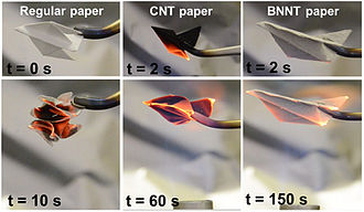
BN nanotubes are flame resistant, as shown in this comparative test of airplanes made of cellullose, carbon buckypaper and BN nanotube buckypaper.

Boron nitride nanotubes

Boron nitride tubules were first made in 1989 by Shore and Dolan This work was patented in 1989 and published in 1989 thesis (Dolan) and then 1993 Science. The 1989 work was also the first preparation of amorphous BN by B-trichloroborazine and cesium metal. 

Preparation of Amorphous Boron Nitride and Its Conversion to a Turbostratic, Tubular Form Ewan J. M. Hamilton1, Shawn E. Dolan1, Charles M. Mann1, Hendrik O. Colijn2, Clare A. McDonald2, Sheldon G. Shore, Science 30 Apr 1993: Vol. 260, Issue 5108, pp. 659–661 DOI: 10.1126/science.260.5108.659 Boron nitride nanotubes were predicted in 1994 and experimentally discovered in 1995. They can be imagined as a rolled up sheet of h-boron nitride. Structurally, it is a close analog of the carbon nanotube, namely a long cylinder with diameter of several to hundred nanometers and length of many micrometers, except carbon atoms are alternately substituted by nitrogen and boron atoms. However, the properties of BN nanotubes are very different: whereas carbon nanotubes can be metallic or semiconducting depending on the rolling direction and radius, a BN nanotube is an electrical insulator with a bandgap of ~5.5 eV, basically independent of tube chirality and morphology. In addition, a layered BN structure is much more thermally and chemically stable than a graphitic carbon structure.

Boron nitride aerogel

Boron nitride aerogel is an aerogel made of highly porous BN. It typically consists of a mixture of deformed BN nanotubes and nanosheets. It can have a density as low as 0.6 mg/cm3 and a specific surface area as high as 1050 m2/g, and therefore has potential applications as an absorbent, catalyst support and gas storage medium. BN aerogels are highly hydrophobic and can absorb up to 160 times their weight in oil. They are resistant to oxidation in air at temperatures up to 1200 °C, and hence can be reused after the absorbed oil is burned out by flame. BN aerogels can be prepared by template-assisted chemical vapor deposition using borazine as the feed gas.

Composites containing BN

Addition of boron nitride to silicon nitride ceramics improves the thermal shock resistance of the resulting material. For the same purpose, BN is added also to silicon nitride-alumina and titanium nitride-alumina ceramics. Other materials being reinforced with BN include alumina and zirconia, borosilicate glasses, glass ceramics, enamels, and composite ceramics with titanium boride-boron nitride, titanium boride-aluminium nitride-boron nitride, and silicon carbide-boron nitride composition.

Health issues

Boron nitride (along with Si3N4, NbN, and BNC) is reported to show weak fibrogenic activity, and to cause pneumoconiosis when inhaled in particulate form. The maximum concentration recommended for nitrides of nonmetals is 10 mg/m3 for BN and 4 for AlN or ZrN.

1947–1948 civil war in Mandatory Palestine

From Wikipedia, the free encyclopedia During the civil war, the Jewish and Arab communities of Palestine clashed (the latter supported b...