Search This Blog

Saturday, September 25, 2021

Solar cell efficiency

From Wikipedia, the free encyclopedia
 
Reported timeline of research solar cell energy conversion efficiencies since 1976 (National Renewable Energy Laboratory)

Solar cell efficiency refers to the portion of energy in the form of sunlight that can be converted via photovoltaics into electricity by the solar cell.

The efficiency of the solar cells used in a photovoltaic system, in combination with latitude and climate, determines the annual energy output of the system. For example, a solar panel with 20% efficiency and an area of 1 m2 will produce 200 kWh/yr at Standard Test Conditions if exposed to the Standard Test Condition solar irradiance value of 1000 W/m2 for 2.74 hours a day. Usually solar panels are exposed to sunlight for longer than this in a given day, but the solar irradiance is less than 1000 W/m2 for most of the day. A solar panel can produce more when the sun is high in the sky and will produce less in cloudy conditions or when the sun is low in the sky. The sun is lower in the sky in the winter. In a high yield solar area like central Colorado, which receives annual insolation of 2000 kWh/m2/year, such a panel can be expected to produce 400 kWh of energy per year. However, in Michigan, which receives only 1400 kWh/m2/year, annual energy yield will drop to 280 kWh for the same panel. At more northerly European latitudes, yields are significantly lower: 175 kWh annual energy yield in southern England under the same conditions.

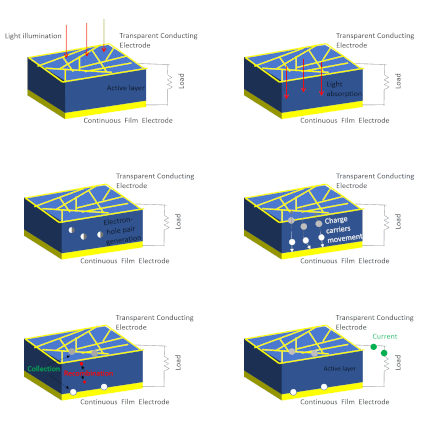
Schematic of charge collection by solar cells. Light transmits through transparent conducting electrode creating electron hole pairs, which are collected by both the electrodes. The absorption and collection efficiencies of a solar cell depend on the design of transparent conductors and active layer thickness.

Several factors affect a cell's conversion efficiency value, including its reflectance, thermodynamic efficiency, charge carrier separation efficiency, charge carrier collection efficiency and conduction efficiency values. Because these parameters can be difficult to measure directly, other parameters are measured instead, including quantum efficiency, open-circuit voltage (VOC) ratio, and § Fill factor (described below). Reflectance losses are accounted for by the quantum efficiency value, as they affect "external quantum efficiency." Recombination losses are accounted for by the quantum efficiency, VOC ratio, and fill factor values. Resistive losses are predominantly accounted for by the fill factor value, but also contribute to the quantum efficiency and VOC ratio values. In 2019, the world record for solar cell efficiency at 47.1% was achieved by using multi-junction concentrator solar cells, developed at National Renewable Energy Laboratory, Golden, Colorado, USA.

Factors affecting energy conversion efficiency

The factors affecting energy conversion efficiency were expounded in a landmark paper by William Shockley and Hans Queisser in 1961.

Thermodynamic efficiency limit and infinite-stack limit

The Shockley–Queisser limit for the efficiency of a single-junction solar cell under unconcentrated sunlight at 273 K. This calculated curve uses actual solar spectrum data, and therefore the curve is wiggly from IR absorption bands in the atmosphere. This efficiency limit of ~34% can be exceeded by multijunction solar cells.

If one has a source of heat at temperature Ts and cooler heat sink at temperature Tc, the maximum theoretically possible value for the ratio of work (or electric power) obtained to heat supplied is 1-Tc/Ts, given by a Carnot heat engine. If we take 6000 K for the temperature of the sun and 300 K for ambient conditions on earth, this comes to 95%. In 1981, Alexis de Vos and Herman Pauwels showed that this is achievable with a stack of an infinite number of cells with band gaps ranging from infinity (the first cells encountered by the incoming photons) to zero, with a voltage in each cell very close to the open-circuit voltage, equal to 95% of the band gap of that cell, and with 6000 K blackbody radiation coming from all directions. However, the 95% efficiency thereby achieved means that the electric power is 95% of the net amount of light absorbed – the stack emits radiation as it has non-zero temperature, and this radiation has to be subtracted from the incoming radiation when calculating the amount of heat being transferred and the efficiency. They also considered the more relevant problem of maximizing the power output for a stack being illuminated from all directions by 6000 K blackbody radiation. In this case, the voltages must be lowered to less than 95% of the band gap (the percentage is not constant over all the cells). The maximum theoretical efficiency calculated is 86.8% for a stack of an infinite number of cells, using the incoming concentrated sunlight radiation. When the incoming radiation comes only from an area of the sky the size of the sun, the efficiency limit drops to 68.7%.

Ultimate efficiency

Normal photovoltaic systems however have only one p–n junction and are therefore subject to a lower efficiency limit, called the "ultimate efficiency" by Shockley and Queisser. Photons with an energy below the band gap of the absorber material cannot generate an electron-hole pair, so their energy is not converted to useful output, and only generates heat if absorbed. For photons with an energy above the band gap energy, only a fraction of the energy above the band gap can be converted to useful output. When a photon of greater energy is absorbed, the excess energy above the band gap is converted to kinetic energy of the carrier combination. The excess kinetic energy is converted to heat through phonon interactions as the kinetic energy of the carriers slows to equilibrium velocity. Traditional single-junction cells with an optimal band gap for the solar spectrum have a maximum theoretical efficiency of 33.16%, the Shockley–Queisser limit .

Solar cells with multiple band gap absorber materials improve efficiency by dividing the solar spectrum into smaller bins where the thermodynamic efficiency limit is higher for each bin.

Quantum efficiency

As described above, when a photon is absorbed by a solar cell it can produce an electron-hole pair. One of the carriers may reach the p–n junction and contribute to the current produced by the solar cell; such a carrier is said to be collected. Or, the carriers recombine with no net contribution to cell current.

Quantum efficiency refers to the percentage of photons that are converted to electric current (i.e., collected carriers) when the cell is operated under short circuit conditions. The "external" quantum efficiency of a silicon solar cell includes the effect of optical losses such as transmission and reflection.

In particular, some measures can be taken to reduce these losses. The reflection losses, which can account for up to 10% of the total incident energy, can be dramatically decreased using a technique called texturization, a light trapping method that modifies the average light path.

Quantum efficiency is most usefully expressed as a spectral measurement (that is, as a function of photon wavelength or energy). Since some wavelengths are absorbed more effectively than others, spectral measurements of quantum efficiency can yield valuable information about the quality of the semiconductor bulk and surfaces. Quantum efficiency alone is not the same as overall energy conversion efficiency, as it does not convey information about the fraction of power that is converted by the solar cell.

Maximum power point

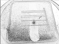
Dust often accumulates on the glass of solar modules - highlighted in this negative image as black dots - which reduces the amount of light admitted to the solar cells

A solar cell may operate over a wide range of voltages (V) and currents (I). By increasing the resistive load on an irradiated cell continuously from zero (a short circuit) to a very high value (an open circuit) one can determine the maximum power point, the point that maximizes V×I; that is, the load for which the cell can deliver maximum electrical power at that level of irradiation. (The output power is zero in both the short circuit and open circuit extremes).

The maximum power point of a solar cell is affected by its temperature. Knowing the technical data of certain solar cell, its power output at a certain temperature can be obtained by , where is the power generated at the standard testing condition; is the actual temperature of the solar cell.

A high quality, monocrystalline silicon solar cell, at 25 °C cell temperature, may produce 0.60 V open-circuit (VOC). The cell temperature in full sunlight, even with 25 °C air temperature, will probably be close to 45 °C, reducing the open-circuit voltage to 0.55 V per cell. The voltage drops modestly, with this type of cell, until the short-circuit current is approached (ISC). Maximum power (with 45 °C cell temperature) is typically produced with 75% to 80% of the open-circuit voltage (0.43 V in this case) and 90% of the short-circuit current. This output can be up to 70% of the VOC x ISC product. The short-circuit current (ISC) from a cell is nearly proportional to the illumination, while the open-circuit voltage (VOC) may drop only 10% with an 80% drop in illumination. Lower-quality cells have a more rapid drop in voltage with increasing current and could produce only 1/2 VOC at 1/2 ISC. The usable power output could thus drop from 70% of the VOC x ISC product to 50% or even as little as 25%. Vendors who rate their solar cell "power" only as VOC x ISC, without giving load curves, can be seriously distorting their actual performance.

The maximum power point of a photovoltaic varies with incident illumination. For example, accumulation of dust on photovoltaic panels reduces the maximum power point. For systems large enough to justify the extra expense, a maximum power point tracker tracks the instantaneous power by continually measuring the voltage and current (and hence, power transfer), and uses this information to dynamically adjust the load so the maximum power is always transferred, regardless of the variation in lighting.

Fill factor

Another defining term in the overall behavior of a solar cell is the fill factor (FF). This factor is a measure of quality of a solar cell. This is the available power at the maximum power point (Pm) divided by the open circuit voltage (VOC) and the short circuit current (ISC):

The fill factor can be represented graphically by the IV sweep, where it is the ratio of the different rectangular areas.

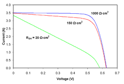
The fill factor is directly affected by the values of the cell's series, shunt resistances and diodes losses. Increasing the shunt resistance (Rsh) and decreasing the series resistance (Rs) lead to a higher fill factor, thus resulting in greater efficiency, and bringing the cell's output power closer to its theoretical maximum.

Typical fill factors range from 50% to 82%. The fill factor for a normal silicon PV cell is 80%.

Comparison

Energy conversion efficiency is measured by dividing the electrical output by the incident light power. Factors influencing output include spectral distribution, spatial distribution of power, temperature, and resistive load. IEC standard 61215 is used to compare the performance of cells and is designed around standard (terrestrial, temperate) temperature and conditions (STC): irradiance of 1 kW/m2, a spectral distribution close to solar radiation through AM (airmass) of 1.5 and a cell temperature 25 °C. The resistive load is varied until the peak or maximum power point (MPP) is achieved. The power at this point is recorded as Watt-peak (Wp). The same standard is used for measuring the power and efficiency of PV modules.

Air mass affects output. In space, where there is no atmosphere, the spectrum of the sun is relatively unfiltered. However, on earth, air filters the incoming light, changing the solar spectrum. The filtering effect ranges from Air Mass 0 (AM0) in space, to approximately Air Mass 1.5 on Earth. Multiplying the spectral differences by the quantum efficiency of the solar cell in question yields the efficiency. Terrestrial efficiencies typically are greater than space efficiencies. For example, a silicon solar cell in space might have an efficiency of 14% at AM0, but 16% on earth at AM 1.5. Note, however, that the number of incident photons in space is considerably larger, so the solar cell might produce considerably more power in space, despite the lower efficiency as indicated by reduced percentage of the total incident energy captured.

Solar cell efficiencies vary from 6% for amorphous silicon-based solar cells to 44.0% with multiple-junction production cells and 44.4% with multiple dies assembled into a hybrid package. Solar cell energy conversion efficiencies for commercially available multicrystalline Si solar cells are around 14–19%. The highest efficiency cells have not always been the most economical – for example a 30% efficient multijunction cell based on exotic materials such as gallium arsenide or indium selenide produced at low volume might well cost one hundred times as much as an 8% efficient amorphous silicon cell in mass production, while delivering only about four times the output.

However, there is a way to "boost" solar power. By increasing the light intensity, typically photogenerated carriers are increased, increasing efficiency by up to 15%. These so-called "concentrator systems" have only begun to become cost-competitive as a result of the development of high efficiency GaAs cells. The increase in intensity is typically accomplished by using concentrating optics. A typical concentrator system may use a light intensity 6–400 times the sun, and increase the efficiency of a one sun GaAs cell from 31% at AM 1.5 to 35%.

A common method used to express economic costs is to calculate a price per delivered kilowatt-hour (kWh). The solar cell efficiency in combination with the available irradiation has a major influence on the costs, but generally speaking the overall system efficiency is important. Commercially available solar cells (as of 2006) reached system efficiencies between 5 and 19%.

Undoped crystalline silicon devices are approaching the theoretical limiting efficiency of 29.43%. In 2017, efficiency of 26.63% was achieved in an amorphous silicon/crystalline silicon heterojunction cell that place both positive and negative contacts on the back of the cell.

Energy payback

The energy payback time is defined as the recovery time required for generating the energy spent for manufacturing a modern photovoltaic module. In 2008, it was estimated to be from 1 to 4 years depending on the module type and location. With a typical lifetime of 20 to 30 years, this means that modern solar cells would be net energy producers, i.e. they would generate more energy over their lifetime than the energy expended in producing them. Generally, thin-film technologies—despite having comparatively low conversion efficiencies—achieve significantly shorter energy payback times than conventional systems (often < 1 year).

A study published in 2013 which the existing literature found that energy payback time was between 0.75 and 3.5 years with thin film cells being at the lower end and multi-si-cells having a payback time of 1.5–2.6 years. A 2015 review assessed the energy payback time and EROI of solar photovoltaics. In this meta study, which uses an insolation of 1700 kWh/m2/year and a system lifetime of 30 years, mean harmonized EROIs between 8.7 and 34.2 were found. Mean harmonized energy payback time varied from 1.0 to 4.1 years. Crystalline silicon devices achieve on average an energy payback period of 2 years.

Like any other technology, solar cell manufacture is dependent on the existence of a complex global industrial manufacturing system. This includes the fabrication systems typically accounted for in estimates of manufacturing energy; the contingent mining, refining and global transportation systems; and other energy intensive support systems including finance, information, and security systems. The difficulty in measuring such energy overhead confers some uncertainty on any estimate of payback times.

Technical methods of improving efficiency

Choosing optimum transparent conductor

The illuminated side of some types of solar cells, thin films, have a transparent conducting film to allow light to enter into the active material and to collect the generated charge carriers. Typically, films with high transmittance and high electrical conductance such as indium tin oxide, conducting polymers or conducting nanowire networks are used for the purpose. There is a trade-off between high transmittance and electrical conductance, thus optimum density of conducting nanowires or conducting network structure should be chosen for high efficiency.

Promoting light scattering in the visible spectrum

Lining the light-receiving surface of the cell with nano-sized metallic studs can substantially increase the cell efficiency. Light reflects off these studs at an oblique angle to the cell, increasing the length of the light path through the cell. This increases the number of photons absorbed by the cell and the amount of current generated.

The main materials used for the nano-studs are silver, gold, and aluminium. Gold and silver are not very efficient, as they absorb much of the light in the visible spectrum, which contains most of the energy present in sunlight, reducing the amount of light reaching the cell. Aluminium absorbs only ultraviolet radiation, and reflects both visible and infra-red light, so energy loss is minimized. Aluminium can increase cell efficiency up to 22% (in lab conditions).

Radiative cooling

An increase in solar cell temperature of approximately 1 °C causes an efficiency decrease of about 0.45%. To prevent this, a transparent silica crystal layer can be applied to solar panels. The silica layer acts as a thermal black body which emits heat as infrared radiation into space, cooling the cell up to 13 °C.

Anti-reflective coatings and textures

Antireflective coatings could result in more destructive interference of incident light waves from the sun. Therefore, all sunlight would be transmitted into the photovoltaic. Texturizing, in which the surface of a solar cell is altered so that the reflected light strikes the surface again, is another technique used to reduce reflection. These surfaces can be created by etching or using lithography. Adding a flat back surface in addition to texturizing the front surface helps to trap the light within the cell, thus providing a longer optical path.

Rear surface passivation

Surface passivation is critical to solar cell efficiency. Many improvements have been made to the front side of mass-produced solar cells, but the aluminium back-surface is impeding efficiency improvements. The efficiency of many solar cells has benefitted by creating so-called passivated emitter and rear cells (PERCs). The chemical deposition of a rear-surface dielectric passivation layer stack that is also made of a thin silica or aluminium oxide film topped with a silicon nitride film helps to improve efficiency in silicon solar cells. This helped increase cell efficiency for commercial Cz-Si wafer material from just over 17% to over 21% by the mid-2010s, and the cell efficiency for quasi-mono-Si to a record 19.9%.

Concepts of the rear surface passivation for silicon solar cells has also been implemented for CIGS solar cells. The rear surface passivation shows the potential to improve the efficiency. Al2O3 and SiO2 have been used as the passivation materials. Nano-sized point contacts on Al2O3 layer and line contacts on SiO2 layer provide the electrical connection of CIGS absorber to the rear electrode Molybdenum. The point contacts on the Al2O3 layer are created by e-beam lithography and the line contacts on the SiO2 layer are created using photolithography. Also, the implementation of the passivation layers does not change the morphology of the CIGS layers. 


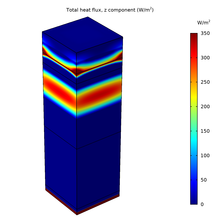
Tot heat flux z.png

Thin film materials

Thin film materials show a lot of promise for solar cells in terms of low costs and adaptability to existing structures and frameworks in technology. Since the materials are so thin, they lack the optical absorption of bulk material solar cells. Attempts to correct this have been tried, more important is thin film surface recombination. Since this is the dominant recombination process of nanoscale thin-film solar cells, it is crucial to their efficiency. Adding a passivating thin layer of silicon dioxide could reduce recombination.

 

Theory of solar cells

From Wikipedia, the free encyclopedia

The theory of solar cells explains the process by which light energy in photons is converted into electric current when the photons strike a suitable semiconductor device. The theoretical studies are of practical use because they predict the fundamental limits of a solar cell, and give guidance on the phenomena that contribute to losses and solar cell efficiency.

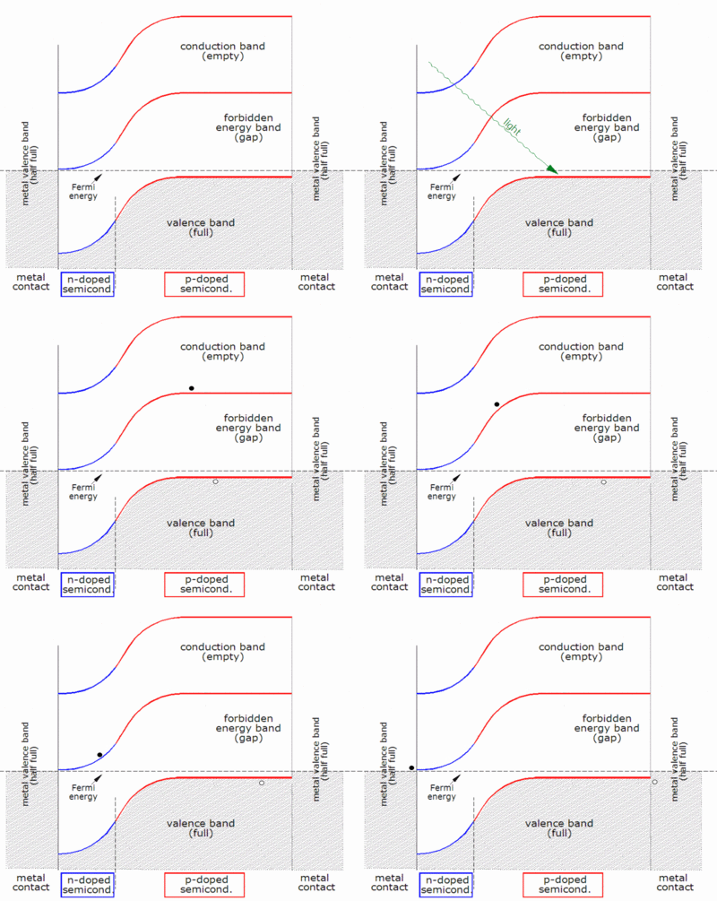
Band diagram of a solar cell, corresponding to very low current (horizontal Fermi level), very low voltage (metal valence bands at same height), and therefore very low illumination

Working explanation

  1. Photons in sunlight hit the solar panel and are absorbed by semi-conducting materials.
  2. Electrons (negatively charged) are knocked loose from their atoms as they are excited. Due to their special structure and the materials in solar cells, the electrons are only allowed to move in a single direction. The electronic structure of the materials is very important for the process to work, and often silicon incorporating small amounts of boron or phosphorus is used in different layers.
  3. An array of solar cells converts solar energy into a usable amount of direct current (DC) electricity.

Photogeneration of charge carriers

When a photon hits a piece of silicon, one of three things can happen:

  1. The photon can pass straight through the silicon — this (generally) happens for lower energy photons.
  2. The photon can reflect off the surface.
  3. The photon can be absorbed by the silicon if the photon energy is higher than the silicon band gap value. This generates an electron-hole pair and sometimes heat depending on the band structure.
Band diagram of a silicon solar cell, corresponding to very low current (horizontal Fermi level), very low voltage (metal valence bands at same height), and therefore very low illumination

When a photon is absorbed, its energy is given to an electron in the crystal lattice. Usually this electron is in the valence band. The energy given to the electron by the photon "excites" it into the conduction band where it is free to move around within the semiconductor. The network of covalent bonds that the electron was previously a part of now has one fewer electron. This is known as a hole. The presence of a missing covalent bond allows the bonded electrons of neighboring atoms to move into the "hole", leaving another hole behind, thus propagating holes throughout the lattice. It can be said that photons absorbed in the semiconductor create electron-hole pairs.

A photon only needs to have energy greater than that of the band gap in order to excite an electron from the valence band into the conduction band. However, the solar frequency spectrum approximates a black body spectrum at about 5,800 K, and as such, much of the solar radiation reaching the Earth is composed of photons with energies greater than the band gap of silicon. These higher energy photons will be absorbed by the solar cell, but the difference in energy between these photons and the silicon band gap is converted into heat (via lattice vibrations — called phonons) rather than into usable electrical energy. The photovoltaic effect can also occur when two photons are absorbed simultaneously in a process called two-photon photovoltaic effect. However, high optical intensities are required for this nonlinear process.

The p-n junction

The most commonly known solar cell is configured as a large-area p-n junction made from silicon. As a simplification, one can imagine bringing a layer of n-type silicon into direct contact with a layer of p-type silicon. In practice, p-n junctions of silicon solar cells are not made in this way, but rather by diffusing an n-type dopant into one side of a p-type wafer (or vice versa).

If a piece of p-type silicon is placed in close contact with a piece of n-type silicon, then a diffusion of electrons occurs from the region of high electron concentration (the n-type side of the junction) into the region of low electron concentration (p-type side of the junction). When the electrons diffuse across the p-n junction, they recombine with holes on the p-type side. However (in the absence of an external circuit) this diffusion of carriers does not go on indefinitely because charges build up on either side of the junction and create an electric field. The electric field promotes charge flow, known as drift current, that opposes and eventually balances out the diffusion of electrons and holes. This region where electrons and holes have diffused across the junction is called the depletion region because it contains practically no mobile charge carriers. It is also known as the space charge region, although space charge extends a bit further in both directions than the depletion region.

Charge carrier separation

There are two causes of charge carrier motion and separation in a solar cell:

  1. drift of carriers, driven by the electric field, with electrons being pushed one way and holes the other way
  2. diffusion of carriers from zones of higher carrier concentration to zones of lower carrier concentration (following a gradient of chemical potential).

These two "forces" may work one against the other at any given point in the cell. For instance, an electron moving through the junction from the p region to the n region (as in the diagram at the beginning of this article) is being pushed by the electric field against the concentration gradient. The same goes for a hole moving in the opposite direction.

It is easiest to understand how a current is generated when considering electron-hole pairs that are created in the depletion zone, which is where there is a strong electric field. The electron is pushed by this field toward the n side and the hole toward the p side. (This is opposite to the direction of current in a forward-biased diode, such as a light-emitting diode in operation.) When the pair is created outside the space charge zone, where the electric field is smaller, diffusion also acts to move the carriers, but the junction still plays a role by sweeping any electrons that reach it from the p side to the n side, and by sweeping any holes that reach it from the n side to the p side, thereby creating a concentration gradient outside the space charge zone.

In thick solar cells there is very little electric field in the active region outside the space charge zone, so the dominant mode of charge carrier separation is diffusion. In these cells the diffusion length of minority carriers (the length that photo-generated carriers can travel before they recombine) must be large compared to the cell thickness. In thin film cells (such as amorphous silicon), the diffusion length of minority carriers is usually very short due to the existence of defects, and the dominant charge separation is therefore drift, driven by the electrostatic field of the junction, which extends to the whole thickness of the cell.

Once the minority carrier enters the drift region, it is 'swept' across the junction and, at the other side of the junction, becomes a majority carrier. This reverse current is a generation current, fed both thermally and (if present) by the absorption of light. On the other hand, majority carriers are driven into the drift region by diffusion (resulting from the concentration gradient), which leads to the forward current; only the majority carriers with the highest energies (in the so-called Boltzmann tail; cf. Maxwell–Boltzmann statistics) can fully cross the drift region. Therefore, the carrier distribution in the whole device is governed by a dynamic equilibrium between reverse current and forward current.

Connection to an external load

Ohmic metal-semiconductor contacts are made to both the n-type and p-type sides of the solar cell, and the electrodes connected to an external load. Electrons that are created on the n-type side, or created on the p-type side, "collected" by the junction and swept onto the n-type side, may travel through the wire, power the load, and continue through the wire until they reach the p-type semiconductor-metal contact. Here, they recombine with a hole that was either created as an electron-hole pair on the p-type side of the solar cell, or a hole that was swept across the junction from the n-type side after being created there.

The voltage measured is equal to the difference in the quasi Fermi levels of the majority carriers (electrons in the n-type portion and holes in the p-type portion) at the two terminals.

Equivalent circuit of a solar cell

The schematic symbol of a solar cell
 
The equivalent circuit of a solar cell

To understand the electronic behavior of a solar cell, it is useful to create a model which is electrically equivalent, and is based on discrete ideal electrical components whose behavior is well defined. An ideal solar cell may be modelled by a current source in parallel with a diode; in practice no solar cell is ideal, so a shunt resistance and a series resistance component are added to the model. The resulting equivalent circuit of a solar cell is shown on the left. Also shown, on the right, is the schematic representation of a solar cell for use in circuit diagrams.

Characteristic equation

From the equivalent circuit it is evident that the current produced by the solar cell is equal to that produced by the current source, minus that which flows through the diode, minus that which flows through the shunt resistor:

where

  • I, output current (ampere)
  • IL, photogenerated current (ampere)
  • ID, diode current (ampere)
  • ISH, shunt current (ampere).

The current through these elements is governed by the voltage across them:

where

  • Vj, voltage across both diode and resistor RSH (volt)
  • V, voltage across the output terminals (volt)
  • I, output current (ampere)
  • RS, series resistance (Ω).

By the Shockley diode equation, the current diverted through the diode is:

where

By Ohm's law, the current diverted through the shunt resistor is:

where

  • RSH, shunt resistance (Ω).

Substituting these into the first equation produces the characteristic equation of a solar cell, which relates solar cell parameters to the output current and voltage:

An alternative derivation produces an equation similar in appearance, but with V on the left-hand side. The two alternatives are identities; that is, they yield precisely the same results.

Since the parameters I0, n, RS, and RSH cannot be measured directly, the most common application of the characteristic equation is nonlinear regression to extract the values of these parameters on the basis of their combined effect on solar cell behavior.

When RS is not zero, the above equation does not give the current I directly, but it can then be solved using the Lambert W function:

When an external load is used with the cell, its resistance can simply be added to RS and V set to zero in order to find the current.

When RSH is infinite there is a solution for V for any less than :

Otherwise one can solve for V using the Lambert W function:

However, when RSH is large it's better to solve the original equation numerically.

The general form of the solution is a curve with I decreasing as V increases (see graphs lower down). The slope at small or negative V (where the W function is near zero) approaches , whereas the slope at high V approaches .

Open-circuit voltage and short-circuit current

When the cell is operated at open circuit, I = 0 and the voltage across the output terminals is defined as the open-circuit voltage. Assuming the shunt resistance is high enough to neglect the final term of the characteristic equation, the open-circuit voltage VOC is:

Similarly, when the cell is operated at short circuit, V = 0 and the current I through the terminals is defined as the short-circuit current. It can be shown that for a high-quality solar cell (low RS and I0, and high RSH) the short-circuit current ISC is:

It is not possible to extract any power from the device when operating at either open circuit or short circuit conditions.

Effect of physical size

The values of IL, I0, RS, and RSH are dependent upon the physical size of the solar cell. In comparing otherwise identical cells, a cell with twice the junction area of another will, in principle, have double the IL and I0 because it has twice the area where photocurrent is generated and across which diode current can flow. By the same argument, it will also have half the RS of the series resistance related to vertical current flow; however, for large-area silicon solar cells, the scaling of the series resistance encountered by lateral current flow is not easily predictable since it will depend crucially on the grid design (it is not clear what "otherwise identical" means in this respect). Depending on the shunt type, the larger cell may also have half the RSH because it has twice the area where shunts may occur; on the other hand, if shunts occur mainly at the perimeter, then RSH will decrease according to the change in circumference, not area.

Since the changes in the currents are the dominating ones and are balancing each other, the open-circuit voltage is practically the same; VOC starts to depend on the cell size only if RSH becomes too low. To account for the dominance of the currents, the characteristic equation is frequently written in terms of current density, or current produced per unit cell area:

where

  • J, current density (ampere/cm2)
  • JL, photogenerated current density (ampere/cm2)
  • J0, reverse saturation current density (ampere/cm2)
  • rS, specific series resistance (Ω·cm2)
  • rSH, specific shunt resistance (Ω·cm2).

This formulation has several advantages. One is that since cell characteristics are referenced to a common cross-sectional area they may be compared for cells of different physical dimensions. While this is of limited benefit in a manufacturing setting, where all cells tend to be the same size, it is useful in research and in comparing cells between manufacturers. Another advantage is that the density equation naturally scales the parameter values to similar orders of magnitude, which can make numerical extraction of them simpler and more accurate even with naive solution methods.

There are practical limitations of this formulation. For instance, certain parasitic effects grow in importance as cell sizes shrink and can affect the extracted parameter values. Recombination and contamination of the junction tend to be greatest at the perimeter of the cell, so very small cells may exhibit higher values of J0 or lower values of RSH than larger cells that are otherwise identical. In such cases, comparisons between cells must be made cautiously and with these effects in mind.

This approach should only be used for comparing solar cells with comparable layout. For instance, a comparison between primarily quadratical solar cells like typical crystalline silicon solar cells and narrow but long solar cells like typical thin film solar cells can lead to wrong assumptions caused by the different kinds of current paths and therefore the influence of, for instance, a distributed series resistance contribution to rS. Macro-architecture of the solar cells could result in different surface areas being placed in any fixed volume - particularly for thin film solar cells and flexible solar cells which may allow for highly convoluted folded structures. If volume is the binding constraint, then efficiency density based on surface area may be of less relevance.

Transparent conducting electrodes

Schematic of charge collection by solar cell electrodes. Light transmits through transparent conducting electrode creating electron hole pairs, which are collected by both the electrodes.

Transparent conducting electrodes are essential components of solar cells. It is either a continuous film of indium tin oxide or a conducting wire network, in which wires are charge collectors while voids between wires are transparent for light. An optimum density of wire network is essential for the maximum solar cell performance as higher wire density blocks the light transmittance while lower wire density leads to high recombination losses due to more distance traveled by the charge carriers.

Cell temperature

Effect of temperature on the current-voltage characteristics of a solar cell

Temperature affects the characteristic equation in two ways: directly, via T in the exponential term, and indirectly via its effect on I0 (strictly speaking, temperature affects all of the terms, but these two far more significantly than the others). While increasing T reduces the magnitude of the exponent in the characteristic equation, the value of I0 increases exponentially with T. The net effect is to reduce VOC (the open-circuit voltage) linearly with increasing temperature. The magnitude of this reduction is inversely proportional to VOC; that is, cells with higher values of VOC suffer smaller reductions in voltage with increasing temperature. For most crystalline silicon solar cells the change in VOC with temperature is about −0.50%/°C, though the rate for the highest-efficiency crystalline silicon cells is around −0.35%/°C. By way of comparison, the rate for amorphous silicon solar cells is −0.20 to −0.30%/°C, depending on how the cell is made.

The amount of photogenerated current IL increases slightly with increasing temperature because of an increase in the number of thermally generated carriers in the cell. This effect is slight, however: about 0.065%/°C for crystalline silicon cells and 0.09% for amorphous silicon cells.

The overall effect of temperature on cell efficiency can be computed using these factors in combination with the characteristic equation. However, since the change in voltage is much stronger than the change in current, the overall effect on efficiency tends to be similar to that on voltage. Most crystalline silicon solar cells decline in efficiency by 0.50%/°C and most amorphous cells decline by 0.15−0.25%/°C. The figure above shows I-V curves that might typically be seen for a crystalline silicon solar cell at various temperatures.

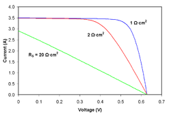
Series resistance

Effect of series resistance on the current-voltage characteristics of a solar cell

As series resistance increases, the voltage drop between the junction voltage and the terminal voltage becomes greater for the same current. The result is that the current-controlled portion of the I-V curve begins to sag toward the origin, producing a significant decrease in the terminal voltage V and a slight reduction in ISC, the short-circuit current. Very high values of RS will also produce a significant reduction in ISC; in these regimes, series resistance dominates and the behavior of the solar cell resembles that of a resistor. These effects are shown for crystalline silicon solar cells in the I-V curves displayed in the figure to the right.

Losses caused by series resistance are in a first approximation given by Ploss = VRsI = I2RS and increase quadratically with (photo-)current. Series resistance losses are therefore most important at high illumination intensities.

Shunt resistance

Effect of shunt resistance on the current–voltage characteristics of a solar cell

As shunt resistance decreases, the current diverted through the shunt resistor increases for a given level of junction voltage. The result is that the voltage-controlled portion of the I-V curve begins to sag far from the origin, producing a significant decrease in the terminal current I and a slight reduction in VOC. Very low values of RSH will produce a significant reduction in VOC. Much as in the case of a high series resistance, a badly shunted solar cell will take on operating characteristics similar to those of a resistor. These effects are shown for crystalline silicon solar cells in the I-V curves displayed in the figure to the right.

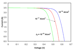
Reverse saturation current

Effect of reverse saturation current on the current-voltage characteristics of a solar cell

If one assumes infinite shunt resistance, the characteristic equation can be solved for VOC:

Thus, an increase in I0 produces a reduction in VOC proportional to the inverse of the logarithm of the increase. This explains mathematically the reason for the reduction in VOC that accompanies increases in temperature described above. The effect of reverse saturation current on the I-V curve of a crystalline silicon solar cell are shown in the figure to the right. Physically, reverse saturation current is a measure of the "leakage" of carriers across the p-n junction in reverse bias. This leakage is a result of carrier recombination in the neutral regions on either side of the junction.

Ideality factor

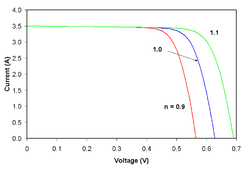
Effect of ideality factor on the current-voltage characteristics of a solar cell

The ideality factor (also called the emissivity factor) is a fitting parameter that describes how closely the diode's behavior matches that predicted by theory, which assumes the p-n junction of the diode is an infinite plane and no recombination occurs within the space-charge region. A perfect match to theory is indicated when n = 1. When recombination in the space-charge region dominate other recombination, however, n = 2. The effect of changing ideality factor independently of all other parameters is shown for a crystalline silicon solar cell in the I-V curves displayed in the figure to the right.

Most solar cells, which are quite large compared to conventional diodes, well approximate an infinite plane and will usually exhibit near-ideal behavior under standard test conditions (n ≈ 1). Under certain operating conditions, however, device operation may be dominated by recombination in the space-charge region. This is characterized by a significant increase in I0 as well as an increase in ideality factor to n ≈ 2. The latter tends to increase solar cell output voltage while the former acts to erode it. The net effect, therefore, is a combination of the increase in voltage shown for increasing n in the figure to the right and the decrease in voltage shown for increasing I0 in the figure above. Typically, I0 is the more significant factor and the result is a reduction in voltage.

Sometimes, the ideality factor is observed to be greater than 2, which is generally attributed to the presence of Schottky diode or heterojunction in the solar cell. The presence of a heterojunction offset reduces the collection efficiency of the solar cell and may contribute to low fill-factor.

Cooperative

From Wikipedia, the free encyclopedia ...