Search This Blog

Sunday, July 1, 2018

Carbon nanotube

From Wikipedia, the free encyclopedia


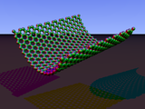
Rotating single-walled zigzag carbon nanotube

Carbon nanotubes (CNTs) are allotropes of carbon with a cylindrical nanostructure. These cylindrical carbon molecules have unusual properties, which are valuable for nanotechnology, electronics, optics and other fields of materials science and technology. Owing to the material's exceptional strength and stiffness, nanotubes have been constructed with length-to-diameter ratio of up to 132,000,000:1,[1] significantly larger than for any other material.

In addition, owing to their extraordinary thermal conductivity, mechanical, and electrical properties, carbon nanotubes find applications as additives to various structural materials. For instance, nanotubes form a tiny portion of the material(s) in some (primarily carbon fiber) baseball bats, golf clubs, car parts or damascus steel.[2][3]

Nanotubes are members of the fullerene structural family. Their name is derived from their long, hollow structure with the walls formed by one-atom-thick sheets of carbon, called graphene. These sheets are rolled at specific and discrete ("chiral") angles, and the combination of the rolling angle and radius decides the nanotube properties; for example, whether the individual nanotube shell is a metal or semiconductor. Nanotubes are categorized as single-walled nanotubes (SWNTs) and multi-walled nanotubes (MWNTs). Individual nanotubes naturally align themselves into "ropes" held together by van der Waals forces, more specifically, pi-stacking.

Applied quantum chemistry, specifically, orbital hybridization best describes chemical bonding in nanotubes. The chemical bonding of nanotubes involves entirely sp2-hybrid carbon atoms. These bonds, which are similar to those of graphite and stronger than those found in alkanes and diamond (which employ sp3-hybrid carbon atoms), provide nanotubes with their unique strength.

Types of carbon nanotubes and related structures

There is no consensus on some terms describing carbon nanotubes in scientific literature: both "-wall" and "-walled" are being used in combination with "single", "double", "triple" or "multi", and the letter C is often omitted in the abbreviation; for example, multi-walled carbon nanotube (MWNT).

Single-walled


The (n,m) nanotube naming scheme can be thought of as a vector (Ch) in an infinite graphene sheet that describes how to "roll up" the graphene sheet to make the nanotube. T denotes the tube axis, and a1 and a2 are the unit vectors of graphene in real space.

A scanning tunneling microscopy image of single-walled carbon nanotube

A transmission electron microscopy image of a single-walled carbon nanotube
d={\frac {a}{\pi }}{\sqrt {(n^{2}+nm+m^{2})}}=78.3{\sqrt {((n+m)^{2}-nm)}}{\rm {pm,}}
where a = 0.246 nm.

SWNTs are an important variety of carbon nanotube because most of their properties change significantly with the (n,m) values, and this dependence is non-monotonic (see Kataura plot). In particular, their band gap can vary from zero to about 2 eV and their electrical conductivity can show metallic or semiconducting behavior. Single-walled nanotubes are likely candidates for miniaturizing electronics. The most basic building block of these systems is the electric wire, and SWNTs with diameters of an order of a nanometer can be excellent conductors.[4][5] One useful application of SWNTs is in the development of the first intermolecular field-effect transistors (FET). The first intermolecular logic gate using SWCNT FETs was made in 2001.[6] A logic gate requires both a p-FET and an n-FET. Because SWNTs are p-FETs when exposed to oxygen and n-FETs otherwise, it is possible to expose half of an SWNT to oxygen and protect the other half from it. The resulting SWNT acts as a not logic gate with both p and n-type FETs in the same molecule.

Prices for single-walled nanotubes declined from around $1500 per gram as of 2000 to retail prices of around $50 per gram of as-produced 40–60% by weight SWNTs as of March 2010. As of 2016 the retail price of as-produced 75% by weight SWNTs were $2 per gram, cheap enough for widespread use.[7] SWNTs are forecast to make a large impact in electronics applications by 2020 according to The Global Market for Carbon Nanotubes report.

Multi-walled


A scanning electron microscopy image of carbon nanotubes bundles

Triple-walled armchair carbon nanotube

Multi-walled nanotubes (MWNTs) consist of multiple rolled layers (concentric tubes) of graphene. There are two models that can be used to describe the structures of multi-walled nanotubes. In the Russian Doll model, sheets of graphite are arranged in concentric cylinders, e.g., a (0,8) single-walled nanotube (SWNT) within a larger (0,17) single-walled nanotube. In the Parchment model, a single sheet of graphite is rolled in around itself, resembling a scroll of parchment or a rolled newspaper. The interlayer distance in multi-walled nanotubes is close to the distance between graphene layers in graphite, approximately 3.4 Å. The Russian Doll structure is observed more commonly. Its individual shells can be described as SWNTs, which can be metallic or semiconducting. Because of statistical probability and restrictions on the relative diameters of the individual tubes, one of the shells, and thus the whole MWNT, is usually a zero-gap metal.

Double-walled carbon nanotubes (DWNTs) form a special class of nanotubes because their morphology and properties are similar to those of SWNTs but they are more resistant to chemicals.[citation needed] This is especially important when it is necessary to graft chemical functions to the surface of the nanotubes (functionalization) to add properties to the CNT. Covalent functionalization of SWNTs will break some C=C double bonds, leaving "holes" in the structure on the nanotube, and thus modifying both its mechanical and electrical properties. In the case of DWNTs, only the outer wall is modified. DWNT synthesis on the gram-scale was first proposed in 2003[8] by the CCVD technique, from the selective reduction of oxide solutions in methane and hydrogen.

The telescopic motion ability of inner shells[9] and their unique mechanical properties[10] will permit the use of multi-walled nanotubes as main movable arms in coming nanomechanical devices. Retraction force that occurs to telescopic motion caused by the Lennard-Jones interaction between shells and its value is about 1.5 nN.[11]

Junctions and crosslinking


Transmission electron microscope image of carbon nanotube junction

Junctions between 2 or more nanotubes have been widely discussed theoretically.[12][13] Such junctions are quite frequently observed in samples prepared by arc discharge as well as by chemical vapor deposition. The electronic properties of such junctions were first considered theoretically by Lambin et al.,[14] who pointed out that a connection between metallic tube and a semiconducting one would represent a nanoscale heterojunction. Such a junction could therefore form a component of a nanotube-based electronic circuit. The image on the right shows a junction between two multiwalled nanotubes. Junctions between nanotubes and graphene have been considered theoretically,[15] but not widely studied experimentally. Such junctions form the basis of pillared graphene, in which parallel graphene sheets are separated by short nanotubes.[16] Pillared graphene represents a class of three-dimensional carbon nanotube architectures.


3D carbon scaffolds

Recently, several studies have highlighted the prospect of using carbon nanotubes as building blocks to fabricate three-dimensional macroscopic (>100 nm in all three dimensions) all-carbon devices. Lalwani et al. have reported a novel radical initiated thermal crosslinking method to fabricate macroscopic, free-standing, porous, all-carbon scaffolds using single- and multi-walled carbon nanotubes as building blocks.[17] These scaffolds possess macro-, micro-, and nano- structured pores and the porosity can be tailored for specific applications. These 3D all-carbon scaffolds/architectures may be used for the fabrication of the next generation of energy storage, supercapacitors, field emission transistors, high-performance catalysis, photovoltaics, and biomedical devices and implants.[18]

Other morphologies


A stable nanobud structure

Carbon nanobuds are a newly created material combining two previously discovered allotropes of carbon: carbon nanotubes and fullerenes. In this new material, fullerene-like "buds" are covalently bonded to the outer sidewalls of the underlying carbon nanotube. This hybrid material has useful properties of both fullerenes and carbon nanotubes. In particular, they have been found to be exceptionally good field emitters.[19] In composite materials, the attached fullerene molecules may function as molecular anchors preventing slipping of the nanotubes, thus improving the composite’s mechanical properties.

A carbon peapod[20][21] is a novel hybrid carbon material which traps fullerene inside a carbon nanotube. It can possess interesting magnetic properties with heating and irradiation. It can also be applied as an oscillator during theoretical investigations and predictions.[22][23]

In theory, a nanotorus is a carbon nanotube bent into a torus (doughnut shape). Nanotori are predicted to have many unique properties, such as magnetic moments 1000 times larger than previously expected for certain specific radii.[24] Properties such as magnetic moment, thermal stability, etc. vary widely depending on radius of the torus and radius of the tube.[24][25]

Graphenated carbon nanotubes are a relatively new hybrid that combines graphitic foliates grown along the sidewalls of multiwalled or bamboo style CNTs. The foliate density can vary as a function of deposition conditions (e.g. temperature and time) with their structure ranging from few layers of graphene (< 10) to thicker, more graphite-like.[26] The fundamental advantage of an integrated graphene-CNT structure is the high surface area three-dimensional framework of the CNTs coupled with the high edge density of graphene. Depositing a high density of graphene foliates along the length of aligned CNTs can significantly increase the total charge capacity per unit of nominal area as compared to other carbon nanostructures.[27]

Cup-stacked carbon nanotubes (CSCNTs) differ from other quasi-1D carbon structures, which normally behave as quasi-metallic conductors of electrons. CSCNTs exhibit semiconducting behaviors due to the stacking microstructure of graphene layers.[28]

Extreme carbon nanotubes


Cycloparaphenylene

The observation of the longest carbon nanotubes grown so far are over 1/2 m (550 mm long) was reported in 2013.[29] These nanotubes were grown on silicon substrates using an improved chemical vapor deposition (CVD) method and represent electrically uniform arrays of single-walled carbon nanotubes.[1]

The shortest carbon nanotube is the organic compound cycloparaphenylene, which was synthesized in 2008.[30]

The thinnest carbon nanotube is the armchair (2,2) CNT with a diameter of 0.3 nm. This nanotube was grown inside a multi-walled carbon nanotube. Assigning of carbon nanotube type was done by a combination of high-resolution transmission electron microscopy (HRTEM), Raman spectroscopy and density functional theory (DFT) calculations.[31]

The thinnest freestanding single-walled carbon nanotube is about 0.43 nm in diameter[32]. Researchers suggested that it can be either (5,1) or (4,2) SWCNT, but the exact type of carbon nanotube remains questionable.[33] (3,3), (4,3) and (5,1) carbon nanotubes (all about 0.4 nm in diameter) were unambiguously identified using aberration-corrected high-resolution transmission electron microscopy inside double-walled CNTs.[34]

The highest density of CNTs was achieved in 2013, grown on a conductive titanium-coated copper surface that was coated with co-catalysts cobalt and molybdenum at lower than typical temperatures of 450 °C. The tubes averaged a height of 380 nm and a mass density of 1.6 g cm−3. The material showed ohmic conductivity (lowest resistance ∼22 kΩ).[35][36]

Properties

Mechanical

Carbon nanotubes are the strongest and stiffest materials yet discovered in terms of tensile strength and elastic modulus respectively. This strength results from the covalent sp2 bonds formed between the individual carbon atoms. In 2000, a multi-walled carbon nanotube was tested to have a tensile strength of 63 gigapascals (9,100,000 psi).[37] (For illustration, this translates into the ability to endure tension of a weight equivalent to 6,422 kilograms-force (62,980 N; 14,160 lbf) on a cable with cross-section of 1 square millimetre (0.0016 sq in).) Further studies, such as one conducted in 2008, revealed that individual CNT shells have strengths of up to ≈100 gigapascals (15,000,000 psi), which is in agreement with quantum/atomistic models.[38] Since carbon nanotubes have a low density for a solid of 1.3 to 1.4 g/cm3,[39] its specific strength of up to 48,000 kN·m·kg−1 is the best of known materials, compared to high-carbon steel's 154 kN·m·kg−1.

Although the strength of individual CNT shells is extremely high, weak shear interactions between adjacent shells and tubes lead to significant reduction in the effective strength of multi-walled carbon nanotubes and carbon nanotube bundles down to only a few GPa.[40] This limitation has been recently addressed by applying high-energy electron irradiation, which crosslinks inner shells and tubes, and effectively increases the strength of these materials to ≈60 GPa for multi-walled carbon nanotubes[38] and ≈17 GPa for double-walled carbon nanotube bundles.[40] CNTs are not nearly as strong under compression. Because of their hollow structure and high aspect ratio, they tend to undergo buckling when placed under compressive, torsional, or bending stress.[41]

On the other hand, there was evidence that in the radial direction they are rather soft. The first transmission electron microscope observation of radial elasticity suggested that even the van der Waals forces can deform two adjacent nanotubes. Later, nanoindentations with atomic force microscope were performed by several groups to quantitatively measure radial elasticity of multiwalled carbon nanotubes and tapping/contact mode atomic force microscopy was also performed on single-walled carbon nanotubes. Young's modulus of on the order of several GPa showed that CNTs are in fact very soft in the radial direction.

Electrical


Band structures computed using tight binding approximation for (6,0) CNT (zigzag, metallic), (10,2) CNT (semiconducting) and (10,10) CNT (armchair, metallic).

Unlike graphene, which is a two-dimensional semimetal, carbon nanotubes are either metallic or semiconducting along the tubular axis. For a given (n,m) nanotube, if n = m, the nanotube is metallic; if nm is a multiple of 3 and n ≠ m and nm ≠ 0, then the nanotube is quasi-metallic with a very small band gap, otherwise the nanotube is a moderate semiconductor. [42] Thus all armchair (n = m) nanotubes are metallic, and nanotubes (6,4), (9,1), etc. are semiconducting.[43] Carbon nanotubes are not semimetallic because the degenerate point (that point where the π [bonding] band meets the π* [anti-bonding] band, at which the energy goes to zero) is slightly shifted away from the K point in the Brillouin zone due to the curvature of the tube surface, causing hybridization between the σ* and π* anti-bonding bands, modifying the band dispersion.

The rule regarding metallic versus semiconductor behavior has exceptions, because curvature effects in small diameter tubes can strongly influence electrical properties. Thus, a (5,0) SWCNT that should be semiconducting in fact is metallic according to the calculations. Likewise, zigzag and chiral SWCNTs with small diameters that should be metallic have a finite gap (armchair nanotubes remain metallic).[43] In theory, metallic nanotubes can carry an electric current density of 4 × 10⁹ A/cm2, which is more than 1,000 times greater than those of metals such as copper,[44] where for copper interconnects current densities are limited by electromigration. Carbon nanotubes are thus being explored as interconnects, conductivity enhancing components in composite materials and many groups are attempting to commercialize highly conducting electrical wire assembled from individual carbon nanotubes. There are significant challenges to be overcome, however, such as undesired current saturation under voltage,[45] the much more resistive nanotube-to-nanotube junctions and impurities, all of which lower the electrical conductivity of the macroscopic nanotube wires by orders of magnitude, as compared to the conductivity of the individual nanotubes.

Because of its nanoscale cross-section, electrons propagate only along the tube's axis. As a result, carbon nanotubes are frequently referred to as one-dimensional conductors. The maximum electrical conductance of a single-walled carbon nanotube is 2G0, where G0 = 2e2/h is the conductance of a single ballistic quantum channel.[46]

Due to the role of the π-electron system in determining the electronic properties of graphene, doping in carbon nanotubes differs from that of bulk crystalline semiconductors from the same group of the periodic table (e.g. silicon). Graphitic substitution of carbon atoms in the nanotube wall by boron or nitrogen dopants leads to p-type and n-type behavior, respectively, as would be expected in silicon. However, some non-substitutional (intercalated or adsorbed) dopants introduced into a carbon nanotube, such as alkali metals as well as electron-rich metallocenes, result in n-type conduction because they donate electrons to the π-electron system of the nanotube. By contrast, π-electron acceptors such as FeCl3 or electron-deficient metallocenes function as p-type dopants since they draw π-electrons away from the top of the valence band.

Intrinsic superconductivity has been reported,[47] although other experiments found no evidence of this, leaving the claim a subject of debate.[48]

Optical

Carbon nanotubes have useful absorption, photoluminescence (fluorescence), and Raman spectroscopy properties. Spectroscopic methods offer the possibility of quick and non-destructive characterization of relatively large amounts of carbon nanotubes. There is a strong demand for such characterization from the industrial point of view: numerous parameters of the nanotube synthesis can be changed, intentionally or unintentionally, to alter the nanotube quality. As shown below, optical absorption, photoluminescence and Raman spectroscopies allow quick and reliable characterization of this "nanotube quality" in terms of non-tubular carbon content, structure (chirality) of the produced nanotubes, and structural defects. Those features determine nearly any other properties such as optical, mechanical, and electrical properties.

Carbon nanotubes are unique "one-dimensional systems" which can be envisioned as rolled single sheets of graphite (or more precisely graphene). This rolling can be done at different angles and curvatures resulting in different nanotube properties. The diameter typically varies in the range 0.4–40 nm (i.e. "only" ~100 times), but the length can vary ~100,000,000,000 times, from 0.14 nm to 55.5 cm.[49] The nanotube aspect ratio, or the length-to-diameter ratio, can be as high as 132,000,000:1,[50] which is unequalled by any other material. Consequently, all the properties of the carbon nanotubes relative to those of typical semiconductors are extremely anisotropic (directionally dependent) and tunable.

Whereas mechanical, electrical and electrochemical (supercapacitor) properties of the carbon nanotubes are well established and have immediate applications, the practical use of optical properties is yet unclear. The aforementioned tunability of properties is potentially useful in optics and photonics. In particular, light-emitting diodes (LEDs)[51][52] and photo-detectors[53] based on a single nanotube have been produced in the lab. Their unique feature is not the efficiency, which is yet relatively low, but the narrow selectivity in the wavelength of emission and detection of light and the possibility of its fine tuning through the nanotube structure. In addition, bolometer[54] and optoelectronic memory[55] devices have been realised on ensembles of single-walled carbon nanotubes.

Crystallographic defects also affect the tube's electrical properties. A common result is lowered conductivity through the defective region of the tube. A defect in armchair-type tubes (which can conduct electricity) can cause the surrounding region to become semiconducting, and single monatomic vacancies induce magnetic properties.[56]

Thermal

All nanotubes are expected to be very good thermal conductors along the tube, exhibiting a property known as "ballistic conduction", but good insulators lateral to the tube axis. Measurements show that an individual SWNT has a room-temperature thermal conductivity along its axis of about 3500 W·m−1·K−1;[57] compare this to copper, a metal well known for its good thermal conductivity, which transmits 385 W·m−1·K−1. An individual SWNT has a room-temperature thermal conductivity across its axis (in the radial direction) of about 1.52 W·m−1·K−1,[58] which is about as thermally conductive as soil. Macroscopic assemblies of nanotubes such as films or fibres have reached up to 1500 W·m−1·K−1 so far.[59] The temperature stability of carbon nanotubes is estimated to be up to 2800 °C in vacuum and about 750 °C in air.[60]

Crystallographic defects strongly affect the tube's thermal properties. Such defects lead to phonon scattering, which in turn increases the relaxation rate of the phonons. This reduces the mean free path and reduces the thermal conductivity of nanotube structures. Phonon transport simulations indicate that substitutional defects such as nitrogen or boron will primarily lead to scattering of high-frequency optical phonons. However, larger-scale defects such as Stone Wales defects cause phonon scattering over a wide range of frequencies, leading to a greater reduction in thermal conductivity.[61]

Synthesis

Techniques have been developed to produce nanotubes in sizable quantities, including arc discharge, laser ablation, chemical vapor deposition (CVD) and high-pressure carbon monoxide disproportionation (HiPCO). Among these arc discharge, laser ablation, chemical vapor deposition (CVD) are batch by batch process and HiPCO is gas phase continuous process.[62] Most of these processes take place in a vacuum or with process gases. The CVD growth method is popular, as it yields high quantity and has a degree of control over diameter, length and morphology. Using particulate catalysts, large quantities of nanotubes can be synthesized by these methods, but achieving the repeatability becomes a major problem with CVD growth.[63] The HiPCO process advances in catalysis and continuous growth are making CNTs more commercially viable.[64] The HiPCO process helps in producing high purity single walled carbon nanotubes in higher quantity. The HiPCO reactor operates at high temperature 900-1100°C and high pressure ~30-50 bar.[65] It uses carbon monoxide as the carbon source and Nickel/ iron penta carbonyl as catalyst. These catalyst acts as the nucleation site for the nanotubes to grow.[62]

Vertically aligned carbon nanotube arrays are also grown by thermal chemical vapor deposition. A substrate (quartz, silicon, stainless steel, etc.) is coated with a catalytic metal (Fe, Co, Ni) layer. Typically that layer is iron, and is deposited via sputtering to a thickness of 1–5 nm. A 10–50 nm underlayer of alumina is often also put down on the substrate first. This imparts controllable wetting and good interfacial properties. When the substrate is heated to the growth temperature (~700 °C), the continuous iron film breaks up into small islands… each island then nucleates a carbon nanotube. The sputtered thickness controls the island size, and this in turn determines the nanotube diameter. Thinner iron layers drive down the diameter of the islands, and they drive down the diameter of the nanotubes grown. The amount of time that the metal island can sit at the growth temperature is limited, as they are mobile, and can merge into larger (but fewer) islands. Annealing at the growth temperature reduces the site density (number of CNT/mm2) while increasing the catalyst diameter.

The as-prepared carbon nanotubes always have impurities such as other forms of carbon (amorphous carbon, fullerene, etc.) and non-carbonaceous impurities (metal pes used for catalyst).[66][67] These impurities need to be removed to make use of the carbon nanotubes in applications.[68]

Metrology

There are many metrology standards and reference materials available for carbon nanotubes.[69]
For single-wall carbon nanotubes, ISO/TS 10868 describes a measurement method for the diameter, purity, and fraction of metallic nanotubes through optical absorption spectroscopy,[70] while ISO/TS 10797 and ISO/TS 10798 establish methods to characterize the morphology and elemental composition of single-wall carbon nanotubes, using transmission electron microscopy and scanning electron microscopy respectively, coupled with energy dispersive X-ray spectrometry analysis.[71][72]
NIST SRM 2483 is a soot of single-wall carbon nanotubes used as a reference material for elemental analysis, and was characterized using thermogravimetric analysis, prompt gamma activation analysis, induced neutron activation analysis, inductively coupled plasma mass spectroscopy, resonant Raman scattering, UV-visible-near infrared fluorescence spectroscopy and absorption spectroscopy, scanning electron microscopy, and transmission electron microscopy.[73][74] The Canadian National Research Council also offers a certified reference material SWCNT-1 for elemental analysis using neutron activation analysis and inductively coupled plasma mass spectroscopy.[69][75] NIST RM 8281 is a mixture of three lengths of single-wall carbon nanotube.[73][76]

For multiwall carbon nanotubes, ISO/TR 10929 identifies the basic properties and the content of impurities,[77] while ISO/TS 11888 describes morphology using scanning electron microscopy, transmission electron microscopy, viscometry, and light scattering analysis.[78] ISO/TS 10798 is also valid for multiwall carbon nanotubes.[72]

Chemical modification

Carbon nanotubes can be functionalized to attain desired properties that can be used in a wide variety of applications. The two main methods of carbon nanotube functionalization are covalent and non-covalent modifications. Because of their hydrophobic nature, carbon nanotubes tend to agglomerate hindering their dispersion in solvents or viscous polymer melts. The resulting nanotube bundles or aggregates reduce the mechanical performance of the final composite. The surface of the carbon nanotubes can be modified to reduce the hydrophobicity and improve interfacial adhesion to a bulk polymer through chemical attachment.[79]

Applications

Current

Current use and application of nanotubes has mostly been limited to the use of bulk nanotubes, which is a mass of rather unorganized fragments of nanotubes. Bulk nanotube materials may never achieve a tensile strength similar to that of individual tubes, but such composites may, nevertheless, yield strengths sufficient for many applications. Bulk carbon nanotubes have already been used as composite fibers in polymers to improve the mechanical, thermal and electrical properties of the bulk product.
  • Easton-Bell Sports, Inc. have been in partnership with Zyvex Performance Materials, using CNT technology in a number of their bicycle components – including flat and riser handlebars, cranks, forks, seatposts, stems and aero bars.
  • Zyvex Technologies has also built a 54' maritime vessel, the Piranha Unmanned Surface Vessel, as a technology demonstrator for what is possible using CNT technology. CNTs help improve the structural performance of the vessel, resulting in a lightweight 8,000 lb boat that can carry a payload of 15,000 lb over a range of 2,500 miles.[80]
  • Amroy Europe Oy manufactures Hybtonite carbon nanoepoxy resins where carbon nanotubes have been chemically activated to bond to epoxy, resulting in a composite material that is 20% to 30% stronger than other composite materials. It has been used for wind turbines, marine paints and a variety of sports gear such as skis, ice hockey sticks, baseball bats, hunting arrows, and surfboards.[81]
  • The Boeing Company has patented the use of carbon nanotubes for structural health monitoring[82] of composites used in aircraft structures. This technology will greatly reduce the risk of an in-flight failure caused by structural degradation of aircraft.
Other current applications include:
Current research for modern applications include:
  • using carbon nanotubes as a scaffold for diverse microfabrication techniques.[85]
  • energy dissipation in self-organized nanostructures under influence of an electric field.[86]
  • using carbon nanotubes for environmental monitoring due to their active surface area and their ability to absorb gases.[87]

Potential

The strength and flexibility of carbon nanotubes makes them of potential use in controlling other nanoscale structures, which suggests they will have an important role in nanotechnology engineering. The highest tensile strength of an individual multi-walled carbon nanotube has been tested to be 63 GPa.[37] Carbon nanotubes were found in Damascus steel from the 17th century, possibly helping to account for the legendary strength of the swords made of it.[88][89] Recently, several studies have highlighted the prospect of using carbon nanotubes as building blocks to fabricate three-dimensional macroscopic (>1mm in all three dimensions) all-carbon devices. Lalwani et al. have reported a novel radical initiated thermal crosslinking method to fabricated macroscopic, free-standing, porous, all-carbon scaffolds using single- and multi-walled carbon nanotubes as building blocks.[17] These scaffolds possess macro-, micro-, and nano- structured pores and the porosity can be tailored for specific applications. These 3D all-carbon scaffolds/architectures may be used for the fabrication of the next generation of energy storage, supercapacitors, field emission transistors, high-performance catalysis,[90] photovoltaics, and biomedical devices and implants.

CNTs are potential candidates for future via and wire material in nano-scale VLSI circuits. Eliminating electromigration reliability concerns that plague todays Cu interconnects, isolated (single and multi-wall) CNTs can carry current densities in excess of 1000 MA/sq-cm without electromigration damage.[91]

Large quantities of pure CNTs can be made into a freestanding sheet or film by surface-engineered tape-casting (SETC) fabrication technique which is a scalable method to fabricate flexible and foldable sheets with superior properties.[92][93] Another reported form factor is CNT fiber (a.k.a. filament) by wet spinning.[94] The fiber is either directly spun from the synthesis pot or spun from pre-made dissolved CNTs. Individual fibers can be turned into a yarn. Apart from its strength and flexibility, the main advantage is making an electrically conducting yarn. The electronic properties of individual CNT fibers (i.e. bundle of individual CNT) are governed by the two-dimensional structure of CNTs. The fibers were measured to have a resistivity only one order of magnitude higher than metallic conductors at 300K. By further optimizing the CNTs and CNT fibers, CNT fibers with improved electrical properties could be developed.[91][95]

CNT-based yarns are suitable for applications in energy and electrochemical water treatment when coated with an ion-exchange membrane.[96] Also, CNT-based yarns could replace copper as a winding material. Pyrhönen et al. (2015) have built a motor using CNT winding.[97][98]

Safety and health

The National Institute for Occupational Safety and Health (NIOSH) is the leading United States federal agency conducting research and providing guidance on the occupational safety and health implications and applications of nanotechnology. Early scientific studies have indicated that some of these nanoscale particles may pose a greater health risk than the larger bulk form of these materials. In 2013, NIOSH published a Current Intelligence Bulletin detailing the potential hazards and recommended exposure limit for carbon nanotubes and fibers.[99]

As of October 2016, single wall carbon nanotubes have been registered through the European Union's Registration, Evaluation, Authorization and Restriction of Chemicals (REACH) regulations, based on evaluation of the potentially hazardous properties of SWCNT. Based on this registration, SWCNT commercialization is allowed in the EU up to 10 metric tons. Currently, the type of SWCNT registered through REACH is limited to the specific type of single wall carbon nanotubes manufactured by OCSiAl, which submitted the application.[100]

History

The true identity of the discoverers of carbon nanotubes is a subject of some controversy.[101] A 2006 editorial written by Marc Monthioux and Vladimir Kuznetsov in the journal Carbon described the interesting and often-misstated origin of the carbon nanotube.[102] A large percentage of academic and popular literature attributes the discovery of hollow, nanometer-size tubes composed of graphitic carbon to Sumio Iijima of NEC in 1991. He published a paper describing his discovery which initiated a flurry of excitement and could be credited by inspiring the many scientists now studying applications of carbon nanotubes. Though Iijima has been given much of the credit for discovering carbon nanotubes, it turns out that the timeline of carbon nanotubes goes back much further than 1991.[101]

In 1952, L. V. Radushkevich and V. M. Lukyanovich published clear images of 50 nanometer diameter tubes made of carbon in the Soviet Journal of Physical Chemistry.[103] This discovery was largely unnoticed, as the article was published in Russian, and Western scientists' access to Soviet press was limited during the Cold War. Monthioux and Kuznetsov mentioned in their Carbon editorial:[102]
The fact is, Radushkevich and Lukyanovich [..] should be credited for the discovery that carbon filaments could be hollow and have a nanometer- size diameter, that is to say for the discovery of carbon nanotubes.
In 1976, Morinobu Endo of CNRS observed hollow tubes of rolled up graphite sheets synthesised by a chemical vapour-growth technique.[104] The first specimens observed would later come to be known as single-walled carbon nanotubes (SWNTs).[105] Endo, in his early review of vapor-phase-grown carbon fibers (VPCF), also reminded us that he had observed a hollow tube, linearly extended with parallel carbon layer faces near the fiber core.[106] This appears to be the observation of multi-walled carbon nanotubes at the center of the fiber.[105] The mass-produced MWCNTs today are strongly related to the VPGCF developed by Endo.[105] In fact, they call it the “Endo-process”, out of respect for his early work and patents.[105][107]

In 1979, John Abrahamson presented evidence of carbon nanotubes at the 14th Biennial Conference of Carbon at Pennsylvania State University. The conference paper described carbon nanotubes as carbon fibers that were produced on carbon anodes during arc discharge. A characterization of these fibers was given as well as hypotheses for their growth in a nitrogen atmosphere at low pressures.[108]

In 1981, a group of Soviet scientists published the results of chemical and structural characterization of carbon nanoparticles produced by a thermocatalytical disproportionation of carbon monoxide. Using TEM images and XRD patterns, the authors suggested that their “carbon multi-layer tubular crystals” were formed by rolling graphene layers into cylinders. They speculated that by rolling graphene layers into a cylinder, many different arrangements of graphene hexagonal nets are possible. They suggested two possibilities of such arrangements: circular arrangement (armchair nanotube) and a spiral, helical arrangement (chiral tube).[109]

In 1987, Howard G. Tennent of Hyperion Catalysis was issued a U.S. patent for the production of "cylindrical discrete carbon fibrils" with a "constant diameter between about 3.5 and about 70 nanometers..., length 102 times the diameter, and an outer region of multiple essentially continuous layers of ordered carbon atoms and a distinct inner core...."[110]

Iijima's discovery of multi-walled carbon nanotubes in the insoluble material of arc-burned graphite rods in 1991[111] and Mintmire, Dunlap, and White's independent prediction that if single-walled carbon nanotubes could be made, then they would exhibit remarkable conducting properties[112] helped create the initial buzz that is now associated with carbon nanotubes. Nanotube research accelerated greatly following the independent discoveries[113][114] by Bethune at IBM and Iijima at NEC of single-walled carbon nanotubes and methods to specifically produce them by adding transition-metal catalysts to the carbon in an arc discharge. The arc discharge technique was well-known to produce the famed Buckminster fullerene on a preparative scale,[115] and these results appeared to extend the run of accidental discoveries relating to fullerenes. The discovery of nanotubes remains a contentious issue. Many believe that Iijima's report in 1991 is of particular importance because it brought carbon nanotubes into the awareness of the scientific community as a whole.[101][105]

Discovery could lead to more powerful graphene-based organic electronic devices

February 23, 2015 
Original link:  http://www.kurzweilai.net/discovery-could-lead-to-more-powerful-graphene-based-organic-electronic-devices
 

A material made of semiconducting polymer placed on top of graphene conducts electric charge extremely well and may enable new electronic devices. This work was featured on the cover of the journal Advanced Functional Materials. (Credit: David Barbero)

In a landmark experiment that may lead to more efficient organic electronic devices, researchers at the Department of Energy’s SLAC National Accelerator Laboratory discovered that applying a thin film of semiconducting polymer material to a single layer of graphene allowed for transporting electric charge better than when placed on a thin layer of silicon.

“Our results are among the first to measure the charge transport in these materials in the vertical direction — the direction that charge travels in organic photovoltaic devices like solar cells or in light-emitting diodes,” said David Barbero of Umeå University in Sweden, leader of the international research team that performed the experiments at SLAC’s Stanford Synchrotron Radiation Lightsource (SSRL).

It was widely believed that a thinner polymer film should enable electrons to travel faster and more efficiently than a thicker film.

But counter-intuitively, Barbero and his team discovered just the opposite: that a polymer film about 50 nanometers thick conducted charge about 50 times better when deposited on graphene than the same film about 10 nanometers thick.

To explain why, the team suggested that the thicker film’s structure, which consists of a mosaic of crystallites oriented at different angles, likely forms a continuous pathway of interconnected crystals. This, they theorize, allows for easier charge transport than in a regular thin film, whose thin, plate-like crystal structures are oriented parallel to the graphene layer.

“Because graphene is thin, lightweight and flexible, there are a number of potential applications,” said Barbero. “The fields most likely to benefit from this work are probably next-generation photovoltaic devices and flexible electronic devices.”

A one-atom-thick sheet of carbon with highly desirable electrical properties, flexibility and strength, graphene shows great promise for future electronics, advanced solar cells, protective coatings and other uses — and combining it with other materials could extend its range even further.


Abstract of Enhanced vertical charge transport in a semiconducting P3HT thin film on single layer graphene

The crystallization and electrical characterization of the semiconducting polymer poly(3-hexylthiophene) (P3HT) on a single layer graphene sheet is reported. Grazing incidence X-ray diffraction revealed that P3HT crystallizes with a mixture of face-on and edge-on lamellar orientations on graphene compared to mainly edge-on on a silicon substrate. Moreover, whereas ultrathin (10 nm) P3HT films form well oriented face-on and edge-on lamellae, thicker (50 nm) films form a mosaic of lamellae oriented at different angles from the graphene substrate. This mosaic of crystallites with π–π stacking oriented homogeneously at various angles inside the film favors the creation of a continuous pathway of interconnected crystallites, and results in a strong enhancement in vertical charge transport and charge carrier mobility in the thicker P3HT film. These results provide a better understanding of polythiophene crystallization on graphene, and should help the design of more efficient graphene based organic devices by control of the crystallinity of the semiconducting film.

Potential applications of graphene

From Wikipedia, the free encyclopedia

Potential graphene applications include lightweight, thin, flexible, yet incredibly lightweight to, electric/photonics circuits, solar cells, and various medical, chemical and industrial processes enhanced or enabled by the use of new graphene materials.

In 2008, graphene produced by exfoliation was one of the most expensive materials on Earth, with a sample the area of a cross section of a human hair costing more than $1,000 as of April 2008 (about $100,000,000/cm2).[2] Since then, exfoliation procedures have been scaled up, and now companies sell graphene in large quantities.[3] The price of epitaxial graphene on silicon carbide is dominated by the substrate price, which was approximately $100/cm2 as of 2009. Hong and his team in South Korea pioneered the synthesis of large-scale graphene films using chemical vapour deposition (CVD) on thin nickel layers, which triggered research on practical applications,[4] with wafer sizes up to 30 inches (760 mm) reported.[5] By 2017, graphene electronics were being manufactured in a commercial fab on a 200 mm line.[6]

In 2013, the European Union made a €1 billion grant to be used for research into potential graphene applications.[7] In 2013 the Graphene Flagship consortium formed, including Chalmers University of Technology and seven other European universities and research centers, along with Nokia.[8]

Medicine

Researchers in 2011 discovered the ability of graphene to accelerate the osteogenic differentiation of human mesenchymal stem cells without the use of biochemical inducers.[9]

In 2015 researchers used graphene to create biosensors with epitaxial graphene on silicon carbide. The sensors bind to 8-hydroxydeoxyguanosine (8-OHdG) and is capable of selective binding with antibodies. The presence of 8-OHdG in blood, urine and saliva is commonly associated with DNA damage. Elevated levels of 8-OHdG have been linked to increased risk of several cancers.[10] By the next year, a commercial version of a graphene biosensor was being used by biology researchers as a protein binding sensor platform.[11]

In 2016 researchers revealed that uncoated graphene can be used as neuro-interface electrode without altering or damaging properties such as signal strength or formation of scar tissue. Graphene electrodes in the body stay significantly more stable than electrodes of tungsten or silicon because of properties such as flexibility, bio-compatibility and conductivity.[12]

Tissue engineering

Graphene has been investigated for tissue engineering. It has been used as a reinforcing agent to improve the mechanical properties of biodegradable polymeric nanocomposites for engineering bone tissue applications.[13] Dispersion of low weight % of graphene (≈0.02 wt.%) increased in compressive and flexural mechanical properties of polymeric nanocomposites [14]. The addition of graphene nanoparticles in the polymer matrix lead to improvements in the crosslinking density of the nanocomposite and better load transfer from the polymer matrix to the underlying nanomaterial thereby increasing the mechanical properties.

Contrast agents, bioimaging

Functionalized and surfactant dispersed graphene solutions have been designed as blood pool MRI contrast agents.[15] Further, iodine and manganese incorporating graphene nanoparticles have served as multimodal MRI-computerized tomograph (CT) contrast agents.[16] Graphene micro- and nano-particles have served as contrast agents for photoacoustic and thermoacoustic tomography.[17] Graphene has also been reported to be efficiently taking up cancerous cells thereby enabling the design of drug delivery agents for cancer therapy.[18] Graphene nanoparticles of various morphologies such as graphene nanoribbons, graphene nanoplatelets and graphene nanoonions are non-toxic at low concentrations and do not alter stem cell differentiation suggesting that they may be safe to use for biomedical applications.[19]

Polymerase chain reaction

Graphene is reported to have enhanced PCR by increasing the yield of DNA product.[20] Experiments revealed that graphene's thermal conductivity could be the main factor behind this result. Graphene yields DNA product equivalent to positive control with up to 65% reduction in PCR cycles.

Devices

Graphene's modifiable chemistry, large surface area, atomic thickness and molecularly gatable structure make antibody-functionalized graphene sheets excellent candidates for mammalian and microbial detection and diagnosis devices.[21] Graphene is so thin water has near-perfect wetting transparency which is an important property particularly in developing bio-sensor applications.[22] This means that a sensors coated in graphene have as much contact with an aqueous system as an uncoated sensor, while it remains protected mechanically from its environment.

Energy of the electrons with wavenumber k in graphene, calculated in the Tight Binding-approximation. The unoccupied (occupied) states, colored in blue–red (yellow–green), touch each other without energy gap exactly at the above-mentioned six k-vectors.

Integration of graphene (thickness of 0.34 nm) layers as nanoelectrodes into a nanopore[23] can potentially solve a bottleneck for nanopore-based single-molecule DNA sequencing.

On November 20, 2013 the Bill & Melinda Gates Foundation awarded $100,000 'to develop new elastic composite materials for condoms containing nanomaterials like graphene'.[24]

In 2014, graphene-based, transparent (across infrared to ultraviolet frequencies), flexible, implantable medical sensor microarrays were announced that allow the viewing of brain tissue hidden by implants. Optical transparency was >90%. Applications demonstrated include optogenetic activation of focal cortical areas, in vivo imaging of cortical vasculature via fluorescence microscopy and 3D optical coherence tomography.[25][26]

Drug delivery

  • Researchers in Monash University discovered that the sheet of graphene oxide can be transformed into liquid crystal droplets spontaneously – like a polymer - simply by placing the material in a solution and manipulating the pH. The graphene droplets change their structure at the presence of an external magnetic field. This finding opens the door for potential use of carrying drug in the graphene droplets and drug release upon reaching the targeted tissue when the droplets change shape under the magnetic field. Another possible application is in disease detection if graphene is found to change shape at the presence of certain disease markers such as toxins.[27][28]
  • A graphene ‘flying carpet’ was demonstrated to deliver two anti-cancer drugs sequentially to the lung tumor cells (A549 cell) in a mouse model. Doxorubicin (DOX) is embedded onto the graphene sheet, while the molecules of tumor necrosis factor-related apoptosis-inducing ligand (TRAIL) are linked to the nanostructure via short peptide chains. Injected intravenously, the graphene strips with the drug playload preferentially concentrate to the cancer cells due to common blood vessel leakage around the tumor. Receptors on the cancer cell membrane bind TRAIL and cell surface enzymes clip the peptide thus release the drug onto the cell surface. Without the bulky TRAIL, the graphene strips with the embedded DOX are swallowed into the cells. The intracellular acidic environment promotes DOX’s release from graphene. TRAIL on the cell surface triggers the apoptosis while DOX attacks the nucleus. These two drugs work synergistically and were found to be more effective than either drug alone.[29][30]

Biomicrorobotics

Researchers demonstrated a nanoscale biomicrorobot (or cytobot) made by cladding a living endospore cell with graphene quantum dots. The device acted as a humidity sensor.[31]

Testing

In 2014 a graphene based blood glucose testing product was announced.[32][33]

Toxicity

The toxicity of graphene has been extensively debated in the literature. The most comprehensive review on graphene toxicity published by Lalwani et al., exclusively summarizes the in vitro, in vivo, antimicrobial, environmental and highlights the various mechanisms of graphene toxicity.[34] Results show that the toxicity of graphene is dependent on several factors such as shape, size, purity, post-production processing steps, oxidative state, functional groups, dispersion state, synthesis methods, route and dose of administration, and exposure times.

Electronics

Graphene has a high carrier mobility, and low noise, allowing it to be used as the channel in a field-effect transistor.[35] Unmodified graphene does not have an energy band gap, making it unsuitable for digital electronics. However, modifications have created potential uses in various areas of electronics.

Transistors

Graphene exhibits a pronounced response to perpendicular external electric fields, potentially forming field-effect transistors (FET). A 2004 paper documented FETs with an on-off ratio of ≈30 at room temperature.[citation needed] A 2006 paper announced an all-graphene planar FET with side gates.[36] Their devices showed changes of 2% at cryogenic temperatures. The first top-gated FET (on–off ratio of <2 2007.="" class="reference" demonstrated="" id="cite_ref-37" in="" sup="" was="">[37]
Graphene nanoribbons may prove generally capable of replacing silicon as a semiconductor.[38]
US patent 7015142 for graphene-based electronics was issued in 2006. In 2008, researchers at MIT Lincoln Lab produced hundreds of transistors on a single chip[39] and in 2009, very high frequency transistors were produced at Hughes Research Laboratories.[40]

A 2008 paper demonstrated a switching effect based on a reversible chemical modification of the graphene layer that gives an on–off ratio of greater than six orders of magnitude. These reversible switches could potentially be employed in nonvolatile memories.[41] In 2008, the smallest transistor so far, one atom thick, 10 atoms wide was made of graphene.[42] IBM announced in December 2008 that they had fabricated and characterized graphene transistors operating at GHz frequencies.[43]

In 2009, researchers demonstrated four different types of logic gates, each composed of a single graphene transistor.[44] In May 2009, an n-type transistor was announced meaning that both n and p-type graphene transistors had been created.[45][46] A functional graphene integrated circuit was demonstrated – a complementary inverter consisting of one p- and one n-type graphene transistor.[47] However, this inverter suffered from a very low voltage gain.Typically, the amplitude of the output signal is about 40 times less than that of the input signal. Moreover, none of these circuits operated at frequencies higher than 25 kHz.

In the same year, tight-binding numerical simulations[48] demonstrated that the band-gap induced in graphene bilayer field effect transistors is not sufficiently large for high-performance transistors for digital applications, but can be sufficient for ultra-low voltage applications, when exploiting a tunnel-FET architecture.[49]

In February 2010, researchers announced transistors with an on-off rate of 100 gigahertz, far exceeding the rates of prior attempts, and exceeding the speed of silicon transistors with an equal gate length. The 240 nm devices were made with conventional silicon-manufacturing equipment.[50][51][52] According to a January 2010 report,[53] graphene was epitaxially grown on SiC in a quantity and with quality suitable for mass production of integrated circuits. At high temperatures, the quantum Hall effect could be measured in these samples. IBM built 'processors' using 100 GHz transistors on 2-inch (51 mm) graphene sheets.[54]

In June 2011, IBM researchers announced that they had succeeded in creating the first graphene-based integrated circuit, a broadband radio mixer.[55] The circuit handled frequencies up to 10 GHz. Its performance was unaffected by temperatures up to 127 °C. In November researchers used 3d printing (additive manufacturing) as a method for fabricating graphene devices.[56]

In 2013, researchers demonstrated graphene's high mobility in a detector that allows broad band frequency selectivity ranging from the THz to IR region (0.76–33 THz)[57] A separate group created a terahertz-speed transistor with bistable characteristics, which means that the device can spontaneously switch between two electronic states. The device consists of two layers of graphene separated by an insulating layer of boron nitride a few atomic layers thick. Electrons move through this barrier by quantum tunneling. These new transistors exhibit negative differential conductance, whereby the same electric current flows at two different applied voltages.[58] In June, an 8 transistor 1.28 GHz ring oscillator circuit was described.[59]

The negative differential resistance experimentally observed in graphene field-effect transistors of conventional design allows for construction of viable non-Boolean computational architectures with graphene. The negative differential resistance — observed under certain biasing schemes — is an intrinsic property of graphene resulting from its symmetric band structure. The results present a conceptual change in graphene research and indicate an alternative route for graphene's applications in information processing.[60]

In 2013 researchers created transistors printed on flexible plastic that operate at 25 gigahertz, sufficient for communications circuits and that can be fabricated at scale. The researchers first fabricated non-graphene-containing structures—the electrodes and gates—on plastic sheets. Separately, they grew large graphene sheets on metal, then peeled it and edtransfer it to the plastic. Finally, they topped the sheet with a waterproof layer. The devices work after being soaked in water, and are flexible enough to be folded.[61]

In 2015 researchers devised a digital switch by perforating a graphene sheet with boron-nitride nanotubes that exhibited a switching ratio of 105 at a turn-on voltage of 0.5 V. Density functional theory suggested that the behavior came from the mismatch of the density of states.[62]

Trilayer

An electric field can change trilayer graphene's crystal structure, transforming its behavior from metal-like into semiconductor-like. A sharp metal scanning tunneling microscopy tip was able to move the domain border between the upper and lower graphene configurations. One side of the material behaves as a metal, while the other side behaves as a semiconductor. Trilayer graphene can be stacked in either Bernal or rhombohedral configurations, which can exist in a single flake. The two domains are separated by a precise boundary at which the middle layer is strained to accommodate the transition from one stacking pattern to the other.[63]

Silicon transistors function as either p-type or n-type semiconductors, whereas graphene could operate as both. This lowers costs and is more versatile. The technique provides the basis for a field-effect transistor. Scalable manufacturing techniques have yet to be developed.[63]

In trilayer graphene, the two stacking configurations exhibit very different electronic properties. The region between them consists of a localized strain soliton where the carbon atoms of one graphene layer shift by the carbon–carbon bond distance. The free-energy difference between the two stacking configurations scales quadratically with electric field, favoring rhombohedral stacking as the electric field increases.[63]

This ability to control the stacking order opens the way to new devices that combine structural and electrical properties.[63][64]

Graphene-based transistors could be much thinner than modern silicon devices, allowing faster and smaller configurations.[65]

Transparent conducting electrodes

Graphene's high electrical conductivity and high optical transparency make it a candidate for transparent conducting electrodes, required for such applications as touchscreens, liquid crystal displays, inorganic photovoltaics cells,[66][67] organic photovoltaic cells, and organic light-emitting diodes. In particular, graphene's mechanical strength and flexibility are advantageous compared to indium tin oxide, which is brittle. Graphene films may be deposited from solution over large areas.

Large-area, continuous, transparent and highly conducting few-layered graphene films were produced by chemical vapor deposition and used as anodes for application in photovoltaic devices. A power conversion efficiency (PCE) up to 1.71% was demonstrated, which is 55.2% of the PCE of a control device based on indium tin oxide.[70]

Organic light-emitting diodes (OLEDs) with graphene anodes have been demonstrated. The device was formed by solution-processed graphene on a quartz substrate. The electronic and optical performance of graphene-based devices are similar to devices made with indium tin oxide.[71] In 2017 OLED electrodes were produced by CVD on a copper substrate.[72]

A carbon-based device called a light-emitting electrochemical cell (LEC) was demonstrated with chemically-derived graphene as the cathode and the conductive polymer Poly(3,4-ethylenedioxythiophene) (PEDOT) as the anode.[73] Unlike its predecessors, this device contains only carbon-based electrodes, with no metal.

In 2014 a prototype graphene-based flexible display was demonstrated.[74]

In 2016 researchers demonstrated a display that used interferometry modulation to control colors, dubbed a "graphene balloon device" made of silicon containing 10 μm circular cavities covered by two graphene sheets. The degree of curvature of the sheets above each cavity defines the color emitted. The device exploits the phenomena known as Newton's rings created by interference between light waves bouncing off the bottom of the cavity and the (transparent) material. Increasing the distance between the silicon and the membrane increased the wavelength of the light. The approach is used in colored e-reader displays and smartwatches, such as the Qualcomm Toq. They use silicon materials instead of graphene. Graphene reduces power requirements.[75]

Frequency multiplier

In 2009, researchers built experimental graphene frequency multipliers that take an incoming signal of a certain frequency and output a signal at a multiple of that frequency.[76]

Optoelectronics

Graphene strongly interacts with photons, with the potential for direct band-gap creation. This is promising for optoelectronic and nanophotonic devices. Light interaction arises due to the Van Hove singularity. Graphene displays different time scales in response to photon interaction, ranging from femtoseconds (ultra-fast) to picoseconds. Potential uses include transparent films, touch screens and light emitters or as a plasmonic device that confines light and alters wavelengths.[77]

Hall effect sensors

Due to extremely high electron mobility, graphene may be used for production of highly sensitive Hall effect sensors.[78] Potential application of such sensors is connected with DC current transformers for special applications.[citation needed] New record high sensitive Hall sensors are reported in April 2015. These sensors are two times better than existing Si based sensors.[79]

Quantum dots

Graphene quantum dots (GQDs) keep all dimensions less than 10 nm. Their size and edge crystallography govern their electrical, magnetic, optical, and chemical properties. GQDs can be produced via graphite nanotomy[80] or via bottom-up, solution-based routes (Diels-Alder, cyclotrimerization and/or cyclodehydrogenation reactions).[81] GQDs with controlled structure can be incorporated into applications in electronics, optoelectronics and electromagnetics. Quantum confinement can be created by changing the width of graphene nanoribbons (GNRs) at selected points along the ribbon.[42][82] It is studied as a catalyst for fuel cells.[83]

Organic electronics

A semiconducting polymer (poly(3-hexylthiophene)[84] placed on top of single-layer graphene vertically conducts electric charge better than on a thin layer of silicon. A 50 nm thick polymer film conducted charge about 50 times better than a 10 nm thick film, potentially because the former consists of a mosaic of variably-oriented crystallites forms a continuous pathway of interconnected crystals. In a thin film or on silicon,[84] plate-like crystallites are oriented parallel to the graphene layer. Uses include solar cells.[85]

Spintronics

Large-area graphene created by chemical vapor deposition (CVD) and layered on a SiO2 substrate, can preserve electron spin over an extended period and communicate it. Spintronics varies electron spin rather than current flow. The spin signal is preserved in graphene channels that are up to 16 micrometers long over a nanosecond. Pure spin transport and precession extended over 16 μm channel lengths with a spin lifetime of 1.2 ns and a spin diffusion length of ≈6 μm at room temperature.[86]

Spintronics is used in disk drives for data storage and in magnetic random-access memory. Electronic spin is generally short-lived and fragile, but the spin-based information in current devices needs to travel only a few nanometers. However, in processors, the information must cross several tens of micrometers with aligned spins. Graphene is the only known candidate for such behavior.[86]

Conductive ink

Researchers used a printing process to deposit graphene on paper. The ink was able to conduct electricity. Applying pressure to the ink increased conductivity 50-fold.[87]

Light processing

Optical modulator

When the Fermi level of graphene is tuned, its optical absorption can be changed. In 2011, researchers reported the first graphene-based optical modulator. Operating at 1.2 GHz without a temperature controller, this modulator has a broad bandwidth (from 1.3 to 1.6 μm) and small footprint (~25 μm2).[88]

A Mach-Zehnder modulator based on a hybrid graphene-silicon waveguide has been demonstrated recently, which can process signals nearly chirp-free.[89] An extinction up to 34.7 dB and a minimum chirp parameter of -0.006 are obtained. Its insertion loss is roughly -1.37 dB.

Ultraviolet lens

A hyperlens is a real-time super-resolution lens that can transform evanescent waves into propagating waves and thus break the diffraction limit. In 2016 a hyperlens based on dielectric layered graphene and h-boron nitride (h-BN) can surpass metal designs. Based on its anisotropic properties, flat and cylindrical hyperlenses were numerically verified with layered graphene at 1200 THz and layered h-BN at 1400 THz, respectively.[90] In 2016 a 1-nm thick graphene microlens that can image objects the size of a single bacterium. The lens was created by spraying a sheet of graphene oxide solution, then molding the lens using a laser beam. It can resolve objects as small as 200 nanometers, and see into the near infrared. It breaks the diffraction limit and achieve a focal length less than half the wavelength of light. Possible applications include thermal imaging for mobile phones, endoscopes, nanosatellites and photonic chips in supercomputers and superfast broadband distribution.[91]

Infrared light detection

Graphene reacts to the infrared spectrum at room temperature, albeit with sensitivity 100 to 1000 times too low for practical applications. However, two graphene layers separated by an insulator allowed an electric field produced by holes left by photo-freed electrons in one layer to affect a current running through the other layer. The process produces little heat, making it suitable for use in night-vision optics. The sandwich is thin enough to be integrated in handheld devices, eyeglass-mounted computers and even contact lenses.[92]

Photodetector

A graphene/n-type silicon heterojunction has been demonstrated to exhibit strong rectifying behavior and high photoresponsivity. By introducing a thin interfacial oxide layer, the dark current of graphene/n-Si heterojunction has been reduced by two orders of magnitude at zero bias. At room temperature, the graphene/n-Si photodetector with interfacial oxide exhibits a specific detectivity up to 5.77 × 1013 cm Hz1/2 W² at the peak wavelength of 890 nm in vacuum. In addition, the improved graphene/n-Si heterojunction photodetectors possess high responsivity of 0.73 A W−1 and high photo-to-dark current ratio of ≈107. These results demonstrate that graphene/Si heterojunction with interfacial oxide is promising for the development of high detectivity photodetectors.[93] Recently, a graphene/si Schottky photodetector with record-fast response speed (< 25 ns) from wavelength 350 nm to 1100 nm are presented.[94] The photodetectors exhibit excellent long-term stability even stored in air for more than 2 years. These results not only advance the development of high-performance photodetectors based on the graphene/Si Schottky junction, but also have important implications for mass-production of graphene-based photodetector array devices for cost-effective environmental monitoring, medical images, free-space communications, photoelectric smart-tracking, and integration with CMOS circuits for emerging interest-of-things applications, etc.

Energy

Generation

Ethanol distillation

Graphene oxide membranes allow water vapor to pass through, but are impermeable to other liquids and gases.[95] This phenomenon has been used for further distilling of vodka to higher alcohol concentrations, in a room-temperature laboratory, without the application of heat or vacuum as used in traditional distillation methods.[96] Further development and commercialization of such membranes could revolutionize the economics of biofuel production and the alcoholic beverage industry.[citation needed]

Solar cells

Charge conductor
Graphene solar cells use graphene's unique combination of high electrical conductivity and optical transparency.[97] This material absorbs only 2.6% of green light and 2.3% of red light.[98] Graphene can be assembled into a film electrode with low roughness. These films must be made thicker than one atomic layer to obtain useful sheet resistances. This added resistance can be offset by incorporating conductive filler materials, such as a silica matrix. Reduced conductivity can be offset by attaching large aromatic molecules such as pyrene-1-sulfonic acid sodium salt (PyS) and the disodium salt of 3,4,9,10-perylenetetracarboxylic diimide bisbenzenesulfonic acid (PDI). These molecules, under high temperatures, facilitate better π-conjugation of the graphene basal plane.[99]
Light collector
Using graphene as a photoactive material requires its bandgap to be 1.4–1.9 eV. In 2010, single cell efficiencies of nanostructured graphene-based PVs of over 12% were achieved. According to P. Mukhopadhyay and R. K. Gupta organic photovoltaics could be "devices in which semiconducting graphene is used as the photoactive material and metallic graphene is used as the conductive electrodes".[99]

In 2008, chemical vapor deposition produced graphene sheets by depositing a graphene film made from methane gas on a nickel plate. A protective layer of thermoplastic is laid over the graphene layer and the nickel underneath is then dissolved in an acid bath. The final step is to attach the plastic-coated graphene to a flexible polymer sheet, which can then be incorporated into a PV cell. Graphene/polymer sheets range in size up to 150 square centimeters and can be used to create dense arrays.[100]

Silicon generates only one current-driving electron for each photon it absorbs, while graphene can produce multiple electrons. Solar cells made with graphene could offer 60% conversion efficiency.[101]

Electrode

In 2010, researchers first reported creating a graphene-silicon heterojunction solar cell, where graphene served as a transparent electrode and introduced a built-in electric field near the interface between the graphene and n-type silicon to help collect charge carriers.[102] In 2012 researchers reported efficiency of 8.6% for a prototype consisting of a silicon wafer coated with trifluoromethanesulfonyl-amide (TFSA) doped graphene. Doping increased efficiency to 9.6% in 2013.[103] In 2015 researchers reported efficiency of 15.6% by choosing the optimal oxide thickness on the silicon.[104] This combination of carbon materials with traditional silicon semiconductors to fabricate solar cells has been a promising field of carbon science.[105]

In 2013, another team reported 15.6% percent by combining titanium oxide and graphene as a charge collector and perovskite as a sunlight absorber. The device is manufacturable at temperatures under 150 °C (302 °F) using solution-based deposition. This lowers production costs and offers the potential using flexible plastics.[106]

In 2015, researchers developed a prototype cell that used semitransparent perovskite with graphene electrodes. The design allowed light to be absorbed from both sides. It offered efficiency of around 12 percent with estimated production costs of less than $0.06/watt. The graphene was coated with PEDOT:PSS conductive polymer (poly(3,4-ethylenedioxythiophene) polystyrene sulfonate). Multilayering graphene via CVD created transparent electrodes reducing sheet resistance. Performance was further improved by increasing contact between the top electrodes and the hole transport layer.[107]

Fuel cells

Appropriately perforated graphene (and hexagonal boron nitride hBN) can allow protons to pass through it, offering the potential for using graphene monolayers as a barrier that blocks hydrogen atoms but not protons/ionized hydrogen (hydrogen atoms with their electrons stripped off). They could even be used to extract hydrogen gas out of the atmosphere that could power electric generators with ambient air.[108]

The membranes are more effective at elevated temperatures and when covered with catalytic nanoparticles such as platinum.[108]

Graphene could solve a major problem for fuel cells: fuel crossover that reduces efficiency and durability.[108]

In methanol fuel cells, graphene used as a barrier layer in the membrane area, has reduced fuel cross over with negligible proton resistance, improving the performance.[109]

At room temperature, proton conductivity with monolayer hBN, outperforms graphene, with resistivity to proton flow of about 10 Ω cm2 and a low activation energy of about 0.3 electronvolts. At higher temperatures, graphene outperforms with resistivity estimated to fall below 10−3 Ω cm2 above 250 degrees Celsius.[110]

In another project, protons easily pass through slightly imperfect graphene membranes on fused silica in water.[111] The membrane was exposed to cycles of high and low pH. Protons transferred reversibly from the aqueous phase through the graphene to the other side where they undergo acid–base chemistry with silica hydroxyl groups. Computer simulations indicated energy barriers of 0.61–0.75 eV for hydroxyl-terminated atomic defects that participate in a Grotthuss-type relay, while pyrylium-like ether terminations did not.[112] Recently, Paul and co-workers at IISER Bhopal demonstrated solid state proton conduction for oxygen functionalized few-layer graphene(8.7x10⁻³ S/cm) with a low activation barrier (0.25 eV).[113]

Thermoelectrics

Adding .6% graphene to a mixture of lanthanum and partly reduced strontium titanium oxide produces a strong Seebeck at temperatures ranging from room temperature to 750 °C (compared to 500-750 without graphene). The material converts 5% of the heat into electricity (compared to 1% for strontium titanium oxide.)[114]

Condenser coating

In 2015 a graphene coating on steam condensers quadrupled condensation efficiency, increasing overall plant efficiency by 2-3 percent.[115]

Storage

Supercapacitor

Due to graphene's high surface-area-to-mass ratio, one potential application is in the conductive plates of supercapacitors.[116]

In February 2013 researchers announced a novel technique to produce graphene supercapacitors based on the DVD burner reduction approach.[117]

In 2014 a supercapacitor was announced that was claimed to achieve energy density comparable to current lithium-ion batteries.[32][33]

In 2015 the technique was adapted to produce stacked, 3-D supercapacitors. Laser-induced graphene was produced on both sides of a polymer sheet. The sections were then stacked, separated by solid electrolytes, making multiple microsupercapacitors. The stacked configuration substantially increased the energy density of the result. In testing, the researchers charged and discharged the devices for thousands of cycles with almost no loss of capacitance.[118] The resulting devices were mechanically flexible, surviving 8,000 bending cycles. This makes them potentially suitable for rolling in a cylindrical configuration.  Solid-state polymeric electrolyte-based devices exhibit areal capacitance of >9 mF/cm2 at a current density of 0.02 mA/cm2, over twice that of conventional aqueous electrolytes.[119]

Also in 2015 another project announced a microsupercapacitor that is small enough to fit in wearable or implantable devices. Just one-fifth the thickness of a sheet of paper, it is capable of holding more than twice as much charge as a comparable thin-film lithium battery. The design employed laser-scribed graphene, or LSG with manganese dioxide. They can be fabricated without extreme temperatures or expensive “dry rooms”. Their capacity is six times that of commercially available supercapacitors.[120] The device reached volumetric capacitance of over 1,100 F/cm3. This corresponds to a specific capacitance of the constituent MnO2 of 1,145 F/g, close to the theoretical maximum of 1,380 F/g. Energy density varies between 22 and 42 Wh/l depending on device configuration.[121]

In May 2015 a boric acid-infused, laser-induced graphene supercapacitor tripled its areal energy density and increased its volumetric energy density 5-10 fold. The new devices proved stable over 12,000 charge-discharge cycles, retaining 90 percent of their capacitance. In stress tests, they survived 8,000 bending cycles.[122][123]

Batteries

Silicon-graphene anode lithium ion batteries were demonstrated in 2012.[124]

Stable Lithium ion cycling was demonstrated in bi- and few layer graphene films grown on nickel substrates,[125] while single layer graphene films have been demonstrated as a protective layer against corrosion in battery components such as the battery case.[126] This creates possibilities for flexible electrodes for microscale Li-ion batteries, where the anode acts as the active material and the current collector.[127]

Researchers built a lithium-ion battery made of graphene and silicon, which was claimed to last over a week on one charge and took only 15 minutes to charge.[128]

In 2015 argon-ion based plasma processing was used to bombard graphene samples with argon ions. That knocked out some carbon atoms and increased the capacitance of the materials three-fold. These “armchair” and “zigzag” defects are named based on the configurations of the carbon atoms that surround the holes.[129][130]

Sensors

Biosensors

Graphene does not oxidize in air or in biological fluids, making it an attractive material for use as a biosensor.[131] A graphene circuit can be configured as a field effect biosensor by applying biological capture molecules and blocking layers to the graphene, then controlling the voltage difference between the graphene and the liquid that includes the biological test sample. Of the various types of graphene sensors that can be made, biosensors were the first to be available for sale.[6]

Pressure sensors

The electronic properties of graphene/h-BN heterostructures can be modulated by changing the interlayer distances via applying external pressure, leading to potential realization of atomic thin pressure sensors. In 2011 researchers proposed an in-plane pressure sensor consisting of graphene sandwiched between hexagonal boron nitride and a tunneling pressure sensor consisting of h-BN sandwiched by graphene.[132] The current varies by 3 orders of magnitude as pressure increases from 0 to 5 nN/nm². This structure is insensitive to the number of wrapping h-BN layers, simplifying process control. Because h-BN and graphene are inert to high temperature, the device could support ultra-thin pressure sensors for application under extreme conditions.

In 2016 researchers demonstrated a biocompatible pressure sensor made from mixing graphene flakes with cross-linked polysilicone (found in silly putty).[133]

NEMS

Nanoelectromechanical systems (NEMS) can be designed and characterized by understanding the interaction and coupling between the mechanical, electrical, and the van der Waals energy domains. Quantum mechanical limit governed by Heisenberg uncertainty relation decides the ultimate precision of nanomechanical systems. Quantum squeezing can improve the precision by reducing quantum fluctuations in one desired amplitude of the two quadrature amplitudes. Traditional NEMS hardly achieve quantum squeezing due to their thickness limits. A scheme to obtain squeezed quantum states through typical experimental graphene NEMS structures taking advantages of its atomic scale thickness has been proposed.[134]

Molecular adsorbtion

Theoretically graphene makes an excellent sensor due to its 2D structure. The fact that its entire volume is exposed to its surrounding environment makes it very efficient to detect adsorbed molecules. However, similar to carbon nanotubes, graphene has no dangling bonds on its surface. Gaseous molecules cannot be readily adsorbed onto graphene surfaces, so intrinsically graphene is insensitive.[135] The sensitivity of graphene chemical gas sensors can be dramatically enhanced by functionalization, for example, coating the film with a thin layer of certain polymers. The thin polymer layer acts like a concentrator that absorbs gaseous molecules. The molecule absorption introduces a local change in electrical resistance of graphene sensors. While this effect occurs in other materials, graphene is superior due to its high electrical conductivity (even when few carriers are present) and low noise, which makes this change in resistance detectable.[136]

Piezoelectric effect

Density functional theory simulations predict that depositing certain adatoms on graphene can render it piezoelectrically responsive to an electric field applied in the out-of-plane direction. This type of locally engineered piezoelectricity is similar in magnitude to that of bulk piezoelectric materials and makes graphene a candidate for control and sensing in nanoscale devices.[137]

Body motion

Promoted by the demand for wearable devices, graphene has been proved to be a promising material for potential applications in flexible and highly sensitive strain sensors. An environment-friendly and cost-effective method to fabricate large-area ultrathin graphene films is proposed for highly sensitive flexible strain sensor. The assembled graphene films are derived rapidly at the liquid/air interface by Marangoni effect and the area can be scaled up. These graphene-based strain sensors exhibit extremely high sensitivity with gauge factor of 1037 at 2% strain, which represents the highest value for graphene platelets at this small deformation so far.[138]

Rubber bands infused with graphene("G-bands") can be used as inexpensive body sensors. The bands remain pliable and can be used as a sensor to measure breathing, heart rate, or movement. Lightweight sensor suits for vulnerable patients could make it possible to remotely monitor subtle movement. These sensors display 10×104-fold increases in resistance and work at strains exceeding 800%. Gauge factors of up to 35 were observed. Such sensors can function at vibration frequencies of at least 160 Hz. At 60 Hz, strains of at least 6% at strain rates exceeding 6000%/s can be monitored.[139]

Magnetic

In 2015 researchers announced a graphene-based magnetic sensor 100 times more sensitive than an equivalent device based on silicon (7,000 volts per amp-tesla). The sensor substrate was hexagonal boron nitride. The sensors were based on the Hall effect, in which a magnetic field induces a Lorentz force on moving electric charge carriers, leading to deflection and a measurable Hall voltage. In the worst case graphene roughly matched a best case silicon design. In the best case graphene required lower source current and power requirements.[140]

Environmental

Contaminant removal

Graphene oxide is non-toxic and biodegradable. Its surface is covered with epoxy, hydroxyl, and carboxyl groups that interact with cations and anions. It is soluble in water and forms stable colloid suspensions in other liquids because it is amphiphilic (able to mix with water or oil). Dispersed in liquids it shows excellent sorption capacities. It can remove copper, cobalt, cadmium, arsenate, and organic solvents.

In 2013 it was shown to be able to remove radioactive nuclides from water, including radioactive isotopes of actinides (elements with atomic numbers 89 to 103, including thorium, uranium, neptunium, plutonium, and americium) and lanthanides (the ‘rare earths’ with atomic numbers 57 to 71, including europium).[141]

Even at concentrations < 0.1 g/L, radionuclide sorption proceeds rapidly. At pH between 4 and 8, graphene oxide removes over 90% of nuclides, including uranium and europium.  At pH >7, more than 70% of strontium and technetium are removed with up to 20% of neptunium.[141]

Water filtration

Research suggests that graphene filters could outperform other techniques of desalination by a significant margin.[142]

Permeation barrier

Instead of allowing the permeation, blocking is also necessary. Gas permeation barriers are important for almost all applications ranging from food, pharmaceutical, medical, inorganic and organic electronic devices, etc. packaging. It enhances life of the product and allow keeping the total thickess of devices small. Being atomically thin, defectless graphene is immpermeable to all gases. In particular, ultra-thin moisture permeation barrier layers based on graphene are shown to be important for organic-FETs and OLEDs.[143][144] Graphene barrier applications in biological sciences are under study.

Other

Plasmonics and metamaterials

Graphene accommodates a plasmonic surface mode,[145] observed recently via near field infrared optical microscopy techniques[146][147] and infrared spectroscopy [148] Potential applications are in the terahertz to mid-infrared frequencies,[149] such as terahertz and midinfrared light modulators, passive terahertz filters, mid-infrared photodetectors and biosensors.[150]

Lubricant

Scientists discovered using graphene as a lubricant works better than traditionally used graphite. A one atom thick layer of graphene in between a steel ball and steel disc lasted for 6,500 cycles. Conventional lubricants lasted 1,000 cycles.[151]

Radio wave absorption

Stacked graphene layers on a quartz substrate increased the absorption of millimeter (radio) waves by 90 per cent over 125 – 165 GHz bandwidth, extensible to microwave and low-terahertz frequencies, while remaining transparent to visible light. For example, graphene could be used as a coating for buildings or windows to block radio waves. Absorption is a result of mutually coupled Fabry–Perot resonators represented by each graphene-quartz substrate. A repeated transfer-and-etch process was used to control surface resistivity.[152][153]

Redox

Graphene oxide can be reversibly reduced and oxidized via electrical stimulus. Controlled reduction and oxidation in two-terminal devices containing multilayer graphene oxide films are shown to result in switching between partly reduced graphene oxide and graphene, a process that modifies electronic and optical properties. Oxidation and reduction are related to resistive switching.[154]

Nanoantennas

A graphene-based plasmonic nano-antenna (GPN) can operate efficiently at millimeter radio wavelengths. The wavelength of surface plasmon polaritons for a given frequency is several hundred times smaller than the wavelength of freely propagating electromagnetic waves of the same frequency. These speed and size differences enable efficient graphene-based antennas to be far smaller than conventional alternatives. The latter operate at frequencies 100-1000 times larger than GPNs, producing .01-.001 as many photons.[155]

An electromagnetic (EM) wave directed vertically onto a graphene surface excites the graphene into oscillations that interact with those in the dielectric on which the graphene is mounted, thereby forming surface plasmon polaritons (SPP). When the antenna becomes resonant (an integral number of SPP wavelengths fit into the physical dimensions of the graphene), the SPP/EM coupling increases greatly, efficiently transferring energy between the two.[155]

A phased array antenna 100 µm in diameter could produce 300 GHz beams only a few degrees in diameter, instead of the 180 degree radiation from tsa conventional metal antenna of that size. Potential uses include smart dust, low-power terabit wireless networks[155] and photonics.[156]

A nanoscale gold rod antenna captured and transformed EM energy into graphene plasmons, analogous to a radio antenna converting radio waves into electromagnetic waves in a metal cable. The plasmon wavefronts can be directly controlled by adjusting antenna geometry. The waves were focused (by curving the antenna) and refracted (by a prism-shaped graphene bilayer because the conductivity in the two-atom-thick prism is larger than in the surrounding one-atom-thick layer.)[156]

The plasmonic metal-graphene nanoantenna was composed by inserting a few nanometers of oxide between a dipole gold nanorod and the monolayer graphene.[157] The used oxide layer here can reduce the quantum tunelling effect between graphene and metal antenna. With tuning the chemical potential of the graphene layer through field effect transistor architecture, the in-phase and out-phase mode coupling between graphene palsmonics and metal plasmonics is realized.[157] The tunable propeties of the plasmonic metal-graphene nanoantenna can be switched on and off via modifying the electrostatic gate-voltage on graphene.

Sound transducers

Graphene's light weight provides relatively good frequency response, suggesting uses in electrostatic audio speakers and microphones.[158] In 2015 an ultrasonic microphone and speaker were demonstrated that could operate at frequencies from 20 Hz-500 kHz.[159] The speaker operated at a claimed 99% efficiency with a flat frequency response across the audible range. One application was as a radio replacement for long-distance communications, given sound's ability to penetrate steel and water, unlike radio waves.[159]

Waterproof coating

Graphene could potentially usher in a new generation of waterproof devices whose chassis may not need to be sealed like today's devices.

Coolant additive

Graphene's high thermal conductivity suggests that it could be used as an additive in coolants. Preliminary research work showed that 5% graphene by volume can enhance the thermal conductivity of a base fluid by 86%.[160] Another application due to graphene's enhanced thermal conductivity was found in PCR.[20]

Reference material

Graphene's properties suggest it as a reference material for characterizing electroconductive and transparent materials. One layer of graphene absorbs 2.3% of red light.[161]

This property was used to define the conductivity of transparency that combines sheet resistance and transparency. This parameter was used to compare materials without the use of two independent parameters.[162]

Thermal management

In 2011, researchers reported that a three-dimensional, vertically aligned, functionalized multilayer graphene architecture can be an approach for graphene-based thermal interfacial materials (TIMs) with superior thermal conductivity and ultra-low interfacial thermal resistance between graphene and metal.[163]

Graphene-metal composites can be used in thermal interface materials.[164]

Adding a layer of graphene to each side of a copper film increased the metal's heat-conducting properties up to 24%. This suggests the possibility of using them for semiconductor interconnects in computer chips. The improvement is the result of changes in copper’s nano- and microstructure, not from graphene’s independent action as an added heat conducting channel. High temperature chemical vapor deposition stimulates grain size growth in copper films. The larger grain sizes improve heat conduction. The heat conduction improvement was more pronounced in thinner copper films, which is useful as copper interconnects shrink.[165]

Attaching graphene functionalized with silane molecules increases its thermal conductivity (κ) by 15%–56% with respect to the number density of molecules. This is because of enhanced in-plane heat conduction resulting from the simultaneous increase of thermal resistance between the graphene and the substrate, which limited cross-plane phonon scattering. Heat spreading ability doubled.[166]

However, mismatches at the boundary between horizontally adjacent crystals reduces heat transfer by a factor of 10.[167]

Structural material

Graphene's strength, stiffness and lightness suggested it for use with carbon fiber. Graphene has been used as a reinforcing agent to improve the mechanical properties of biodegradable polymeric nanocomposites for engineering bone tissue.[168]

Catalyst

In 2014, researchers at the University of Western Australia discovered nano sized fragments of graphene can speed up the rate of chemical reactions.[169] In 2015, researchers announced an atomic scale catalyst made of graphene doped with nitrogen and augmented with small amounts of cobalt whose onset voltage was comparable to platinum catalysts.[170][171] In 2016 iron-nitrogen complexes embedded in graphene were reported as another form of catalyst. The new material was claimed to approach the efficiency of platinum catalysts. The approach eliminated the need for less efficient iron nanoparticles.[172]

Aviation

In 2016, researchers developed a prototype de-icing system that incorporated unzipped carbon nanotube graphene nanoribbons in an epoxy/graphene composite. In laboratory tests, the leading edge of a helicopter rotor blade was coated with the composite, covered by a protective metal sleeve. Applying an electrical current heated the composite to over 200 °F (93 °C), melting a 1 cm (0.4 in)-thick ice layer with ambient temperatures of a -4 °F (-20 °C).

United States labor law

From Wikipedia, the free encyclopedia https://en.wikipedia.org/wiki/Uni...