Search This Blog

Wednesday, November 9, 2022

Crystallization

From Wikipedia, the free encyclopedia
https://en.wikipedia.org/wiki/Crystallization

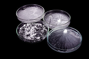
Crystallization or crystallisation is the process by which solid forms, where the atoms or molecules are highly organized into a structure known as a crystal. Some of the ways by which crystals form are precipitating from a solution, freezing, or more rarely deposition directly from a gas. Attributes of the resulting crystal depend largely on factors such as temperature, air pressure, and in the case of liquid crystals, time of fluid evaporation.

Crystallization occurs in two major steps. The first is nucleation, the appearance of a crystalline phase from either a supercooled liquid or a supersaturated solvent. The second step is known as crystal growth, which is the increase in the size of particles and leads to a crystal state. An important feature of this step is that loose particles form layers at the crystal's surface and lodge themselves into open inconsistencies such as pores, cracks, etc.

The majority of minerals and organic molecules crystallize easily, and the resulting crystals are generally of good quality, i.e. without visible defects. However, larger biochemical particles, like proteins, are often difficult to crystallize. The ease with which molecules will crystallize strongly depends on the intensity of either atomic forces (in the case of mineral substances), intermolecular forces (organic and biochemical substances) or intramolecular forces (biochemical substances).

Crystallization is also a chemical solid–liquid separation technique, in which mass transfer of a solute from the liquid solution to a pure solid crystalline phase occurs. In chemical engineering, crystallization occurs in a crystallizer. Crystallization is therefore related to precipitation, although the result is not amorphous or disordered, but a crystal.

Process

The crystallization process consists of two major events, nucleation and crystal growth which are driven by thermodynamic properties as well as chemical properties. In crystallization nucleation is the step where the solute molecules or atoms dispersed in the solvent start to gather into clusters, on the microscopic scale (elevating solute concentration in a small region), that become stable under the current operating conditions. These stable clusters constitute the nuclei. Therefore, the clusters need to reach a critical size in order to become stable nuclei. Such critical size is dictated by many different factors (temperature, supersaturation, etc.). It is at the stage of nucleation that the atoms or molecules arrange in a defined and periodic manner that defines the crystal structure – note that "crystal structure" is a special term that refers to the relative arrangement of the atoms or molecules, not the macroscopic properties of the crystal (size and shape), although those are a result of the internal crystal structure.

The crystal growth is the subsequent size increase of the nuclei that succeed in achieving the critical cluster size. Crystal growth is a dynamic process occurring in equilibrium where solute molecules or atoms precipitate out of solution, and dissolve back into solution. Supersaturation is one of the driving forces of crystallization, as the solubility of a species is an equilibrium process quantified by Ksp. Depending upon the conditions, either nucleation or growth may be predominant over the other, dictating crystal size.

Many compounds have the ability to crystallize with some having different crystal structures, a phenomenon called polymorphism. Certain polymorphs may be metastable, meaning that although it is not in thermodynamic equilibrium, it is kinetically stable and requires some input of energy to initiate a transformation to the equilibrium phase. Each polymorph is in fact a different thermodynamic solid state and crystal polymorphs of the same compound exhibit different physical properties, such as dissolution rate, shape (angles between facets and facet growth rates), melting point, etc. For this reason, polymorphism is of major importance in industrial manufacture of crystalline products. Additionally, crystal phases can sometimes be interconverted by varying factors such as temperature, such as in the transformation of anatase to rutile phases of titanium dioxide.

In nature

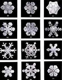
Snowflakes are a very well-known example, where subtle differences in crystal growth conditions result in different geometries.
 
Crystallized honey

There are many examples of natural process that involve crystallization.

Geological time scale process examples include:

Human time scale process examples include:

  • Snow flakes formation;
  • Honey crystallization (nearly all types of honey crystallize).

Methods

Crystal formation can be divided into two types, where the first type of crystals are composed of a cation and anion, also known as a salt, such as sodium acetate. The second type of crystals are composed of uncharged species, for example menthol.

Crystal formation can be achieved by various methods, such as: cooling, evaporation, addition of a second solvent to reduce the solubility of the solute (technique known as antisolvent or drown-out), solvent layering, sublimation, changing the cation or anion, as well as other methods.

The formation of a supersaturated solution does not guarantee crystal formation, and often a seed crystal or scratching the glass is required to form nucleation sites.

A typical laboratory technique for crystal formation is to dissolve the solid in a solution in which it is partially soluble, usually at high temperatures to obtain supersaturation. The hot mixture is then filtered to remove any insoluble impurities. The filtrate is allowed to slowly cool. Crystals that form are then filtered and washed with a solvent in which they are not soluble, but is miscible with the mother liquor. The process is then repeated to increase the purity in a technique known as recrystallization.

For biological molecules in which the solvent channels continue to be present to retain the three dimensional structure intact, microbatch crystallization under oil and vapor diffusion methods have been the common methods.

Typical equipment

Equipment for the main industrial processes for crystallization.

  1. Tank crystallizers. Tank crystallization is an old method still used in some specialized cases. Saturated solutions, in tank crystallization, are allowed to cool in open tanks. After a period of time the mother liquor is drained and the crystals removed. Nucleation and size of crystals are difficult to control. Typically, labor costs are very high.

Thermodynamic view

Low-temperature SEM magnification series for a snow crystal. The crystals are captured, stored, and sputter-coated with platinum at cryo-temperatures for imaging.

The crystallization process appears to violate the second principle of thermodynamics. Whereas most processes that yield more orderly results are achieved by applying heat, crystals usually form at lower temperatures – especially by supercooling. However, due to the release of the heat of fusion during crystallization, the entropy of the universe increases, thus this principle remains unaltered.

The molecules within a pure, perfect crystal, when heated by an external source, will become liquid. This occurs at a sharply defined temperature (different for each type of crystal). As it liquifies, the complicated architecture of the crystal collapses. Melting occurs because the entropy (S) gain in the system by spatial randomization of the molecules has overcome the enthalpy (H) loss due to breaking the crystal packing forces:

Regarding crystals, there are no exceptions to this rule. Similarly, when the molten crystal is cooled, the molecules will return to their crystalline form once the temperature falls beyond the turning point. This is because the thermal randomization of the surroundings compensates for the loss of entropy that results from the reordering of molecules within the system. Such liquids that crystallize on cooling are the exception rather than the rule.

The nature of a crystallization process is governed by both thermodynamic and kinetic factors, which can make it highly variable and difficult to control. Factors such as impurity level, mixing regime, vessel design, and cooling profile can have a major impact on the size, number, and shape of crystals produced.

Dynamics

As mentioned above, a crystal is formed following a well-defined pattern, or structure, dictated by forces acting at the molecular level. As a consequence, during its formation process the crystal is in an environment where the solute concentration reaches a certain critical value, before changing status. Solid formation, impossible below the solubility threshold at the given temperature and pressure conditions, may then take place at a concentration higher than the theoretical solubility level. The difference between the actual value of the solute concentration at the crystallization limit and the theoretical (static) solubility threshold is called supersaturation and is a fundamental factor in crystallization.

Nucleation

Nucleation is the initiation of a phase change in a small region, such as the formation of a solid crystal from a liquid solution. It is a consequence of rapid local fluctuations on a molecular scale in a homogeneous phase that is in a state of metastable equilibrium. Total nucleation is the sum effect of two categories of nucleation – primary and secondary.

Primary nucleation

Primary nucleation is the initial formation of a crystal where there are no other crystals present or where, if there are crystals present in the system, they do not have any influence on the process. This can occur in two conditions. The first is homogeneous nucleation, which is nucleation that is not influenced in any way by solids. These solids include the walls of the crystallizer vessel and particles of any foreign substance. The second category, then, is heterogeneous nucleation. This occurs when solid particles of foreign substances cause an increase in the rate of nucleation that would otherwise not be seen without the existence of these foreign particles. Homogeneous nucleation rarely occurs in practice due to the high energy necessary to begin nucleation without a solid surface to catalyse the nucleation.

Primary nucleation (both homogeneous and heterogeneous) has been modelled with the following:

where

B is the number of nuclei formed per unit volume per unit time,
N is the number of nuclei per unit volume,
kn is a rate constant,
c is the instantaneous solute concentration,
c* is the solute concentration at saturation,
(cc*) is also known as supersaturation,
n is an empirical exponent that can be as large as 10, but generally ranges between 3 and 4.

Secondary nucleation

Secondary nucleation is the formation of nuclei attributable to the influence of the existing microscopic crystals in the magma. Simply put, secondary nucleation is when crystal growth is initiated with contact of other existing crystals or "seeds". The first type of known secondary crystallization is attributable to fluid shear, the other due to collisions between already existing crystals with either a solid surface of the crystallizer or with other crystals themselves. Fluid-shear nucleation occurs when liquid travels across a crystal at a high speed, sweeping away nuclei that would otherwise be incorporated into a crystal, causing the swept-away nuclei to become new crystals. Contact nucleation has been found to be the most effective and common method for nucleation. The benefits include the following:

  • Low kinetic order and rate-proportional to supersaturation, allowing easy control without unstable operation.
  • Occurs at low supersaturation, where growth rate is optimal for good quality.
  • Low necessary energy at which crystals strike avoids the breaking of existing crystals into new crystals.
  • The quantitative fundamentals have already been isolated and are being incorporated into practice.

The following model, although somewhat simplified, is often used to model secondary nucleation:

where

k1 is a rate constant,
MT is the suspension density,
j is an empirical exponent that can range up to 1.5, but is generally 1,
b is an empirical exponent that can range up to 5, but is generally 2.
Crystal growth

Growth

Once the first small crystal, the nucleus, forms it acts as a convergence point (if unstable due to supersaturation) for molecules of solute touching – or adjacent to – the crystal so that it increases its own dimension in successive layers. The pattern of growth resembles the rings of an onion, as shown in the picture, where each colour indicates the same mass of solute; this mass creates increasingly thin layers due to the increasing surface area of the growing crystal. The supersaturated solute mass the original nucleus may capture in a time unit is called the growth rate expressed in kg/(m2*h), and is a constant specific to the process. Growth rate is influenced by several physical factors, such as surface tension of solution, pressure, temperature, relative crystal velocity in the solution, Reynolds number, and so forth.

The main values to control are therefore:

  • Supersaturation value, as an index of the quantity of solute available for the growth of the crystal;
  • Total crystal surface in unit fluid mass, as an index of the capability of the solute to fix onto the crystal;
  • Retention time, as an index of the probability of a molecule of solute to come into contact with an existing crystal;
  • Flow pattern, again as an index of the probability of a molecule of solute to come into contact with an existing crystal (higher in laminar flow, lower in turbulent flow, but the reverse applies to the probability of contact).

The first value is a consequence of the physical characteristics of the solution, while the others define a difference between a well- and poorly designed crystallizer.

Size distribution

The appearance and size range of a crystalline product is extremely important in crystallization. If further processing of the crystals is desired, large crystals with uniform size are important for washing, filtering, transportation, and storage, because large crystals are easier to filter out of a solution than small crystals. Also, larger crystals have a smaller surface area to volume ratio, leading to a higher purity. This higher purity is due to less retention of mother liquor which contains impurities, and a smaller loss of yield when the crystals are washed to remove the mother liquor. In special cases, for example during drug manufacturing in the pharmaceutical industry, small crystal sizes are often desired to improve drug dissolution rate and bio-availability. The theoretical crystal size distribution can be estimated as a function of operating conditions with a fairly complicated mathematical process called population balance theory (using population balance equations).

Main crystallization processes

Crystallization of sodium acetate.

Some of the important factors influencing solubility are:

  • Concentration
  • Temperature
  • Solvent mixture composition
  • Polarity
  • Ionic strength

So one may identify two main families of crystallization processes:

  • Cooling crystallization
  • Evaporative crystallization

This division is not really clear-cut, since hybrid systems exist, where cooling is performed through evaporation, thus obtaining at the same time a concentration of the solution.

A crystallization process often referred to in chemical engineering is the fractional crystallization. This is not a different process, rather a special application of one (or both) of the above.

Cooling crystallization

Application

Most chemical compounds, dissolved in most solvents, show the so-called direct solubility that is, the solubility threshold increases with temperature.

Solubility of the system Na2SO4 – H2O

So, whenever the conditions are favorable, crystal formation results from simply cooling the solution. Here cooling is a relative term: austenite crystals in a steel form well above 1000 °C. An example of this crystallization process is the production of Glauber's salt, a crystalline form of sodium sulfate. In the diagram, where equilibrium temperature is on the x-axis and equilibrium concentration (as mass percent of solute in saturated solution) in y-axis, it is clear that sulfate solubility quickly decreases below 32.5 °C. Assuming a saturated solution at 30 °C, by cooling it to 0 °C (note that this is possible thanks to the freezing-point depression), the precipitation of a mass of sulfate occurs corresponding to the change in solubility from 29% (equilibrium value at 30 °C) to approximately 4.5% (at 0 °C) – actually a larger crystal mass is precipitated, since sulfate entrains hydration water, and this has the side effect of increasing the final concentration.

There are limitations in the use of cooling crystallization:

  • Many solutes precipitate in hydrate form at low temperatures: in the previous example this is acceptable, and even useful, but it may be detrimental when, for example, the mass of water of hydration to reach a stable hydrate crystallization form is more than the available water: a single block of hydrate solute will be formed – this occurs in the case of calcium chloride);
  • Maximum supersaturation will take place in the coldest points. These may be the heat exchanger tubes which are sensitive to scaling, and heat exchange may be greatly reduced or discontinued;
  • A decrease in temperature usually implies an increase of the viscosity of a solution. Too high a viscosity may give hydraulic problems, and the laminar flow thus created may affect the crystallization dynamics.
  • It is not applicable to compounds having reverse solubility, a term to indicate that solubility increases with temperature decrease (an example occurs with sodium sulfate where solubility is reversed above 32.5 °C).

Cooling crystallizers

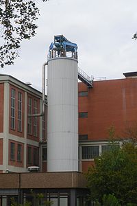
Vertical cooling crystallizer in a beet sugar factory

The simplest cooling crystallizers are tanks provided with a mixer for internal circulation, where temperature decrease is obtained by heat exchange with an intermediate fluid circulating in a jacket. These simple machines are used in batch processes, as in processing of pharmaceuticals and are prone to scaling. Batch processes normally provide a relatively variable quality of the product along with the batch.

The Swenson-Walker crystallizer is a model, specifically conceived by Swenson Co. around 1920, having a semicylindric horizontal hollow trough in which a hollow screw conveyor or some hollow discs, in which a refrigerating fluid is circulated, plunge during rotation on a longitudinal axis. The refrigerating fluid is sometimes also circulated in a jacket around the trough. Crystals precipitate on the cold surfaces of the screw/discs, from which they are removed by scrapers and settle on the bottom of the trough. The screw, if provided, pushes the slurry towards a discharge port.

A common practice is to cool the solutions by flash evaporation: when a liquid at a given T0 temperature is transferred in a chamber at a pressure P1 such that the liquid saturation temperature T1 at P1 is lower than T0, the liquid will release heat according to the temperature difference and a quantity of solvent, whose total latent heat of vaporization equals the difference in enthalpy. In simple words, the liquid is cooled by evaporating a part of it.

In the sugar industry, vertical cooling crystallizers are used to exhaust the molasses in the last crystallization stage downstream of vacuum pans, prior to centrifugation. The massecuite enters the crystallizers at the top, and cooling water is pumped through pipes in counterflow.

Evaporative crystallization

Another option is to obtain, at an approximately constant temperature, the precipitation of the crystals by increasing the solute concentration above the solubility threshold. To obtain this, the solute/solvent mass ratio is increased using the technique of evaporation. This process is insensitive to change in temperature (as long as hydration state remains unchanged).

All considerations on control of crystallization parameters are the same as for the cooling models.

Evaporative crystallizers

Most industrial crystallizers are of the evaporative type, such as the very large sodium chloride and sucrose units, whose production accounts for more than 50% of the total world production of crystals. The most common type is the forced circulation (FC) model (see evaporator). A pumping device (a pump or an axial flow mixer) keeps the crystal slurry in homogeneous suspension throughout the tank, including the exchange surfaces; by controlling pump flow, control of the contact time of the crystal mass with the supersaturated solution is achieved, together with reasonable velocities at the exchange surfaces. The Oslo, mentioned above, is a refining of the evaporative forced circulation crystallizer, now equipped with a large crystals settling zone to increase the retention time (usually low in the FC) and to roughly separate heavy slurry zones from clear liquid. Evaporative crystallizers tend to yield larger average crystal size and narrows the crystal size distribution curve.

DTB crystallizer

DTB Crystallizer
 
Schematic of DTB

Whichever the form of the crystallizer, to achieve an effective process control it is important to control the retention time and the crystal mass, to obtain the optimum conditions in terms of crystal specific surface and the fastest possible growth. This is achieved by a separation – to put it simply – of the crystals from the liquid mass, in order to manage the two flows in a different way. The practical way is to perform a gravity settling to be able to extract (and possibly recycle separately) the (almost) clear liquid, while managing the mass flow around the crystallizer to obtain a precise slurry density elsewhere. A typical example is the DTB (Draft Tube and Baffle) crystallizer, an idea of Richard Chisum Bennett (a Swenson engineer and later President of Swenson) at the end of the 1950s. The DTB crystallizer (see images) has an internal circulator, typically an axial flow mixer – yellow – pushing upwards in a draft tube while outside the crystallizer there is a settling area in an annulus; in it the exhaust solution moves upwards at a very low velocity, so that large crystals settle – and return to the main circulation – while only the fines, below a given grain size are extracted and eventually destroyed by increasing or decreasing temperature, thus creating additional supersaturation. A quasi-perfect control of all parameters is achieved as DTF crystallizers offer superior control over crystal size and characteristics. This crystallizer, and the derivative models (Krystal, CSC, etc.) could be the ultimate solution if not for a major limitation in the evaporative capacity, due to the limited diameter of the vapour head and the relatively low external circulation not allowing large amounts of energy to be supplied to the system.
Polymorphism (materials science)

In materials science, polymorphism describes the existence of a solid material in more than one form or crystal structure. Polymorphism is a form of isomerism. Any crystalline material can exhibit the phenomenon. Allotropy refers to polymorphism for chemical elements. Polymorphism is of practical relevance to pharmaceuticals, agrochemicals, pigments, dyestuffs, foods, and explosives. According to IUPAC, a polymorphic transition is "A reversible transition of a solid crystalline phase at a certain temperature and pressure (the inversion point) to another phase of the same chemical composition with a different crystal structure." According to McCrone, polymorphs are "different in crystal structure but identical in the liquid or vapor states." Materials with two polymorphs are called dimorphic, with three polymorphs, trimorphic, etc.

Examples

Many compounds exhibit polymorphism. It has been claimed that "every compound has different polymorphic forms, and that, in general, the number of forms known for a given compound is proportional to the time and money spent in research on that compound."

Organic compounds

Calcite (top) and Aragonite (bottom), two forms of calcium carbonate. Note: the colors are from impurities.

Benzamide

The phenomenon was discovered in 1832 by Friedrich Wöhler and Justus von Liebig. They observed that the silky needles of freshly crystallized benzamide slowly converted to rhombic crystals. Present-day analysis identifies three polymorphs for benzamide: the least stable one, formed by flash cooling is the orthorhombic form II. This type is followed by the monoclinic form III (observed by Wöhler/Liebig). The most stable form is monoclinic form I. The hydrogen bonding mechanisms are the same for all three phases; however, they differ strongly in their pi-pi interactions.

Maleic acid

In 2006 a new polymorph of maleic acid was discovered, fully 124 years after the first crystal form was studied. Maleic acid is manufactured on an industrial scale in the chemical industry. It forms salt found in medicine. The new crystal type is produced when a co-crystal of caffeine and maleic acid (2:1) is dissolved in chloroform and when the solvent is allowed to evaporate slowly. Whereas form I has monoclinic space group P21/c, the new form has space group Pc. Both polymorphs consist of sheets of molecules connected through hydrogen bonding of the carboxylic acid groups; but, in form I, the sheets alternate with respect of the net dipole moment, whereas, in form II, the sheets are oriented in the same direction.

1,3,5-Trinitrobenzene

After 125 years of study, 1,3,5-trinitrobenzene yielded a second polymorph. The usual form has the space group Pbca, but in 2004, a second polymorph was obtained in the space group Pca21 when the compound was crystallised in the presence of an additive, trisindane. This experiment shows that additives can induce the appearance of polymorphic forms.

Other organic compounds

Acridine has been obtained as eight polymorphs and aripiprazole has nine. The record for the largest number of well-characterised polymorphs is held by a compound known as ROY. Glycine crystallizes as both monoclinic and hexagonal crystals. Polymorphism in organic compounds is often the result of conformational polymorphism.

Inorganic compounds

Binary metal oxides

Polymorphism in binary metal oxides has attracted much attention because these materials are of significant economic value. One set of famous examples have the composition SiO2, which form many polymorphs. Important ones include: α-quartz, β-quartz, tridymite, cristobalite, moganite, coesite, and stishovite.

Metal oxides Phase Conditions of P and T Structure/Space Group
CrO2 α phase Ambient conditions Rutile-type Tetragonal (P42/mnm)
β phase RT and 14 GPa CaCl2-type Orthorhombic
RT and 12±3 GPa
Cr2O3 Corundum phase Ambient conditions Corundum-type Rhombohedral (R3c)
High pressure phase RT and 35 GPa Rh2O3-II type
Fe2O3 α phase Ambient conditions Corundum-type Rhombohedral (R3c)
β phase Below 773 K Body-centered cubic (Ia3)
γ phase Up to 933 K Cubic spinel structure (Fd3m)
ε phase -- Rhombic (Pna21)
Bi2O3 α phase Ambient conditions Monoclinic (P21/c)
β phase 603-923 K and 1 atm Tetragonal
γ phase 773-912 K or RT and 1 atm Body-centered cubic
δ phase 912-1097 K and 1 atm FCC (Fm3m)
In2O3 Bixbyite-type phase Ambient conditions Cubic (Ia3)
Corundum-type 15-25 GPa at 1273 K Corundum-type Hexagonal (R3c)
Rh2O3(II)-type 100 GPa and 1000 K Orthorhombic
Al2O3 α phase Ambient conditions Corundum-type Trigonal (R3c)
γ phase 773 K and 1 atm Cubic (Fd3m)
SnO2 α phase Ambient conditions Rutile-type Tetragonal (P42/mnm)
CaCl2-type phase 15 KBar at 1073 K Orthorhombic, CaCl2-type (Pnnm)
α-PbO2-type Above 18 KBar α-PbO2-type (Pbcn)
TiO2 Rutile Equilibrium phase Rutile-type Tetragonal
Anatase Metastable phase (Not stable) Tetragonal (I41/amd)
Brookite Metastable phase (Not stable) Orthorhombic (Pcab)
ZrO2 Monoclinic phase Ambient conditions Monoclinic (P21/c)
Tetragonal phase Above 1443 K Tetragonal (P42/nmc)
Fluorite-type phase Above 2643 K Cubic (Fm3m)
MoO3 α phase 553-673 K & 1 atm Orthorhombic (Pbnm)
β phase 553-673 K & 1 atm Monoclinic
h phase High-pressure and high-temperature phase Hexagonal (P6a/m or P6a)
MoO3-II 60 kbar and 973 K Monoclinic
WO3 ε phase Up to 220 K Monoclinic (Pc)
δ phase 220-300 K Triclinic (P1)
γ phase 300-623 K Monoclinic (P21/n)
β phase 623-900 K Orthorhombic (Pnma)
α phase Above 900 K Tetragonal (P4/ncc)

Other inorganic materials

Classical examples of polymorphism are the pair of minerals calcite and aragonite, both forms of calcium carbonate. Perhaps the most famous example is that of the polymorphs of carbon: graphite and diamond.

β-HgS precipitates as a black solid when Hg(II) salts are treated with H2S. With gentle heating of the slurry, the black polymorph converts to the red form.

Factors affecting polymorphism

According to Ostwald's rule, usually less stable polymorphs crystallize before the stable form. The concept hinges on the idea that unstable polymorphs more closely resemble the state in solution, and thus are kinetically advantaged. The founding case of fibrous vs rhombic benzamide illustrates the case. Another example is provided by two polymorphs of titanium dioxide.

Polymorphs have disparate stabilities. Some convert rapidly at room (or any) temperature. Most polymorphs of organic molecules only differ by a few kJ/mol in lattice energy. Approximately 50% of known polymorph pairs differ by less than 2 kJ/mol and stability differences of more than 10 kJ/mol are rare.

Polymorphism is affected by the details of crystallisation. The solvent in all respects affects the nature of the polymorph, including concentration, other components of the solvent, i.e., species that inhibiting or promote certain growth patterns. A decisive factor is often the temperature of the solvent from which crystallisation is carried out.

Metastable polymorphs are not always reproducibly obtained, leading to cases of "disappearing polymorphs".

In pharmaceuticals

Drugs receive regulatory approval for only a single polymorph. In a classic patent dispute, the GlaxoSmithKline defended its patent for the polymorph type II of the active ingredient in Zantac against competitors while that of the polymorph type I had already expired. Polymorphism in drugs can also have direct medical implications since dissolution rates depend on the polymorph. Polymorphic purity of drug samples can be checked using techniques such as powder X-ray diffraction, IR/Raman spectroscopy, and utilizing the differences in their optical properties in some cases.

Case studies

Ritonavir

The antiviral drug ritonavir exists as two polymorphs, which differ greatly in efficacy. Such issues were solved by reformulating the medicine into gelcaps and tablets, rather than the original capsules.

Acetylsalicylic acid

A second polymorph of acetylsalicylic acid was reported only in 2005. A new crystal type was found after attempted co-crystallization of aspirin and levetiracetam from hot acetonitrile. In form I, pairs of aspirin molecules form centrosymmetric dimers through the acetyl groups with the (acidic) methyl proton to carbonyl hydrogen bonds. In form II, each aspirin molecule forms the same hydrogen bonds, but with two neighbouring molecules instead of one. With respect to the hydrogen bonds formed by the carboxylic acid groups, both polymorphs form identical dimer structures. The aspirin polymorphs contain identical 2-dimensional sections and are therefore more precisely described as polytypes.

Paracetamol

Paracetamol powder has poor compression properties, which poses difficulty in making tablets. A second polymorph was found with more suitable compressive properties.

Cortisone acetate

Cortisone acetate exists in at least five different polymorphs, four of which are unstable in water and change to a stable form.

Carbamazepine

Carbamazepine, estrogen, paroxetine, and chloramphenicol also show polymorphism.

Polytypism

Polytypes are a special case of polymorphs, where multiple close-packed crystal structures differ in one dimension only. Polytypes have identical close-packed planes, but differ in the stacking sequence in the third dimension perpendicular to these planes. Silicon carbide (SiC) has more than 170 known polytypes, although most are rare. All the polytypes of SiC have virtually the same density and Gibbs free energy. The most common SiC polytypes are shown in Table 1.

Table 1: Some polytypes of SiC.

Phase Structure Ramsdell notation Stacking sequence Comment
α-SiC hexagonal 2H AB wurtzite form
α-SiC hexagonal 4H ABCB
α-SiC hexagonal 6H ABCACB the most stable and common form
α-SiC rhombohedral 15R ABCACBCABACABCB
β-SiC face-centered cubic 3C ABC sphalerite or zinc blende form

A second group of materials with different polytypes are the transition metal dichalcogenides, layered materials such as molybdenum disulfide (MoS2). For these materials the polytypes have more distinct effects on material properties, e.g. for MoS2, the 1T polytype is metallic in character, while the 2H form is more semiconducting. Another example is tantalum disulfide, where the common 1T as well as 2H polytypes occur, but also more complex 'mixed coordination' types such as 4Hb and 6R, where the trigonal prismatic and the octahedral geometry layers are mixed. Here, the 1T polytype exhibits a charge density wave, with distinct influence on the conductivity as a function of temperature, while the 2H polytype exhibits superconductivity.

ZnS and CdI2 are also polytypical. It has been suggested that this type of polymorphism is due to kinetics where screw dislocations rapidly reproduce partly disordered sequences in a periodic fashion.

Theory

In terms of thermodynamics, two types of polymorphic behaviour are recognized. For a monotropic system, plots of the free energies of the various polymorphs against temperature do not cross before all polymorphs melt. As a result any transition from one polymorph to another below the melting point will be irreversible. For an enantiotropic system, a plot of the free energy against temperature shows a crossing point before the various melting points. It may also be possible to convert interchangeably between the two polymorphs by heating or cooling, or through physical contact with a lower energy polymorph.

Solid phase transitions which transform reversibly without passing through the liquid or gaseous phases are called enantiotropic. In contrast, if the modifications are not convertible under these conditions, the system is monotropic. Experimental data are used to differentiate between enantiotropic and monotropic transitions and energy/temperature semi-quantitative diagrams can be drawn by applying several rules, principally the heat-of-transition rule, the heat-of-fusion rule and the density rule. These rules enable the deduction of the relative positions of the H and Gisobars in the E/T diagram.

Chemiresistor

From Wikipedia, the free encyclopedia
https://en.wikipedia.org/wiki/Chemiresistor

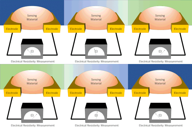
Simplified schematic of a single gap chemiresistive sensor. (not to scale)

A chemiresistor is a material that changes its electrical resistance in response to changes in the nearby chemical environment. Chemiresistors are a class of chemical sensors that rely on the direct chemical interaction between the sensing material and the analyte. The sensing material and the analyte can interact by covalent bonding, hydrogen bonding, or molecular recognition. Several different materials have chemiresistor properties: metal-oxide semiconductors, some conductive polymers, and nanomaterials like graphene, carbon nanotubes and nanoparticles. Typically these materials are used as partially selective sensors in devices like electronic tongues or electronic noses.

A basic chemiresistor consists of a sensing material that bridges the gap between two electrodes or coats a set of interdigitated electrodes. The resistance between the electrodes can be easily measured. The sensing material has an inherent resistance that can be modulated by the presence or absence of the analyte. During exposure, analytes interact with the sensing material. These interactions cause changes in the resistance reading. In some chemiresistors the resistance changes simply indicate the presence of analyte. In others, the resistance changes are proportional to the amount of analyte present; this allows for the amount of analyte present to be measured.

History

As far back as 1965 there are reports of semiconductor materials exhibiting electrical conductivities that are strongly affected by ambient gases and vapours. However, it was not until 1985 that Wohltjen and Snow coined the term chemiresistor. The chemiresistive material they investigated was copper phthalocyanine, and they demonstrated that its resistivity decreased in the presence of ammonia vapour at room temperature.

In recent years chemiresistor technology has been used to develop promising sensors for many applications, including conductive polymer sensors for secondhand smoke, carbon nanotube sensors for gaseous ammonia, and metal oxide sensors for hydrogen gas. The ability of chemiresistors to provide accurate real-time information about the environment through small devices that require minimal electricity makes them an appealing addition to the internet of things.

Types of chemiresistor sensors

An oxygen sensing TiO2 film on an interdigitated electrode.

Device architectures

Chemiresistors can be made by coating an interdigitated electrode with a thin film or by using a thin film or other sensing material to bridge the single gap between two electrodes. Electrodes are typically made of conductive metals such as gold and chromium which make good ohmic contact with thin films. In both architectures, the chemiresistant sensing material controls the conductance between the two electrodes; however, each device architecture has its own advantages and disadvantages.

Interdigitated electrodes allow for a greater amount of the film's surface area to be in contact with the electrode. This allows for more electrical connections to be made and increases the overall conductivity of the system. Interdigitated electrodes with finger sizes and finger spacing on the order of microns are difficult to manufacture and require the use of photolithography. Larger features are easier to fabricate and can be manufactured using techniques such as thermal evaporation. Both interdigitated electrode and single-gap systems can be arranged in parallel to allow for the detection of multiple analytes by one device.

Sensing materials

Metal oxide semiconductors

Metal oxide chemiresistor sensors were first commercialized in 1970 in a carbon monoxide detector that used powdered SnO2. However, there are many other metal oxides that have chemiresistive properties. Metal oxide sensors are primarily gas sensors, and they can sense both oxidizing and reducing gases. This makes them ideal for use in industrial situations where gases used in manufacturing can pose a risk to worker safety.

Sensors made from metal oxides require high temperatures (200 °C or higher) to operate because, in order for the resistivity to change, an activation energy must be overcome.

Metal oxide chemiresistors
Metal oxide Vapours
Chromium titanium oxide H2S
Gallium oxide O2, CO
Indium oxide O3
Molybdenum oxide NH3
Tin oxide reducing gases
Tungsten oxide NO2
Zinc oxide hydrocarbons, O2
A graphene monolayer.

Graphene

In comparison to the other materials graphene chemiresistor sensors are relatively new but have shown excellent sensitivity. Graphene is an allotrope of carbon that consists of a single layer of graphite. It has been used in sensors to detect vapour-phase molecules, pH, proteins, bacteria, and simulated chemical warfare agents.

Carbon nanotubes

The first published report of nanotubes being used as chemiresistors was made in 2000. Since then there has been research into chemiresistors and chemically sensitive field effect transistors fabricated from individual single-walled nanotubes, bundles of single-walled nanotubes, bundles of multi-walled nanotubes, and carbon nanotube–polymer mixtures. It has been shown that a chemical species can alter the resistance of a bundle of single-walled carbon nanotubes through multiple mechanisms.

Carbon nanotubes are useful sensing materials because they have low detection limits, and quick response times; however, bare carbon nanotube sensors are not very selective. They can respond to the presence of many different gases from gaseous ammonia to diesel fumes. Carbon nanotube sensors can be made more selective by using a polymer as a barrier, doping the nanotubes with heteroatoms, or adding functional groups to the surface of the nanotubes.

Circular interdigitated electrodes with and without a gold nanoparticle chemiresistor film

.

Nanoparticles

Many different nanoparticles of varying size, structure and composition have been incorporated into chemiresistor sensors. The most commonly used are thin films of gold nanoparticles coated with self-assembled monolayers (SAMs) of organic molecules. The SAM is critical in defining some of the nanoparticle assembly’s properties. Firstly, the stability of the gold nanoparticles depends upon the integrity of the SAM, which prevents them from sintering together. Secondly, the SAM of organic molecules defines the separation between the nanoparticles, e.g. longer molecules cause the nanoparticles to have a wider average separation. The width of this separation defines the barrier that electrons must tunnel through when a voltage is applied and electric current flows. Thus by defining the average distance between individual nanoparticles the SAM also defines the electrical resistivity of the nanoparticle assembly. Finally, the SAMs form a matrix around the nanoparticles that chemical species can diffuse into. As new chemical species enter the matrix it changes the inter-particle separation which in turn affects the electrical resistance. Analytes diffuse into the SAMs at proportions defined by their partition coefficient and this characterizes the selectivity and sensitivity of the chemiresistor material.

Polymerization of a polymer around a target molecule that is then washed out to leave shaped cavities behind.

Conductive polymers

Conductive polymers such as polyaniline and polypyrrole can be used as sensing materials when the target interacts directly with the polymer chain resulting in a change in conductivity of the polymer. These types of systems lack selectivity due to the wide range of target molecules that can interact with the polymer. Molecularly imprinted polymers can add selectivity to conductive polymer chemiresistors. A molecularly imprinted polymer is made by polymerizing a polymer around a target molecule and then removing the target molecule from the polymer leaving behind cavities matching the size and shape of the target molecule. Molecularly imprinting the conductive polymer increases the sensitivity of the chemiresistor by selecting for the target's general size and shape as well as its ability to interact with the chain of the conductive polymer.

Band gap

From Wikipedia, the free encyclopedia
https://en.wikipedia.org/wiki/Band_gap

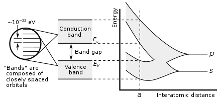
Showing how electronic band structure comes about in the hypothetical example of a large number of carbon atoms being brought together to form a diamond crystal. The graph (right) shows the energy levels as a function of the spacing between atoms. When the atoms are far apart (right side of graph) each atom has valence atomic orbitals p and s which have the same energy. However when the atoms come closer together their orbitals begin to overlap. Due to Bloch's theorem which describes the hybridization of the orbitals of the N atoms in the crystal, the N atomic orbitals of equal energy split into N molecular orbitals each with a different energy. Since N is such a large number, adjacent orbitals are extremely close together in energy so the orbitals can be considered a continuous energy band. a is the atomic spacing in an actual crystal of diamond. At that spacing the orbitals form two bands, called the valence and conduction bands, with a 5.5 eV band gap between them. At room temperature, very few electrons have the thermal energy to surmount this wide energy gap and become conduction electrons, so diamond is an insulator. An analogous treatment of silicon with the same crystal structure yields a much smaller band gap of 1.1 eV making silicon a semiconductor.

In solid-state physics, a band gap, also called an energy gap, is an energy range in a solid where no electronic states can exist. In graphs of the electronic band structure of solids, the band gap generally refers to the energy difference (in electron volts) between the top of the valence band and the bottom of the conduction band in insulators and semiconductors. It is the energy required to promote a valence electron bound to an atom to become a conduction electron, which is free to move within the crystal lattice and serve as a charge carrier to conduct electric current. It is closely related to the HOMO/LUMO gap in chemistry. If the valence band is completely full and the conduction band is completely empty, then electrons cannot move within the solid because there are no available states. If the electrons are not free to move within the crystal lattice, then there is no generated current due to no net charge carrier mobility. However, if some electrons transfer from the valence band (mostly full) to the conduction band (mostly empty), then current can flow (see carrier generation and recombination). Therefore, the band gap is a major factor determining the electrical conductivity of a solid. Substances with large band gaps are generally insulators, those with smaller band gaps are semiconductors, while conductors either have very small band gaps or none, because the valence and conduction bands overlap to form a continuous band.

In semiconductor physics

Semiconductor band structure.

Every solid has its own characteristic energy-band structure. This variation in band structure is responsible for the wide range of electrical characteristics observed in various materials. Depending on the dimension, the band structure and spectroscopy can vary. The different types of dimensions are as listed: one dimension, two dimensions, and three dimensions.

In semiconductors and insulators, electrons are confined to a number of bands of energy, and forbidden from other regions because there are no allowable electronic states for them to occupy. The term "band gap" refers to the energy difference between the top of the valence band and the bottom of the conduction band. Electrons are able to jump from one band to another. However, in order for a valence band electron to be promoted to the conduction band, it requires a specific minimum amount of energy for the transition. This required energy is an intrinsic characteristic of the solid material. Electrons can gain enough energy to jump to the conduction band by absorbing either a phonon (heat) or a photon (light).

A semiconductor is a material with an intermediate-sized, non-zero band gap that behaves as an insulator at T=0K, but allows thermal excitation of electrons into its conduction band at temperatures that are below its melting point. In contrast, a material with a large band gap is an insulator. In conductors, the valence and conduction bands may overlap, so there is no longer a bandgap with forbidden regions of electronic states.

The conductivity of intrinsic semiconductors is strongly dependent on the band gap. The only available charge carriers for conduction are the electrons that have enough thermal energy to be excited across the band gap and the electron holes that are left off when such an excitation occurs.

Band-gap engineering is the process of controlling or altering the band gap of a material by controlling the composition of certain semiconductor alloys, such as GaAlAs, InGaAs, and InAlAs. It is also possible to construct layered materials with alternating compositions by techniques like molecular-beam epitaxy. These methods are exploited in the design of heterojunction bipolar transistors (HBTs), laser diodes and solar cells.

The distinction between semiconductors and insulators is a matter of convention. One approach is to think of semiconductors as a type of insulator with a narrow band gap. Insulators with a larger band gap, usually greater than 4 eV, are not considered semiconductors and generally do not exhibit semiconductive behaviour under practical conditions. Electron mobility also plays a role in determining a material's informal classification.

The band-gap energy of semiconductors tends to decrease with increasing temperature. When temperature increases, the amplitude of atomic vibrations increase, leading to larger interatomic spacing. The interaction between the lattice phonons and the free electrons and holes will also affect the band gap to a smaller extent. The relationship between band gap energy and temperature can be described by Varshni's empirical expression (named after Y. P. Varshni),

, where Eg(0), α and β are material constants.

Furthermore, lattice vibrations increase with increasing temperature, which increases the effect of electron scattering. Additionally, the number of charge carriers within a semi-conductor will increase, as more carriers have the energy required to cross the band-gap threshold and so conductivity of semi-conductors also increases with increasing temperature.

In a regular semiconductor crystal, the band gap is fixed owing to continuous energy states. In a quantum dot crystal, the band gap is size dependent and can be altered to produce a range of energies between the valence band and conduction band. It is also known as quantum confinement effect.

Band gaps also depend on pressure. Band gaps can be either direct or indirect, depending on the electronic band structure of the material.

It was mentioned earlier that the dimensions have different band structure and spectroscopy. For non-metallic solids, which are one dimensional, have optical properties that are dependent on the electronic transitions between valence and conduction bands. In addition, the spectroscopic transition probability is between the initial and final orbital and it depends on the integral. φi is the initial orbital, φf is the final orbital, ʃ φf*ûεφi is the integral, ε is the electric vector, and u is the dipole moment.

Two-dimensional structures of solids behave because of the overlap of atomic orbitals. The simplest two-dimensional crystal contains identical atoms arranged on a square lattice. Energy splitting occurs at the Brillouin zone edge for one-dimensional situations because of a weak periodic potential, which produces a gap between bands. The behavior of the one-dimensional situations does not occur for two-dimensional cases because there are extra freedoms of motion. Furthermore, a bandgap can be produced with strong periodic potential for two-dimensional and three-dimensional cases.

Direct and indirect band gap

Based on the their band structure, materials are characterised with a direct band gap or indirect band gap. In the free-electron model, k is the momentum of a free electron and assumes unique values within the Brillouin zone that outlines the periodicity of the crystal lattice. If the momentum of the lowest energy state in the conduction band and the highest energy state of the valence band of a material have the same value, then the material has a direct bandgap. If they are not the same, then the material has an indirect band gap and the electronic transition must undergo momentum transfer to satisfy conservation. Such indirect "forbidden" transitions still occur, however at very low probabilities and weaker energy. For materials with a direct band gap, valence electrons can be directly excited into the conduction band by a photon whose energy is larger than the bandgap. In contrast, for materials with an indirect band gap, a photon and phonon must both be involved in a transition from the valence band top to the conduction band bottom, involving a momentum change. Therefore, direct bandgap materials tend to have stronger light emission and absorption properties and tend to be better suited for photovoltaics (PVs), light-emitting diodes (LEDs), and laser diodes; however, indirect bandgap materials are frequently used in PVs and LEDs when the materials have other favorable properties.

Light-emitting diodes and laser diodes

LEDs and laser diodes usually emit photons with energy close to and slightly larger than the band gap of the semiconductor material from which they are made. Therefore, as the band gap energy increases, the LED or laser color changes from infrared to red, through the rainbow to violet, then to UV.

Photovoltaic cells

The Shockley–Queisser limit gives the maximum possible efficiency of a single-junction solar cell under un-concentrated sunlight, as a function of the semiconductor band gap. If the band gap is too high, most daylight photons cannot be absorbed; if it is too low, then most photons have much more energy than necessary to excite electrons across the band gap, and the rest is wasted. The semiconductors commonly used in commercial solar cells have band gaps near the peak of this curve, for example silicon (1.1eV) or CdTe (1.5eV). The Shockley–Queisser limit has been exceeded experimentally by combining materials with different band gap energies to make tandem solar cells.

The optical band gap (see below) determines what portion of the solar spectrum a photovoltaic cell absorbs. A semiconductor will not absorb photons of energy less than the band gap; and the energy of the electron-hole pair produced by a photon is equal to the bandgap energy. A luminescent solar converter uses a luminescent medium to downconvert photons with energies above the band gap to photon energies closer to the band gap of the semiconductor comprising the solar cell.

List of band gaps

Below are band gap values for some selected materials. For a comprehensive list of band gaps in semiconductors, see List of semiconductor materials.

Group Material Symbol Band gap (eV) @ 302K
III–V Aluminium nitride AlN 6.0
IV Diamond C 5.5
IV Silicon Si 1.14
IV Germanium Ge 0.67
III–V Gallium nitride GaN 3.4
III–V Gallium phosphide GaP 2.26
III–V Gallium arsenide GaAs 1.43
IV–V Silicon nitride Si3N4 5
IV–VI Lead(II) sulfide PbS 0.37
IV–VI Silicon dioxide SiO2 9

Copper(I) oxide Cu2O 2.1

Optical versus electronic bandgap

In materials with a large exciton binding energy, it is possible for a photon to have just barely enough energy to create an exciton (bound electron–hole pair), but not enough energy to separate the electron and hole (which are electrically attracted to each other). In this situation, there is a distinction between "optical band gap" and "electronic band gap" (or "transport gap"). The optical bandgap is the threshold for photons to be absorbed, while the transport gap is the threshold for creating an electron–hole pair that is not bound together. The optical bandgap is at lower energy than the transport gap.

In almost all inorganic semiconductors, such as silicon, gallium arsenide, etc., there is very little interaction between electrons and holes (very small exciton binding energy), and therefore the optical and electronic bandgap are essentially identical, and the distinction between them is ignored. However, in some systems, including organic semiconductors and single-walled carbon nanotubes, the distinction may be significant.

Band gaps for other quasi-particles

In photonics, band gaps or stop bands are ranges of photon frequencies where, if tunneling effects are neglected, no photons can be transmitted through a material. A material exhibiting this behaviour is known as a photonic crystal. The concept of hyperuniformity has broadened the range of photonic band gap materials, beyond photonic crystals. By applying the technique in supersymmetric quantum mechanics, a new class of optical disordered materials has been suggested, which support band gaps perfectly equivalent to those of crystals or quasicrystals.

Similar physics applies to phonons in a phononic crystal.

Agent-based computational economics

From Wikipedia, the free encyclopedia https://en.wikipedia.org/wiki/Agent-based_computational_economics     Age...