Search This Blog

Sunday, October 8, 2023

Realpolitik

From Wikipedia, the free encyclopedia

Realpolitik (German: [ʁeˈaːlpoliˌtiːk]; from German real 'realistic, practical, actual', and Politik 'politics') is the approach of conducting diplomatic or political policies based primarily on considerations of given circumstances and factors, rather than strictly following explicit ideological notions or moral and ethical premises. In this respect, it shares aspects of its philosophical approach with those of realism and pragmatism. It is often simply referred to as pragmatism in politics, e.g. "pursuing pragmatic policies" or "realistic policies".

While generally used as a positive or neutral term, as of around 2014, Realpolitik has been used pejoratively to imply political policies that are perceived as being coercive, amoral, or Machiavellian. Prominent proponents of Realpolitik include Otto von Bismarck, Henry Kissinger, George F. Kennan, Zbigniew Brzezinski, and Hans-Dietrich Genscher, as well as politicians such as Deng Xiaoping, Charles De Gaulle, and Lee Kuan Yew.

Etymology

The term Realpolitik was coined by Ludwig von Rochau, a German writer and politician in the 19th century. His 1853 book Grundsätze der Realpolitik angewendet auf die staatlichen Zustände Deutschlands ("Principles of Realpolitik applied to the national state of affairs of Germany") describes the meaning of the term:

The study of the forces that shape, maintain and alter the state is the basis of all political insight and leads to the understanding that the law of power governs the world of states just as the law of gravity governs the physical world. The older political science was fully aware of this truth but drew a wrong and detrimental conclusion—the right of the more powerful. The modern era has corrected this unethical fallacy, but while breaking with the alleged right of the more powerful one, the modern era was too much inclined to overlook the real might of the more powerful and the inevitability of its political influence.

Historian John Bew suggests that much of what stands for modern Realpolitik today deviates from the original meaning of the term. Realpolitik emerged in mid-19th century Europe from the collision of the Enlightenment with state formation and power politics. The concept, Bew argues, was an early attempt at answering the conundrum of how to achieve liberal enlightened goals in a world that does not follow liberal enlightened rules.

Publicist, journalist and liberal political reformer Von Rochau coined the term in 1853 and added a second volume in 1869 that further refined his earlier arguments. Rochau, exiled in Paris until the 1848 uprising, returned during the revolution and became a well-known figure in the National Liberal Party. As the liberal gains of the 1848 revolutions fell victim to coercive governments or were swallowed by powerful social forces such as class, religion and nationalism, Rochau—according to Bew—began to think hard about how the work that had begun with such enthusiasm had failed to yield any lasting results.

He said that the great achievement of the Enlightenment had been to show that might is not necessarily right. The mistake liberals made was to assume that the law of the strong had suddenly evaporated simply because it had been shown to be unjust. Rochau wrote that "to bring down the walls of Jericho, the Realpolitiker knows the simple pickaxe is more useful than the mightiest trumpet". Rochau's concept was seized upon by German thinkers in the mid and late 19th century and became associated with Otto von Bismarck's statecraft in unifying Germany in the mid 19th century. By 1890, usage of the word Realpolitik was widespread, yet increasingly detached from its original meaning.

Political realism in international relations

Whereas Realpolitik refers to political practice, the concept of political realism in international relations refers to a theoretical framework aimed at offering explanations for events in the international relations domain. The theory of political realism proceeds from the assumption that states—as actors in the international arena—pursue their interests by practicing Realpolitik. Conversely, Realpolitik can be described as the exercise of policies that are in line with accepted theories of political realism. In either case, the working hypothesis is generally that policy is chiefly based on the pursuit, possession and application of power (see also power politics). However, some international relations realists, such as Kenneth Waltz, have viewed state policy in terms of the pursuit of survival or security, rather than the pursuit of power for its own sake.

History and branches

See political realism for branches and antecedents more relevant to contemporary diplomacy and the particular modern, international relations paradigm.

China

Even prior to the contemporary Realpolitik term, China has had a "realistic" tradition in its governance dating back thousands of years. Often referred to as Chinese Legalism, the spirit of its content may be most readily recognized by Western viewers through one of its kindred, The Art of War. Chinese administrative organization significantly influenced other Asian nations as well as Western administrative practices not later than the 12th century, playing a significant role in the development of the modern state, including the usage of examinations for entry to the civil service.

Starting in the Spring and Autumn period (771–476/403 BC), a trend of "realistic" reformers were taken on to advance the material interest of their respective states, with the Qin state founding the first Chinese Empire, Qin dynasty in 221 BCE, ending China's Warring States period. The political theory developed during the era, including that of Confucianism would influence every dynasty thereafter.

Those termed Legalist are more purely "Realpolitikal" in contrast to Confucianism and include non-legal Shen Pu-hai derived political technique, which charges the ruler engage in passive observation to determine facts rather than take on too much himself. Sinologist Herrlee G. Creel writes: "If one wishes to exaggerate, it would no doubt be possible to translate (foundational Realist) Shen Buhai's term Shu, or technique, as 'science', and argue that Pu-hai was the first political scientist," though Creel does "not care to go this far".

During the Spring and Autumn period, the prevalent philosophy had dictated war as a gentleman's activity; military commanders were instructed to respect what they perceived to be Heaven's laws in battle. For example, when Duke Xiang of Song was at war with the state of Chu during the Warring States period, he declined an opportunity to attack the enemy force (commanded by Zhu) while they were crossing a river.

The Qin disregarded this military tradition, taking advantage of their enemy's weaknesses.

Germany
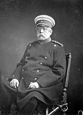
Otto von Bismarck, a German statesman often associated with Realpolitik

In the United States, the term is often analogous to power politics while in Germany Realpolitik has a somewhat less negative connotation, referring to realistic politics in opposition to idealistic (or unrealistic) politics. It is particularly associated with the era of 19th century nationalism. Realpolitik policies were employed in response to the failed revolutions of 1848 as means to strengthen states and tighten social order.

"Politics is the art of the possible."
– Bismarck, 1867 interview

The most famous German advocate of Realpolitik, what was uniquely possible and the applied means to achieve it, was Otto von Bismarck, the first Chancellor (1862–1890) to Wilhelm I of the Kingdom of Prussia. Bismarck used Realpolitik in his quest to achieve Prussian dominance in Germany. He manipulated political issues such as the Schleswig-Holstein Question and the Hohenzollern candidature to antagonize other countries and cause wars if necessary to attain his goals. Such policies are characteristic of Bismarck, demonstrating a pragmatic view of the "real" political world.

Another example was his willingness to adopt some social policies of the socialists such as employee insurance and pensions; in doing so, he used small changes from the top down to avoid the possibility of major change from the bottom up. Likewise, Prussia's seemingly illogical move of not demanding territory from a defeated Austria, a move that later led to the unification of Germany, is an oft-cited example of Realpolitik.

Singapore

Lee Kuan Yew, first Prime Minister of Singapore and one of the founders of the People's Action Party

Singaporean statesman Lee Kuan Yew, who served as the country's first prime minister, has been considered by many political analysts as a pragmatist for his erudite policies in his governance of Singapore. He believed that the only way Singapore could survive as a relatively small nation as compared to its neighbours was to contrast itself from them, by building up a highly effective and non-corrupt government, in addition to a civil service, under a meritocratic system. He also believed that Singapore was to stay neutral but also possess a strong military capability, believing that it serves as a guarantor of the country's independence due to its strategic position. A strong advocate for Asian values, he argued that Asian societies had different values from Western societies and that practicing such values was vital to succeed as a nation, especially as an Asian country, which includes collectivism and communitarianism.

Lee described Singapore's only natural resources as being the grit of its people as well as their strong work ethic, propelling this mindset to all ethnic groups of the country. Although Lee supported left-wing ideas in his young adulthood, he was largely conservative as a leader, concluding that extensive state welfare and subsidies blunted the individual's drive to succeed. Nevertheless, his government still enacted social policies, which included free public education up until at least secondary school, state housing, a compulsory comprehensive savings and pension plan, as well as universal healthcare, in addition to a civic nationalist stance.

In 1975, Chan Heng Chee described Singapore as a depoliticized "administrative state", where ideology and politics had triumphantly been replaced by "rational and scientific modes of public administration". It is suggested that by doggedly describing itself as pragmatic, the Singaporean state is actually disguising its ideological work and political nature through an assertion of the absence of ideology and politics. Chua Beng Huat argued in 1995 that the rhetoric of pragmatism in Singapore is ideological and hegemonic in nature, adopted and disseminated in the public sphere by the People's Action Party government and institutionalized throughout the state in all its administrative, planning and policy-making functions.

Many world leaders affirmed Lee's political knowledge as being pragmatist and "insightful". Former President of the United States, Barack Obama, stated that he "personally appreciated [Lee's] wisdom." Former Prime Minister of Japan, Shinzo Abe, who had also championed for Asian values, stated that Lee was "one of the greatest leaders of modern times that Asia has ever produced" and a "great Asian leader who laid the foundation for the prosperity of Singapore today." Former Prime Minister of Australia, Tony Abbott, mentioned that Lee was a "giant of our region" and that "thanks to his vision and determination, Singapore is one of the world's most successful countries." Henry Kissinger described Lee as one of the "world's most successful pragmatists". Today, his ideologies and views are now taught at the Lee Kuan Yew School of Public Policy, an autonomous postgraduate school of the National University of Singapore.

United Kingdom

E. H. Carr was a liberal realist and left-wing British historian and international relations theorist who argued for realistic international over utopian policies. Carr described realism as the acceptance that what exists is right; he thus argued that in politics, realism meant that there is no moral dimension and that what is successful is right and what is unsuccessful is wrong. Carr was convinced that the Bolsheviks were destined to win the Russian Civil War and, under the grounds of Realpolitik, approved of British Prime Minister David Lloyd George's opposition to War Secretary Winston Churchill's support for military help to the anti-Bolshevik White movement. In Carr's opinion, Churchill's support of the anti-Bolsheviks was folly, as Russia was likely to be a great power once more under the leadership of the Bolsheviks.

United States

Zbigniew Brzezinski

American Realpolitik began in the 1960s with the influence of Polish-American Zbigniew Brzezinski, later National Security Adviser to Jimmy Carter. Contrary to McCarthy-era hostility and John Foster Dulles's talk of the military "liberation" of the Eastern Bloc, Brzezinski proposed "peaceful engagement" with the Soviet Union while he advised Presidents John F. Kennedy and Lyndon B. Johnson. Brzezinski, uninterested in promoting anti-Soviet propaganda for the benefit of the United States, felt the United States would be more successful through frequent interactions with regimes and people under communist rule. Brzezinski knew the tough economic realities of those living in the Eastern Bloc, particularly the permanent shortage of goods, and that their attachment to the Soviet Union was born of historic necessity, rather than common ideology. Brzezinski suggested enticing these countries economically and through educational and cultural exchanges, which would appeal to intellectuals, followed by favoritism for regimes showing signs of liberalization or less reliance on Moscow. Through that approach, Brzezinski "offered a realistic, evolutionary alternative to empty political rhetoric."

Henry Kissinger has been credited with formally introducing the policy of Realpolitik to the White House as Secretary of State to Richard Nixon. In that context, the policy meant dealing with other powerful nations in a practical manner, rather than on the basis of political doctrine or ethics such as Nixon's diplomacy with the People's Republic of China despite American opposition to communism and the previous doctrine of containment. Another example is Kissinger's use of shuttle diplomacy after the 1973 Arab-Israeli war, when he persuaded the Israelis to withdraw partially from the Sinai in deference to the political realities created by the oil crisis.

Kissinger himself said that he had never used the term Realpolitik and stated that it is used by both liberal and realist foreign policy thinkers to label, criticize and facilitate a choosing of sides. Kissinger had looked at what he implemented while he served as Secretary of State and National Security Advisor not in the confines of making Realpolitik a standard policy, but within the terms of being a statesman. That political mindset can be seen in Kissinger's book A World Restored and was pointed out by historian John Bew in his book Realpolitik. Kissinger went on to say that the role of the statesman is "the ability to recognize the real relationship of forces and to make this knowledge serve his ends."

In that context, one can see how Realpolitik principles can influence American policy but not as standard policy. The reach and influence of Realpolitik is found instead in pragmatic and flexible policy that changes to the needs of the situation. That type of policymaking could be seen as recently as in the administration of Barack Obama. Bew made note of that direction in the Obama administration, when Obama's chief of staff, Rahm Emanuel, remarked in an article in The New York Times that everyone wanted to break it down into contrasts of idealist and realist, but "if you had to put him in a category, he's probably more realpolitik, like Bush 41 [...] You’ve got to be cold-blooded about the self-interests of your nation."

Realpolitik is distinct from ideological politics in that it is not dictated by a fixed set of rules but instead tends to be goal-oriented, limited only by practical exigencies. Since Realpolitik is ordered toward the most practical means of securing national interests, it can often entail compromising on ideological principles. For example, during the Cold War, the United States often supported authoritarian regimes that were human rights violators to secure theoretically the greater national interest of regional stability. After the end of the Cold War, this practice continued.

Most recently, former Ambassador Dennis Ross advocated that approach to foreign policy in his 2007 book Statecraft: And How to Restore America's Standing in the World. For the purposes of contrast and speaking in ideal types, political ideologues would tend to favor principle over other considerations. Such individuals or groups can reject compromises that they see as the abandonment of their ideals and so may sacrifice political gain, in favor of adhering to principles that they believe to be constitutive of long-term goals.

Pakistan

Muhammad Zia-ul-Haq

The relations of Pakistan and the US were strained during the 1970s due to Pakistan's nuclear program and the controversial execution of President Zulfikar Ali Bhutto.

In the context of Iranian Revolution, President Jimmy Carter desired to improve relations with Pakistan. General Muhammad Zia-ul-haq came into power in 1977 after Martial Law was imposed in the country due to political turmoil. Zia recognized the immediate strategic interests that Pakistan may obtain by aligning with the US amidst the Soviet-Afghan War.

Pakistan due to its strategic geopolitical location made it a subject of grave interest to the US, which supported Pakistan with financial and military assistance including General Dynamics F-16 Fighting Falcon and financial aid during the Soviet–Afghan War.

Zia initially declined the 400 million USD aid offered by US (under the Carter presidency) dismissing it as "peanuts". However when Ronald Reagan resumed office and sought to increment the funding for Operation Cyclone and aid for Pakistan, The US and Pakistan agreed on a 3.2 Billion USD military and economic aid package.

Under Zia's Leadership Pakistan played a pivotal role in training Afghan mujahidin, in conjunction with Operation Cyclone to oppose the soviet-backed government in Afghanistan.

While Pakistan was aligned with the United states, it did maintain diplomatic presence with the Soviet Union during the Afghan war which was primarily based upon pragmatic diplomacy rather than genuine partnership.

One of the major Realpolitik decision of Zia ul Haq's presidency was his role in the Nuclear program of Pakistan. Amidst international pressure, he ignored threats of sanctions and prioritized the national interest over non-proliferation international norms. The development of nuclear weapons was seen as crucial for Deterrence against Pakistan's historical rival, India which had successfully conducted nuclear tests in 1974.

Direct and indirect band gaps

In semiconductor physics, the band gap of a semiconductor can be of two basic types, a direct band gap or an indirect band gap. The minimal-energy state in the conduction band and the maximal-energy state in the valence band are each characterized by a certain crystal momentum (k-vector) in the Brillouin zone. If the k-vectors are different, the material has an "indirect gap". The band gap is called "direct" if the crystal momentum of electrons and holes is the same in both the conduction band and the valence band; an electron can directly emit a photon. In an "indirect" gap, a photon cannot be emitted because the electron must pass through an intermediate state and transfer momentum to the crystal lattice.

Examples of direct bandgap materials include amorphous silicon and some III-V materials such as InAs and GaAs. Indirect bandgap materials include crystalline silicon and Ge. Some III-V materials are indirect bandgap as well, for example AlSb.

Energy vs. crystal momentum for a semiconductor with an indirect band gap, showing that an electron cannot shift from the highest-energy state in the valence band (red) to the lowest-energy state in the conduction band (green) without a change in momentum. Here, almost all of the energy comes from a photon (vertical arrow), while almost all of the momentum comes from a phonon (horizontal arrow).
Energy vs. crystal momentum for a semiconductor with a direct band gap, showing that an electron can shift from the highest-energy state in the valence band (red) to the lowest-energy state in the conduction band (green) without a change in crystal momentum. Depicted is a transition in which a photon excites an electron from the valence band to the conduction band.
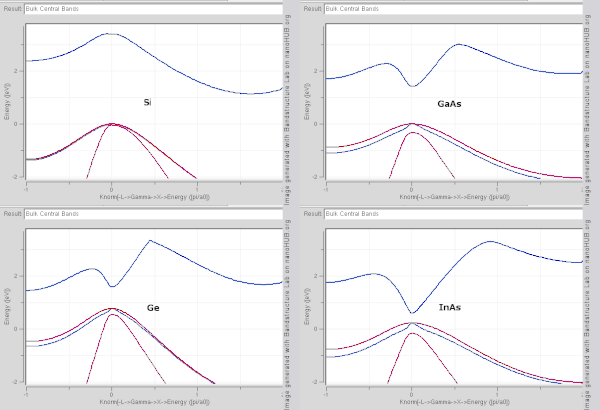
Bulk band structure for Si, Ge, GaAs and InAs generated with tight binding model. Note that Si and Ge are indirect band gap with minima at X and L, while GaAs and InAs are direct band gap materials.

Implications for radiative recombination

Interactions among electrons, holes, phonons, photons, and other particles are required to satisfy conservation of energy and crystal momentum (i.e., conservation of total k-vector). A photon with an energy near a semiconductor band gap has almost zero momentum. One important process is called radiative recombination, where an electron in the conduction band annihilates a hole in the valence band, releasing the excess energy as a photon. This is possible in a direct band gap semiconductor if the electron has a k-vector near the conduction band minimum (the hole will share the same k-vector), but not possible in an indirect band gap semiconductor, as photons cannot carry crystal momentum, and thus conservation of crystal momentum would be violated. For radiative recombination to occur in an indirect band gap material, the process must also involve the absorption or emission of a phonon, where the phonon momentum equals the difference between the electron and hole momentum. It can also, instead, involve a crystallographic defect, which performs essentially the same role. The involvement of the phonon makes this process much less likely to occur in a given span of time, which is why radiative recombination is far slower in indirect band gap materials than direct band gap ones. This is why light-emitting and laser diodes are almost always made of direct band gap materials, and not indirect band gap ones like silicon.

The fact that radiative recombination is slow in indirect band gap materials also means that, under most circumstances, radiative recombinations will be a small proportion of total recombinations, with most recombinations being non-radiative, taking place at point defects or at grain boundaries. However, if the excited electrons are prevented from reaching these recombination places, they have no choice but to eventually fall back into the valence band by radiative recombination. This can be done by creating a dislocation loop in the material.[clarification needed] At the edge of the loop, the planes above and beneath the "dislocation disk" are pulled apart, creating a negative pressure, which raises the energy of the conduction band substantially, with the result that the electrons cannot pass this edge. Provided that the area directly above the dislocation loop is defect-free (no non-radiative recombination possible), the electrons will fall back into the valence shell by radiative recombination, thus emitting light. This is the principle on which "DELEDs" (Dislocation Engineered LEDs) are based.

Implications for light absorption

The exact reverse of radiative recombination is light absorption. For the same reason as above, light with a photon energy close to the band gap can penetrate much farther before being absorbed in an indirect band gap material than a direct band gap one (at least insofar as the light absorption is due to exciting electrons across the band gap).

This fact is very important for photovoltaics (solar cells). Crystalline silicon is the most common solar-cell substrate material, despite the fact that it is indirect-gap and therefore does not absorb light very well. As such, they are typically hundreds of microns thick; thinner wafers would allow much of the light (particularly in longer wavelengths) to simply pass through. By comparison, thin-film solar cells are made of direct band gap materials (such as amorphous silicon, CdTe, CIGS or CZTS), which absorb the light in a much thinner region, and consequently can be made with a very thin active layer (often less than 1 micron thick).

The absorption spectrum of an indirect band gap material usually depends more on temperature than that of a direct material, because at low temperatures there are fewer phonons, and therefore it is less likely that a photon and phonon can be simultaneously absorbed to create an indirect transition. For example, silicon is opaque to visible light at room temperature, but transparent to red light at liquid helium temperatures, because red photons can only be absorbed in an indirect transition.

Formula for absorption

A common and simple method for determining whether a band gap is direct or indirect uses absorption spectroscopy. By plotting certain powers of the absorption coefficient against photon energy, one can normally tell both what value the band gap is, and whether or not it is direct.

For a direct band gap, the absorption coefficient is related to light frequency according to the following formula:

, with

where:

This formula is valid only for light with photon energy larger, but not too much larger, than the band gap (more specifically, this formula assumes the bands are approximately parabolic), and ignores all other sources of absorption other than the band-to-band absorption in question, as well as the electrical attraction between the newly created electron and hole (see exciton). It is also invalid in the case that the direct transition is forbidden, or in the case that many of the valence band states are empty or conduction band states are full.

On the other hand, for an indirect band gap, the formula is:

where:

This formula involves the same approximations mentioned above.

Therefore, if a plot of versus forms a straight line, it can normally be inferred that there is a direct band gap, measurable by extrapolating the straight line to the axis. On the other hand, if a plot of versus forms a straight line, it can normally be inferred that there is an indirect band gap, measurable by extrapolating the straight line to the axis (assuming ).

Other aspects

In some materials with an indirect gap, the value of the gap is negative. The top of the valence band is higher than the bottom of the conduction band in energy. Such materials are known as semimetals.

Crystalline silicon

From Wikipedia, the free encyclopedia
Crystalline-silicon solar cells are made of either Poly Silicon (left side) or Mono Silicon (right side).

Crystalline silicon or (c-Si) Is the crystalline forms of silicon, either polycrystalline silicon (poly-Si, consisting of small crystals), or monocrystalline silicon (mono-Si, a continuous crystal). Crystalline silicon is the dominant semiconducting material used in photovoltaic technology for the production of solar cells. These cells are assembled into solar panels as part of a photovoltaic system to generate solar power from sunlight.

In electronics, crystalline silicon is typically the monocrystalline form of silicon, and is used for producing microchips. This silicon contains much lower impurity levels than those required for solar cells. Production of semiconductor grade silicon involves a chemical purification to produce Hyper-pure Polysilicon, followed by a recrystallization process to grow monocrystalline silicon. The cylindrical boules are then cut into wafers for further processing.

Solar cells made of crystalline silicon are often called conventional, traditional, or first generation solar cells, as they were developed in the 1950s and remained the most common type up to the present time. Because they are produced from 160 to 190 μm thick solar wafers—slices from bulks of solar grade silicon—they are sometimes called wafer-based solar cells.

Solar cells made from c-Si are single-junction cells and are generally more efficient than their rival technologies, which are the second-generation thin-film solar cells, the most important being CdTe, CIGS, and amorphous silicon (a-Si). Amorphous silicon is an allotropic variant of silicon, and amorphous means "without shape" to describe its non-crystalline form.

Overview

Global PV market by technology in 2021.

  CdTe (4.1%)
  a-Si (0.1%)
  CIGS (0.8%)
  mono-Si (82%)
  multi-Si (13%)

Classification

The allotropic forms of silicon range from a single crystalline structure to a completely unordered amorphous structure with several intermediate varieties. In addition, each of these different forms can possess several names and even more abbreviations, and often cause confusion to non-experts, especially as some materials and their application as a PV technology are of minor significance, while other materials are of outstanding importance.

PV industry

In photovoltaic industry, materials are commonly grouped into the following two categories:

Generations

Alternatively, different types of solar cells and/or their semiconducting materials can be classified by generations:

  • First generation solar cells are made of crystalline silicon, also called, conventional, traditional, wafer-based solar cells and include monocrystalline (mono-Si) and polycrystalline (multi-Si) semiconducting materials.
  • Second generation solar cells or panels are based on thin-film technology and are of commercially significant importance. These include CdTe, CIGS and amorphous silicon.
  • Third generation solar cells are often labeled as emerging technologies with little or no market significance and include a large range of substances, mostly organic, often using organometallic compounds.

Arguably, multi-junction photovoltaic cells can be classified to neither of these generations. A typical triple junction semiconductor is made of InGaP/(In)GaAs/Ge.

Comparison of technical specifications

Categories Technology η (%) VOC (V) ISC (A) W/m2 t (μm)
Thin-film solar cells
a-Si 11.1 6.3 0.0089 33 1
CdTe 16.5 0.86 0.029 5
CIGS 20.5

Market share

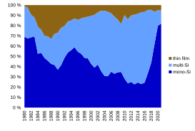
Global Photovoltaics market share by technology 1980–2021.

In 2013, conventional crystalline silicon technology dominated worldwide PV production, with multi-Si leading the market ahead of mono-Si, accounting for 54% and 36%, respectively. For the last ten years, worldwide market-share of thin-film technologies stagnated below 18% and currently stand at 9%. In the thin-film market, CdTe leads with an annual production of 2 GWp or 5%, followed by a-Si and CIGS, both around 2%. Alltime deployed PV capacity of 139 gigawatts (cumulative as of 2013) splits up into 121 GW crystalline silicon (87%) and 18 GW thin-film (13%) technology.

Efficiency

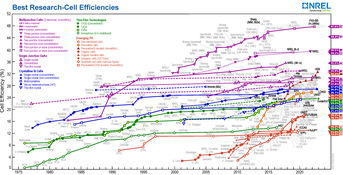
Conversion Efficiencies of best research solar cells worldwide for various Photovoltaic Technologies since 1976.

The conversion efficiency of PV devices describes the energy-ratio of the outgoing electrical power compared to the incoming radiated light. A single solar cells has generally a better, or higher efficiency than an entire solar module. Additionally, lab efficiency is always far superior to that of goods that are sold commercially.

Lab cells

In 2013, record Lab cell efficiency was highest for crystalline silicon. However, multi-silicon is followed closely by cadmium telluride and copper indium gallium selenide solar cells.

  1. 25.6% ------- mono-Si cell
  2. 20.4% -------- multi-Si cell
  3. 21.7% ----------- CIGS cell
  4. 21.5% ----------- CdTe cell

Both-sides-contacted silicon solar cells as of 2021: 26% and possibly above.

Modules

The average commercial crystalline silicon module increased its efficiency from about 12% to 16% over the last ten years. In the same period CdTe-modules improved their efficiency from 9 to 16%. The modules performing best under lab conditions in 2014 were made of monocrystalline silicon. They were 7% above the efficiency of commercially produced modules (23% over 16%) which indicated that the conventional silicon technology still had potential to improve and therefore maintain its leading position.

Energy costs of manufacture

Crystalline silicon has a high cost in energy because silicon is produced by the reduction of high-grade quartz sand in an electric furnace. The electricity generated for this process may produce greenhouse gas emissions. This coke-fired smelting process occurs at high temperatures of more than 1,000 °C and is very energy intensive, using about 11 kilowatt-hours (kWh) per kilogram of silicon.

The energy requirements of this process per unit of silicon metal produced may be relatively inelastic. But major energy cost reductions per (photovoltaic) product have been made as silicon cells have become more efficient at converting sunlight, larger silicon metal ingots are cut with less waste into thinner wafers, silicon waste from manufacture is recycled, and material costs have reduced.

Toxicity

With the exception of amorphous silicon, most commercially established PV technologies use toxic heavy metals. CIGS often uses a CdS buffer layer, and the semiconductor material of CdTe-technology itself contains the toxic cadmium (Cd). In the case of crystalline silicon modules, the solder material that joins the copper strings of the cells, it contains about 36% of lead (Pb). Moreover, the paste used for screen printing front and back contacts contains traces of Pb and sometimes Cd as well. It is estimated that about 1,000 metric tonnes of Pb have been used for 100 gigawatts of c-Si solar modules. However, there is no fundamental need for lead in the solder alloy.

Cell technologies

PERC solar cell

Passivated emitter rear contact (PERC) solar cells  consist of the addition of an extra layer to the rear-side of a solar cell. This dielectric passive layer acts to reflect unabsorbed light back to the solar cell for a second absorption attempt increasing the solar cell efficiency.

A PERC is created through an additional film deposition and etching process. Etching can be done either by chemical or laser processing. About 80% of solar panels worldwide use the PERC design. Martin Green, Andrew Blakers, Jianhua Zhao and Aihua Wang won the Queen Elizabeth Prize for Engineering in 2023 for development of the PERC solar cell.

HIT solar cell

Schematics of a HIT-cell...

A HIT solar cell is composed of a mono thin crystalline silicon wafer surrounded by ultra-thin amorphous silicon layers. The acronym HIT stands for "heterojunction with intrinsic thin layer". HIT cells are produced by the Japanese multinational electronics corporation Panasonic (see also Sanyo § Solar cells and plants). Panasonic and several other groups have reported several advantages of the HIT design over its traditional c-Si counterpart:

1. An intrinsic a-Si layer can act as an effective surface passivation layer for c-Si wafer.

2. The p+/n+ doped a-Si functions as an effective emitter/BSF for the cell.

3. The a-Si layers are deposited at much lower temperature, compared to the processing temperatures for traditional diffused c-Si technology.

4. The HIT cell has a lower temperature coefficient compared to c-Si cell technology.

Owing to all these advantages, this new hetero-junction solar cell is a considered to be a promising low cost alternative to traditional c-Si based solar cells.

Fabrication of HIT cells

The details of the fabrication sequence vary from group to group. Typically in good quality, CZ/FZ grown c-Si wafer (with ~1ms lifetimes) are used as the absorber layer of HIT cells. Using alkaline etchants, such as, NaOH or (CH3)4NOH the (100) surface of the wafer is textured to form the pyramids of 5-10μm height. Next, the wafer is cleaned using peroxide and HF solutions. This is followed by deposition of intrinsic a-Si passivation layer, typically through PECVD or Hot-wire CVD. The silane (SiH4) gas diluted with H2 is used as a precursor. The deposition temperature and pressure is maintained at 200o C and 0.1-1 Torr. Precise control over this step is essential to avoid the formation of defective epitaxial Si.

Cycles of deposition and annealing and H2 plasma treatment are shown to have provided excellent surface passivation. Diborane or Trimethylboron gas mixed with SiH4 is used to deposit p-type a-Si layer, while, Phosphine gas mixed with SiH4 is used to deposit n-type a-Si layer. Direct deposition of doped a-Si layers on c-Si wafer is shown to have very poor passivation properties. This is most likely due to dopant induced defect generation in a-Si layers. Sputtered Indium Tin Oxide (ITO) is commonly used as a transparent conductive oxide (TCO) layer on top of the front and back a-Si layer in bi-facial design, as a-Si has high lateral resistance.

It is generally deposited on the back side as well fully metallized cell to avoid diffusion of back metal and also for impedance matching for the reflected light. The silver/aluminum grid of 50-100μm thick is deposited through stencil printing for the front contact and back contact for bi-facial design. The detailed description of the fabrication process can be found in.

Opto-electrical modeling and characterization of HIT cells

The literature discusses several studies to interpret carrier transport bottlenecks in these cells. Traditional light and dark I-V are extensively studied  and are observed to have several non-trivial features, which cannot be explained using the traditional solar cell diode theory. This is because of the presence of hetero-junction between the intrinsic a-Si layer and c-Si wafer which introduces additional complexities to current flow. In addition, there has been significant efforts to characterize this solar cell using C-V, impedance spectroscopy, surface photo-voltage, suns-Voc to produce complementary information.

Further, a number of design improvements, such as, the use of new emitters, bifacial configuration, interdigitated back contact (IBC) configuration bifacial-tandem configuration are actively being pursued.

Mono-silicon

Schematic of allotropic forms of silicon.

Monocrystalline silicon (mono c-Si) is a form in which the crystal structure is homogeneous throughout the material; the orientation, lattice parameter, and electronic properties are constant throughout the material. Dopant atoms such as phosphorus and boron are often incorporated into the film to make the silicon n-type or p-type respectively. Monocrystalline silicon is fabricated in the form of silicon wafers, usually by the Czochralski Growth method, and can be quite expensive depending on the radial size of the desired single crystal wafer (around $200 for a 300 mm Si wafer). This monocrystalline material, while useful, is one of the chief expenses associated with producing photovoltaics where approximately 40% of the final price of the product is attributable to the cost of the starting silicon wafer used in cell fabrication.

Polycrystalline silicon

Polycrystalline silicon is composed of many smaller silicon grains of varied crystallographic orientation, typically >1 mm in size. This material can be synthesized easily by allowing liquid silicon to cool using a seed crystal of the desired crystal structure. Additionally, other methods for forming smaller-grained polycrystalline silicon (poly-Si) exist such as high temperature chemical vapor deposition (CVD).

Not classified as Crystalline silicon

These allotropic forms of silicon are not classified as crystalline silicon. They belong to the group of thin-film solar cells.

Amorphous silicon

Amorphous silicon (a-Si) has no long-range periodic order. The application of amorphous silicon to photovoltaics as a standalone material is somewhat limited by its inferior electronic properties. When paired with microcrystalline silicon in tandem and triple-junction solar cells, however, higher efficiency can be attained than with single-junction solar cells. This tandem assembly of solar cells allows one to obtain a thin-film material with a bandgap of around 1.12 eV (the same as single-crystal silicon) compared to the bandgap of amorphous silicon of 1.7-1.8 eV bandgap. Tandem solar cells are then attractive since they can be fabricated with a bandgap similar to single-crystal silicon but with the ease of amorphous silicon.

Nanocrystalline silicon

Nanocrystalline silicon (nc-Si), sometimes also known as microcrystalline silicon (μc-Si), is a form of porous silicon. It is an allotropic form of silicon with paracrystalline structure—is similar to amorphous silicon (a-Si), in that it has an amorphous phase. Where they differ, however, is that nc-Si has small grains of crystalline silicon within the amorphous phase. This is in contrast to polycrystalline silicon (poly-Si) which consists solely of crystalline silicon grains, separated by grain boundaries. The difference comes solely from the grain size of the crystalline grains. Most materials with grains in the micrometre range are actually fine-grained polysilicon, so nanocrystalline silicon is a better term. The term Nanocrystalline silicon refers to a range of materials around the transition region from amorphous to microcrystalline phase in the silicon thin film.

Protocrystalline silicon

Protocrystalline silicon has a higher efficiency than amorphous silicon (a-Si) and it has also been shown to improve stability, but not eliminate it. A Protocrystalline phase is a distinct phase occurring during crystal growth which evolves into a microcrystalline form.

Protocrystalline Si also has a relatively low absorption near the band gap owing to its more ordered crystalline structure. Thus, protocrystalline and amorphous silicon can be combined in a tandem solar cell where the top layer of thin protocrystalline silicon absorbs short-wavelength light whereas the longer wavelengths are absorbed by the underlying a-Si substrate.

Transformation of amorphous into crystalline silicon

Amorphous silicon can be transformed to crystalline silicon using well-understood and widely implemented high-temperature annealing processes. The typical method used in industry requires high-temperature compatible materials, such as special high temperature glass that is expensive to produce. However, there are many applications for which this is an inherently unattractive production method.

Low temperature induced crystallization

Flexible solar cells have been a topic of interest for less conspicuous-integrated power generation than solar power farms. These modules may be placed in areas where traditional cells would not be feasible, such as wrapped around a telephone pole or cell phone tower. In this application, a photovoltaic material may be applied to a flexible substrate, often a polymer. Such substrates cannot survive the high temperatures experienced during traditional annealing. Instead, novel methods of crystallizing the silicon without disturbing the underlying substrate have been studied extensively. Aluminum-induced crystallization (AIC) and local laser crystallization are common in the literature, however not extensively used in industry.

In both of these methods, amorphous silicon is grown using traditional techniques such as plasma-enhanced chemical vapor deposition (PECVD). The crystallization methods diverge during post-deposition processing. In aluminum-induced crystallization, a thin layer of aluminum (50 nm or less) is deposited by physical vapor deposition onto the surface of the amorphous silicon. This stack of material is then annealed at a relatively low temperature between 140 °C and 200 °C in a vacuum. The aluminum that diffuses into the amorphous silicon is believed to weaken the hydrogen bonds present, allowing crystal nucleation and growth. Experiments have shown that polycrystalline silicon with grains on the order of 0.2 – 0.3 μm can be produced at temperatures as low as 150 °C. The volume fraction of the film that is crystallized is dependent on the length of the annealing process.

Aluminum-induced crystallization produces polycrystalline silicon with suitable crystallographic and electronic properties that make it a candidate for producing polycrystalline thin films for photovoltaics. AIC can be used to generate crystalline silicon nanowires and other nano-scale structures.

Another method of achieving the same result is the use of a laser to heat the silicon locally without heating the underlying substrate beyond some upper-temperature limit. An excimer laser or, alternatively, green lasers such as a frequency-doubled Nd:YAG laser is used to heat the amorphous silicon, supplying the energy necessary to nucleate grain growth. The laser fluence must be carefully controlled in order to induce crystallization without causing widespread melting. Crystallization of the film occurs as a very small portion of the silicon film is melted and allowed to cool. Ideally, the laser should melt the silicon film through its entire thickness, but not damage the substrate. Toward this end, a layer of silicon dioxide is sometimes added to act as a thermal barrier. This allows the use of substrates that cannot be exposed to the high temperatures of standard annealing, polymers for instance. Polymer-backed solar cells are of interest for seamlessly integrated power production schemes that involve placing photovoltaics on everyday surfaces.

A third method for crystallizing amorphous silicon is the use of a thermal plasma jet. This strategy is an attempt to alleviate some of the problems associated with laser processing – namely the small region of crystallization and the high cost of the process on a production scale. The plasma torch is a simple piece of equipment that is used to anneal the amorphous silicon thermally. Compared to the laser method, this technique is simpler and more cost-effective. Plasma torch annealing is attractive because the process parameters and equipment dimensions can be changed easily to yield varying levels of performance. A high level of crystallization (~90%) can be obtained with this method. Disadvantages include difficulty achieving uniformity in the crystallization of the film. While this method is applied frequently to silicon on a glass substrate, processing temperatures may be too high for polymers.

Lie point symmetry

From Wikipedia, the free encyclopedia https://en.wikipedia.org/wiki/Lie_point_symmetry     ...