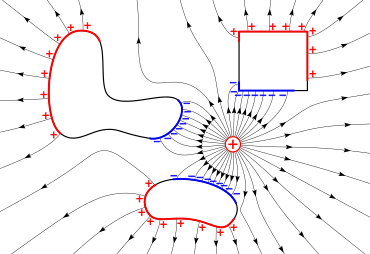
Electric field of a positive point electric charge suspended over an infinite sheet of conducting material. The field is depicted by electric field lines, lines which follow the direction of the electric field in space.
An electric field surrounds an electric charge, and exerts force on other charges in the field, attracting or repelling them. Electric field is sometimes abbreviated as E-field. The electric field is defined mathematically as a vector field that associates to each point in space the (electrostatic or Coulomb) force per unit of charge exerted on an infinitesimal positive test charge at rest at that point. The SI unit for electric field strength is volt per meter (V/m). Newtons per coulomb (N/C) is also used as a unit of electric field strength. Electric fields are created by electric charges, or by time-varying magnetic fields. Electric fields are important in many areas of physics,
and are exploited practically in electrical technology. On an atomic
scale, the electric field is responsible for the attractive force
between the atomic nucleus and electrons that holds atoms together, and the forces between atoms that cause chemical bonding. Electric fields and magnetic fields are both manifestations of the electromagnetic force, one of the four fundamental forces (or interactions) of nature.
Definition
From Coulomb's law a particle with electric charge at position exerts a force on a particle with charge at position of
where is the unit vector in the direction from point to point , and ε0 is the electric constant (also known as "the absolute permittivity of free space") in C2 m−2 N−1
When the charges and
have the same sign this force is positive, directed away from the other
charge, indicating the particles repel each other. When the charges
have unlike signs the force is negative, indicating the particles
attract.
To make it easy to calculate the Coulomb force on any charge at position this expression can be divided by , leaving an expression that only depends on the other charge (the source charge)
This is the electric field at point due to the point charge ; it is a vector equal to the Coulomb force per unit charge that a positive point charge would experience at the position .
Since this formula gives the electric field magnitude and direction at any point in space (except at the location of the charge itself, , where it becomes infinite) it defines a vector field.
From the above formula it can be seen that the electric field due to a
point charge is everywhere directed away from the charge if it is
positive, and toward the charge if it is negative, and its magnitude
decreases with the inverse square of the distance from the charge.
If there are multiple charges, the resultant Coulomb force on a
charge can be found by summing the vectors of the forces due to each
charge. This shows the electric field obeys the superposition principle:
the total electric field at a point due to a collection of charges is
just equal to the vector sum of the electric fields at that point due to
the individual charges.
where is the unit vector in the direction from point to point .
This is the definition of the electric field due to the point source charges.
It diverges and becomes infinite at the locations of the charges themselves, and so is not defined there.
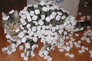
Evidence of an electric field: styrofoam peanuts clinging to a cat's fur due to static electricity. The triboelectric effect causes an electrostatic charge
to build up on the fur due to the cat's motions. The electric field of
the charge causes polarization of the molecules of the styrofoam due to electrostatic induction, resulting in a slight attraction of the light plastic pieces to the charged fur. This effect is also the cause of static cling in clothes.
The Coulomb force on a charge of magnitude at any point in space is equal to the product of the charge and the electric field at that point
The units of the electric field in the SI system are newtons per coulomb (N/C), or volts per meter (V/m); in terms of the SI base units they are kg⋅m⋅s−3⋅A−1
The electric field due to a continuous distribution of charge in space (where is the charge density in coulombs per cubic meter) can be calculated by considering the charge in each small volume of space at point as a point charge, and calculating its electric field at point
where is the unit vector pointing from to , then adding up the contributions from all the increments of volume by integrating over the volume of the charge distribution
Sources
Causes and description
Electric fields are caused by electric charges, described by Gauss's law, or varying magnetic fields, described by Faraday's law of induction. Together, these laws are enough to define the behavior of the electric field as a function of charge repartition
and magnetic field. However, since the magnetic field is described as a
function of electric field, the equations of both fields are coupled
and together form Maxwell's equations that describe both fields as a function of charges and currents.
In the special case of a steady state (stationary charges and currents), the Maxwell-Faraday inductive effect disappears. The resulting two equations (Gauss's law and Faraday's law with no induction term ), taken together, are equivalent to Coulomb's law, written as for a charge density ( is position in space). Notice that , the vacuum electric permittivity, must be substituted with , permittivity, when charges are in non-empty media.
Continuous vs. discrete charge representation
The electric field (lines with arrows) of a charge (+) induces surface charges (red and blue areas) on metal objects due to electrostatic induction.
The equations of electromagnetism are best described in a continuous
description. However, charges are sometimes best described as discrete
points; for example, some models may describe electrons as point sources where charge density is infinite on an infinitesimal section of space.
A charge located at can be described mathematically as a charge density , where the Dirac delta function (in three dimensions) is used. Conversely, a charge distribution can be approximated by many small point charges.
Superposition principle
Electric fields satisfy the superposition principle, because Maxwell's equations are linear. As a result, if and are the electric fields resulting from distribution of charges and , a distribution of charges will create an electric field ; for instance, Coulomb's law is linear in charge density as well.
This principle is useful to calculate the field created by multiple point charges. If charges are stationary in space at ,
in the absence of currents, the superposition principle proves that the
resulting field is the sum of fields generated by each particle as
described by Coulomb's law:
Electrostatic fields
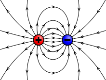
Illustration of the electric field surrounding a positive (red) and a negative (blue) charge
Electrostatic fields are electric fields which do not change with
time, which happens when charges and currents are stationary. In that
case, Coulomb's law fully describes the field.
Electric potential
If a system is static, such that magnetic fields are not
time-varying, then by Faraday's law, the electric field is curl-free. In
this case, one can define an electric potential, that is, a function such that .
This is analogous to the gravitational potential.
Parallels between electrostatic and gravitational fields
Coulomb's law, which describes the interaction of electric charges:
This suggests similarities between the electric field E and the gravitational field g, or their associated potentials. Mass is sometimes called "gravitational charge".
A uniform field is one in which the electric field is constant at every point. It can be approximated by placing two conducting plates parallel to each other and maintaining a voltage
(potential difference) between them; it is only an approximation
because of boundary effects (near the edge of the planes, electric field
is distorted because the plane does not continue). Assuming infinite
planes, the magnitude of the electric field E is:
where ΔV is the potential difference between the plates and d
is the distance separating the plates. The negative sign arises as
positive charges repel, so a positive charge will experience a force
away from the positively charged plate, in the opposite direction to
that in which the voltage increases. In micro- and nano-applications,
for instance in relation to semiconductors, a typical magnitude of an
electric field is in the order of 106 V⋅m−1, achieved by applying a voltage of the order of 1 volt between conductors spaced 1 µm apart.
Electrodynamic fields
Electrodynamic fields are electric fields which do change with time, for instance when charges are in motion.
The electric field cannot be described independently of the magnetic field in that case. If A is the magnetic vector potential, defined so that , one can still define an electric potential such that:
where ε is the permittivity of the medium in which the field exists, its magnetic permeability, and E and B are the electric and magnetic field vectors.
As E and B fields are coupled, it would be
misleading to split this expression into "electric" and "magnetic"
contributions. However, in the steady-state case, the fields are no
longer coupled. It makes sense in that case to compute the electrostatic energy per unit volume:
The total energy U stored in the electric field in a given volume V is therefore
Further extensions
Definitive equation of vector fields
In the presence of matter, it is helpful to extend the notion of the electric field into three vector fields:
where P is the electric polarization – the volume density of electric dipole moments, and D is the electric displacement field. Since E and P are defined separately, this equation can be used to define D. The physical interpretation of D is not as clear as E (effectively the field applied to the material) or P
(induced field due to the dipoles in the material), but still serves as
a convenient mathematical simplification, since Maxwell's equations can
be simplified in terms of free charges and currents.
Constitutive relation
The E and D fields are related by the permittivity of the material, ε.
For linear, homogeneous, isotropic materials E and D
are proportional and constant throughout the region, there is no
position dependence: For inhomogeneous materials, there is a position
dependence throughout the material:
For anisotropic materials the E and D fields are not parallel, and so E and D are related by the permittivity tensor (a 2nd order tensor field), in component form:
For non-linear media, E and D are not proportional. Materials can have varying extents of linearity, homogeneity and isotropy.
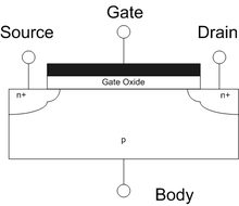
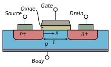
Cross-sectional view of a field-effect transistor, showing source, gate and drain terminals
The field-effect transistor (FET) is a type of transistor which uses an electric field to control the flow of current. FETs are devices with three terminals: source, gate, and drain. FETs control the flow of current by the application of a voltage to the gate, which in turn alters the conductivity between the drain and source.
FETs are also known as unipolar transistors since they involve single-carrier-type operation. That is, FETs use electrons or holes as charge carriers
in their operation, but not both. Many different types of field effect
transistors exist. Field effect transistors generally display very high input impedance at low frequencies. The most widely used field-effect transistor is the MOSFET (metal-oxide-semiconductor field-effect transistor).
The concept of a field-effect transistor (FET) was first patented by Austro-Hungarian physicist Julius Edgar Lilienfeld in 1925 and by Oskar Heil in 1934, but they were unable to build a working practical semiconducting device based on the concept. The transistor effect was later observed and explained by John Bardeen and Walter Houser Brattain while working under William Shockley at Bell Labs
in 1947, shortly after the 17-year patent expired. Shockley initially
attempted to build a working FET, by trying to modulate the conductivity
of a semiconductor, but was unsuccessful, mainly due to problems with the surface states, the dangling bond, and the germanium and copper
compound materials. In the course of trying to understand the
mysterious reasons behind their failure to build a working FET, this led
to Bardeen and Brattain instead building a point-contact transistor in 1947, which was followed by Shockley's bipolar junction transistor in 1948.
The first FET device to be successfully built was the junction field-effect transistor (JFET). A JFET was first patented by Heinrich Welker in 1945. The static induction transistor (SIT), a type of JFET with a short channel, was invented by Japanese engineers Jun-ichi Nishizawa
and Y. Watanabe in 1950. Following Shockley's theoretical treatment on
the JFET in 1952, a working practical JFET was built by George F. Dacey
and Ian M. Ross in 1953. However, the JFET still had issues affecting junction transistors in general. Junction transistors were relatively bulky devices that were difficult to manufacture on a mass-production
basis, which limited them to a number of specialised applications. The
insulated-gate field-effect transistor (IGFET) was theorized as a
potential alternative to junction transistors, but researchers were
unable to build working IGFETs, largely due to the troublesome surface
state barrier that prevented the external electric field from penetrating into the material. By the mid-1950s, researchers had largely given up on the FET concept, and instead focused on bipolar junction transistor (BJT) technology.
A breakthrough in FET research came with the work of Egyptian engineer Mohamed Atalla in the late 1950s. He investigated the surface properties of silicon semiconductors at Bell Labs, where he adopted a new method of semiconductor device fabrication, coating a silicon wafer with an insulating layer of silicon oxide,
so that electricity could reliably penetrate to the conducting silicon
below, overcoming the surface states that prevented electricity from
reaching the semiconducting layer. This is known as surface passivation, a method that became critical to the semiconductor industry as it made mass-production of silicon integrated circuits possible. Building on his surface passivation method, he developed the metal–oxide–semiconductor (MOS) process, which he presented in 1957.
He later proposed the MOS process could be used to build the first
working silicon FET, which he began working on building with the help of
his Korean colleague Dawon Kahng.
The metal–oxide–semiconductor field-effect transistor (MOSFET) was invented by Mohamed Atalla and Dawon Kahng in 1959. The MOSFET largely superseded both the bipolar transistor and the JFET, and had a profound effect on digital electronic development. With its high scalability, and much lower power consumption and higher density than bipolar junction transistors, the MOSFET made it possible to build high-density integrated circuits. The MOSFET is also capable of handling higher power than the JFET. The MOSFET was the first truly compact transistor that could be miniaturised and mass-produced for a wide range of uses. The MOSFET thus became the most common type of transistor in computers, electronics, and communications technology (such as smartphones). The US Patent and Trademark Office calls it a "groundbreaking invention that transformed life and culture around the world".
FETs can be majority-charge-carrier devices, in which the current is
carried predominantly by majority carriers, or minority-charge-carrier
devices, in which the current is mainly due to a flow of minority
carriers. The device consists of an active channel through which charge carriers, electrons or holes, flow from the source to the drain. Source and drain terminal conductors are connected to the semiconductor through ohmic contacts. The conductivity of the channel is a function of the potential applied across the gate and source terminals.
The FET's three terminals are:
source (S), through which the carriers enter the channel. Conventionally, current entering the channel at S is designated by IS.
drain (D), through which the carriers leave the channel. Conventionally, current entering the channel at D is designated by ID. Drain-to-source voltage is VDS.
gate (G), the terminal that modulates the channel conductivity. By applying voltage to G, one can control ID.
More about terminals
Cross section of an n-type MOSFET
All FETs have source, drain, and gate terminals that correspond roughly to the emitter, collector, and base of BJTs. Most FETs have a fourth terminal called the body, base, bulk, or substrate. This fourth terminal serves to bias
the transistor into operation; it is rare to make non-trivial use of
the body terminal in circuit designs, but its presence is important when
setting up the physical layout of an integrated circuit. The size of the gate, length L in the diagram, is the distance between source and drain. The width
is the extension of the transistor, in the direction perpendicular to
the cross section in the diagram (i.e., into/out of the screen).
Typically the width is much larger than the length of the gate. A gate
length of 1 µm limits the upper frequency to about 5 GHz, 0.2 µm to
about 30 GHz.
The names of the terminals refer to their functions. The gate
terminal may be thought of as controlling the opening and closing of a
physical gate. This gate permits electrons to flow through or blocks
their passage by creating or eliminating a channel between the source
and drain. Electron-flow from the source terminal towards the drain
terminal is influenced by an applied voltage. The body simply refers to
the bulk of the semiconductor in which the gate, source and drain lie.
Usually the body terminal is connected to the highest or lowest voltage
within the circuit, depending on the type of the FET. The body terminal
and the source terminal are sometimes connected together since the
source is often connected to the highest or lowest voltage within the
circuit, although there are several uses of FETs which do not have such a
configuration, such as transmission gates and cascode circuits.
Effect of gate voltage on current
I–V characteristics and output plot of a JFET n-channel transistor.
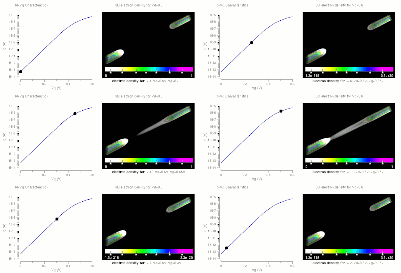
Simulation
result for right side: formation of inversion channel (electron
density) and left side: current-gate voltage curve (transfer
characteristics) in an n-channel nanowireMOSFET. Note that the threshold voltage for this device lies around 0.45 V.
FET conventional symbol types
The FET controls the flow of electrons (or electron holes)
from the source to drain by affecting the size and shape of a
"conductive channel" created and influenced by voltage (or lack of
voltage) applied across the gate and source terminals. (For simplicity,
this discussion assumes that the body and source are connected.) This
conductive channel is the "stream" through which electrons flow from
source to drain.
n-channel FET
In an n-channel "depletion-mode" device, a negative gate-to-source voltage causes a depletion region
to expand in width and encroach on the channel from the sides,
narrowing the channel. If the active region expands to completely close
the channel, the resistance of the channel from source to drain becomes
large, and the FET is effectively turned off like a switch (see right
figure, when there is very small current). This is called "pinch-off",
and the voltage at which it occurs is called the "pinch-off voltage".
Conversely, a positive gate-to-source voltage increases the channel size
and allows electrons to flow easily (see right figure, when there is a
conduction channel and current is large).
In an n-channel "enhancement-mode" device, a conductive channel
does not exist naturally within the transistor, and a positive
gate-to-source voltage is necessary to create one. The positive voltage
attracts free-floating electrons within the body towards the gate,
forming a conductive channel. But first, enough electrons must be
attracted near the gate to counter the dopant ions added to the body of
the FET; this forms a region with no mobile carriers called a depletion region, and the voltage at which this occurs is referred to as the threshold voltage
of the FET. Further gate-to-source voltage increase will attract even
more electrons towards the gate which are able to create a conductive
channel from source to drain; this process is called inversion.
p-channel FET
In a p-channel
"depletion-mode" device, a positive voltage from gate to body widens
the depletion layer by forcing electrons to the
gate-insulator/semiconductor interface, leaving exposed a carrier-free
region of immobile, positively charged acceptor ions.
Conversely, in a p-channel "enhancement-mode" device, a
conductive region does not exist and negative voltage must be used to
generate a conduction channel.
Effect of drain-to-source voltage on channel
For
either enhancement- or depletion-mode devices, at drain-to-source
voltages much less than gate-to-source voltages, changing the gate
voltage will alter the channel resistance, and drain current will be
proportional to drain voltage (referenced to source voltage). In this
mode the FET operates like a variable resistor and the FET is said to be
operating in a linear mode or ohmic mode.
If drain-to-source voltage is increased, this creates a
significant asymmetrical change in the shape of the channel due to a
gradient of voltage potential from source to drain. The shape of the
inversion region becomes "pinched-off" near the drain end of the
channel. If drain-to-source voltage is increased further, the pinch-off
point of the channel begins to move away from the drain towards the
source. The FET is said to be in saturation mode; although some authors refer to it as active mode, for a better analogy with bipolar transistor operating regions.
The saturation mode, or the region between ohmic and saturation, is
used when amplification is needed. The in-between region is sometimes
considered to be part of the ohmic or linear region, even where drain
current is not approximately linear with drain voltage.
Even though the conductive channel formed by gate-to-source voltage no longer connects source to drain during saturation mode, carriers are not blocked from flowing. Considering again an n-channel enhancement-mode device, a depletion region
exists in the p-type body, surrounding the conductive channel and drain
and source regions. The electrons which comprise the channel are free
to move out of the channel through the depletion region if attracted to
the drain by drain-to-source voltage. The depletion region is free of
carriers and has a resistance similar to silicon.
Any increase of the drain-to-source voltage will increase the distance
from drain to the pinch-off point, increasing the resistance of the
depletion region in proportion to the drain-to-source voltage applied.
This proportional change causes the drain-to-source current to remain
relatively fixed, independent of changes to the drain-to-source voltage,
quite unlike its ohmic behavior in the linear mode of operation. Thus,
in saturation mode, the FET behaves as a constant-current source
rather than as a resistor, and can effectively be used as a voltage
amplifier. In this case, the gate-to-source voltage determines the level
of constant current through the channel.
Among the more unusual body materials are amorphous silicon, polycrystalline silicon or other amorphous semiconductors in thin-film transistors or organic field-effect transistors (OFETs) that are based on organic semiconductors;
often, OFET gate insulators and electrodes are made of organic
materials, as well. Such FETs are manufactured using a variety of
materials such as silicon carbide (SiC), gallium arsenide (GaAs),
gallium nitride (GaN), and indium gallium arsenide (InGaAs).
In June 2011, IBM announced that it had successfully used graphene-based FETs in an integrated circuit. These transistors are capable of about 2.23 GHz cutoff frequency, much higher than standard silicon FETs.
Top: source, bottom: drain, left: gate, right: bulk. Voltages that lead to channel formation are not shown.
The channel of a FET is doped to produce either an n-type semiconductor
or a p-type semiconductor. The drain and source may be doped of
opposite type to the channel, in the case of enhancement mode FETs, or
doped of similar type to the channel as in depletion mode FETs.
Field-effect transistors are also distinguished by the method of
insulation between channel and gate. Types of FETs include:
The MOSFET (metal–oxide–semiconductor field-effect transistor) utilizes an insulator (typically SiO2) between the gate and the body. This is by far the most common type of FET.
The DGMOSFET (dual-gate MOSFET) or DGMOS, a MOSFET with two insulated gates.
The IGBT (insulated-gate bipolar transistor)
is a device for power control. It has a structure akin to a MOSFET
coupled with a bipolar-like main conduction channel. These are commonly
used for the 200–3000 V drain-to-source voltage range of operation. Power MOSFETs are still the device of choice for drain-to-source voltages of 1 to 200 V.
The ISFET
(ion-sensitive field-effect transistor) can be used to measure ion
concentrations in a solution; when the ion concentration (such as H+, see pH electrode) changes, the current through the transistor will change accordingly.
The BioFET (Biologically sensitive field-effect transistor) is a class of sensors/biosensors based on ISFET
technology which are utilized to detect charged molecules; when a
charged molecule is present, changes in the electrostatic field at the
BioFET surface result in a measurable change in current through the
transistor. These include enzyme modified FETs (EnFETs), immunologically
modified FETs (ImmunoFETs), gene-modified FETs (GenFETs), DNAFETs, cell-based BioFETs (CPFETs), beetle/chip FETs (BeetleFETs), and FETs based on ion-channels/protein binding.
The DNAFET (DNA field-effect transistor) is a specialized FET that acts as a biosensor, by using a gate made of single-strand DNA molecules to detect matching DNA strands.
The JFET (junction field-effect transistor) uses a reverse biased p–n junction to separate the gate from the body.
The DEPFET is a FET formed in a fully depleted substrate and acts as
a sensor, amplifier and memory node at the same time. It can be used as
an image (photon) sensor.
The FREDFET
(fast-reverse or fast-recovery epitaxial diode FET) is a specialized
FET designed to provide a very fast recovery (turn-off) of the body
diode.
The HIGFET (heterostructure insulated-gate field-effect transistor) is now used mainly in research.
The HEMT (high-electron-mobility transistor), also called a HFET (heterostructure FET), can be made using bandgap engineering in a ternary semiconductor such as AlGaAs. The fully depleted wide-band-gap material forms the isolation between gate and body.
The NOMFET is a nanoparticle organic memory field-effect transistor.
The GNRFET (graphene nanoribbon field-effect transistor) uses a graphene nanoribbon for its channel.
The VeSFET (vertical-slit field-effect transistor) is a
square-shaped junctionless FET with a narrow slit connecting the source
and drain at opposite corners. Two gates occupy the other corners, and
control the current through the slit.
The QFET (quantum field effect transistor)
takes advantage of quantum tunneling to greatly increase the speed of
transistor operation by eliminating the traditional transistor's area of
electron conduction.
The SB-FET (Schottky-barrier field-effect transistor) is a
field-effect transistor with metallic source and drain contact
electrodes, which create Schottky barriers at both the source-channel and drain-channel interfaces.
The GFET is a highly sensitive graphene-based field effect transistor used as biosensors and chemical sensors.
Due to the 2 dimensional structure of graphene, along with its physical
properties, GFETs offer increased sensitivity, and reduced instances of
'false positives' in sensing applications
The Fe FET uses a ferroelectric between the gate, allowing the transistor to retain its state in the absence of bias - such devices may have application as non-volatile memory.
Advantages
The
FET has high gate-to-main current resistance, on the order of 100 MΩ or
more, providing a high degree of isolation between control and flow.
Because base current noise will increase with shaping time, a FET typically produces less noise than a bipolar junction transistor (BJT), and is found in noise-sensitive electronics such as tuners and low-noise amplifiers for VHF
and satellite receivers. It is relatively immune to radiation. It
exhibits no offset voltage at zero drain current and makes an excellent
signal chopper. It typically has better thermal stability than a BJT.
Because they are controlled by gate charge, once the gate is closed or
open, there is no additional power draw, as there would be with a bipolar junction transistor or with non-latching relays
in some states. This allows extremely low-power switching, which in
turn allows greater miniaturization of circuits because heat dissipation
needs are reduced compared to other types of switches.
Disadvantages
A field-effect transistor has a relatively low gain–bandwidth product compared to a BJT. The MOSFET is very susceptible to overload voltages, thus requiring special handling during installation.
The fragile insulating layer of the MOSFET between the gate and channel makes it vulnerable to electrostatic discharge
or changes to threshold voltage during handling. This is not usually a
problem after the device has been installed in a properly designed
circuit.
FETs often have a very low "on" resistance and have a high "off"
resistance. However, the intermediate resistances are significant, and
so FETs can dissipate large amounts of power while switching. Thus
efficiency can put a premium on switching quickly, but this can cause
transients that can excite stray inductances and generate significant
voltages that can couple to the gate and cause unintentional switching.
FET circuits can therefore require very careful layout and can involve
trades between switching speed and power dissipation. There is also a
trade-off between voltage rating and "on" resistance, so high-voltage
FETs have a relatively high "on" resistance and hence conduction losses.
Failure modes
FETs
are relatively robust, especially when operated within the temperature
and electrical limitations defined by the manufacturer (proper derating). However, modern FET devices can often incorporate a body diode.
If the characteristics of the body diode are not taken into
consideration, the FET can experience slow body diode behavior, where a
parasitic transistor will turn on and allow high current to be drawn
from drain to source when the FET is off.
Uses
The most commonly used FET is the MOSFET. The CMOS (complementary metal oxide semiconductor) process technology is the basis for modern digitalintegrated circuits. This process technology
uses an arrangement where the (usually "enhancement-mode") p-channel
MOSFET and n-channel MOSFET are connected in series such that when one
is on, the other is off.
In FETs, electrons can flow in either direction through the
channel when operated in the linear mode. The naming convention of drain
terminal and source terminal is somewhat arbitrary, as the devices are
typically (but not always) built symmetrical from source to drain. This
makes FETs suitable for switching analog signals between paths (multiplexing). With this concept, one can construct a solid-state mixing board,
for example.
FET is commonly used as an amplifier. For example, due to its large
input resistance and low output resistance, it is effective as a buffer
in common-drain (source follower) configuration.
IGBTs are used in switching internal combustion engine ignition
coils, where fast switching and voltage blocking capabilities are
important.
Source-gated transistor
Source-gated
transistors are more robust to manufacturing and environmental issues
in large-area electronics such as display screens, but are slower in
operation than FETs.