Search This Blog

Saturday, January 5, 2019

Organometallic chemistry (updated)

From Wikipedia, the free encyclopedia

n-Butyllithium, an organometallic compound. Four lithium atoms (in purple) form a tetrahedron, with four butyl groups attached to the faces (carbon is black, hydrogen is white).
 
Organometallic chemistry is the study of organometallic compounds, chemical compounds containing at least one chemical bond between a carbon atom of an organic molecule and a metal, including alkaline, alkaline earth, and transition metals, and sometimes broadened to include metalloids like boron, silicon, and tin, as well. Aside from bonds to organyl fragments or molecules, bonds to 'inorganic' carbon, like carbon monoxide (metal carbonyls), cyanide, or carbide, are generally considered to be organometallic as well. Some related compounds such as transition metal hydrides and metal phosphine complexes are often included in discussions of organometallic compounds, though strictly speaking, they are not necessarily organometallic. The related but distinct term "metalorganic compound" refers to metal-containing compounds lacking direct metal-carbon bonds but which contain organic ligands. Metal β-diketonates, alkoxides, dialkylamides, and metal phosphine complexes are representative members of this class. The field of organometallic chemistry combines aspects of traditional inorganic and organic chemistry.

Organometallic compounds are widely used both stoichiometrically in research and industrial chemical reactions, as well as in the role of catalysts to increase the rates of such reactions (e.g., as in uses of homogeneous catalysis), where target molecules include polymers, pharmaceuticals, and many other types of practical products.

Organometallic compounds

Organometallic compounds are distinguished by the prefix "organo-" e.g. organopalladium compounds. Examples of such organometallic compounds include all Gilman reagents, which contain lithium and copper. Tetracarbonyl nickel, and ferrocene are examples of organometallic compounds containing transition metals. Other examples include organomagnesium compounds like iodo(methyl)magnesium MeMgI, dimethylmagnesium (Me2Mg), and all Grignard reagents; organolithium compounds such as n-butyllithium (n-BuLi), organozinc compounds such as diethylzinc (Et2Zn) and chloro(ethoxycarbonylmethyl)zinc (ClZnCH2C(=O)OEt); and organocopper compounds such as lithium dimethylcuprate (Li+[CuMe2]). 

In addition to the traditional metals, lanthanides, actinides, and semimetals, elements such as boron, silicon, arsenic, and selenium are considered to form organometallic compounds, e.g. organoborane compounds such as triethylborane (Et3B).

Coordination compounds with organic ligands

Many complexes feature coordination bonds between a metal and organic ligands. The organic ligands often bind the metal through a heteroatom such as oxygen or nitrogen, in which case such compounds are considered coordination compounds. However, if any of the ligands form a direct M-C bond, then complex is usually considered to be organometallic, e.g., [(C6H6)Ru(H2O)3]2+. Furthermore, many lipophilic compounds such as metal acetylacetonates and metal alkoxides are called "metalorganics." 

A naturally occurring transition metal alkyl complex is methylcobalamin (a form of Vitamin B12), with a cobalt-methyl bond. This subset of complexes is often discussed within the subfield of bioorganometallic chemistry. Illustrative of the many functions of the B12-dependent enzymes, the MTR enzyme catalyzes the transfer of a methyl group from a nitrogen on N5-methyl-tetrahydrofolate to the sulfur of homocysteine to produce methionine.

The status of compounds in which the canonical anion has a delocalized structure in which the negative charge is shared with an atom more electronegative than carbon, as in enolates, may vary with the nature of the anionic moiety, the metal ion, and possibly the medium; in the absence of direct structural evidence for a carbon–metal bond, such compounds are not considered to be organometallic. For instance, lithium enolates often contain only Li-O bonds and are not organometallic, while zinc enolates (Reformatsky reagents) contain both Zn-O and Zn-C bonds, and are organometallic in nature.

Structure and properties

The metal-carbon bond in organometallic compounds is generally highly covalent. For highly electropositive elements, such as lithium and sodium, the carbon ligand exhibits carbanionic character, but free carbon-based anions are extremely rare, an example being cyanide.

Concepts and techniques

As in other areas of chemistry, electron counting is useful for organizing organometallic chemistry. The 18-electron rule is helpful in predicting the stabilities of metal carbonyls and related compounds. Most organometallic compounds do not however follow the 18e rule. Chemical bonding and reactivity in organometallic compounds is often discussed from the perspective of the isolobal principle

As well as X-ray diffraction, NMR and infrared spectroscopy are common techniques used to determine structure. The dynamic properties of organometallic compounds is often probed with variable-temperature NMR and chemical kinetics.

Organometallic compounds undergo several important reactions:

History

Early developments in organometallic chemistry include Louis Claude Cadet's synthesis of methyl arsenic compounds related to cacodyl, William Christopher Zeise's platinum-ethylene complex, Edward Frankland's discovery of diethyl- and dimethylzinc, Ludwig Mond's discovery of Ni(CO)4, and Victor Grignard's organomagnesium compounds. (Though not always acknowledged as an organometallic compound, Prussian blue, a mixed-valence iron-cyanide complex, was first prepared in 1706 by paint maker Johann Jacob Diesbach as the first coordination polymer and synthetic material containing a metal-carbon bond.) The abundant and diverse products from coal and petroleum led to Ziegler-Natta, Fischer-Tropsch, hydroformylation catalysis which employ CO, H2, and alkenes as feedstocks and ligands. 

Recognition of organometallic chemistry as a distinct subfield culminated in the Nobel Prizes to Ernst Fischer and Geoffrey Wilkinson for work on metallocenes. In 2005, Yves Chauvin, Robert H. Grubbs and Richard R. Schrock shared the Nobel Prize for metal-catalyzed olefin metathesis.

Organometallic chemistry timeline

Scope

Subspecialty areas of organometallic chemistry include:

Industrial applications

Organometallic compounds find wide use in commercial reactions, both as homogeneous catalysis and as stoichiometric reagents For instance, organolithium, organomagnesium, and organoaluminium compounds, examples of which are highly basic and highly reducing, are useful stoichiometrically, but also catalyze many polymerization reactions.

Almost all processes involving carbon monoxide rely on catalysts, notable examples being described as carbonylations. The production of acetic acid from methanol and carbon monoxide is catalyzed via metal carbonyl complexes in the Monsanto process and Cativa process. Most synthetic aldehydes are produced via hydroformylation. The bulk of the synthetic alcohols, at least those larger than ethanol, are produced by hydrogenation of hydroformylation-derived aldehydes. Similarly, the Wacker process is used in the oxidation of ethylene to acetaldehyde.

Almost all industrial processes involving alkene-derived polymers rely on organometallic catalysts. The world's polyethylene and polypropylene are produced via both heterogeneously via Ziegler-Natta catalysis and homogeneously, e.g., via constrained geometry catalysts.

Most processes involving hydrogen rely on metal-based catalysts. Whereas bulk hydrogenations, e.g. margarine production, rely on heterogeneous catalysts, For the production of fine chemicals, such hydrogenations rely on soluble organometallic complexes or involve organometallic intermediates. Organometallic complexes allow these hydrogenations to be effected asymmetrically. 

A constrained geometry organotitanium complex is a precatalyst for olefin polymerization.
 
Many semiconductors are produced from trimethylgallium, trimethylindium, trimethylaluminium, and trimethylantimony. These volatile compounds are decomposed along with ammonia, arsine, phosphine and related hydrides on a heated substrate via metalorganic vapor phase epitaxy (MOVPE) process in the production of light-emitting diodes (LEDs).

Organometallic reactions

The synthesis of many organic molecules are facilitated by organometallic complexes. Sigma-bond metathesis is a synthetic method for forming new carbon-carbon sigma bonds. Sigma-bond metathesis is typically used with early transition-metal complexes that are in their highest oxidation state. Using transition-metals that are in their highest oxidation state prevents other reactions from occurring, such as oxidative addition. In addition to sigma-bond metathesis, olefin metathesis is used to synthesize various carbon-carbon pi bonds. Neither sigma-bond metathesis or olefin metathesis change the oxidation state of the metal. Many other methods are used to form new carbon-carbon bonds, including beta-hydride elimination and insertion reactions.

Catalysis

Organometallic complexes are commonly used in catalysis. Major industrial processes include hydrogenation, hydrosilylation, hydrocyanation, olefin metathesis, alkene polymerization, alkene oligomerization, hydrocarboxylation, methanol carbonylation, and hydroformylation. Organometallic intermediates are also invoked in many heterogeneous catalysis processes, analogues to those listed above. Additionally, organometallic intermediates are assumed for Fischer-Tropsch process

Organometallic complexes are commonly used in small-scale fine chemical synthesis as well, especially in cross-coupling reactions that form carbon-carbon bonds, e.g. Suzuki-Miyaura coupling, Buchwald-Hartwig amination for producing aryl amines from aryl halides, and Sonogashira coupling, etc.

Environmental concerns

Natural and contaminant organometallic compounds are found in the environment. Some that are remnants of human use, such as organolead and organomercury compounds, are toxicity hazards. Tetraethyllead was prepared for use as a gasoline additive but has fallen into disuse because of lead's toxicity. Its replacements are other organometallic compounds, such as ferrocene and methylcyclopentadienyl manganese tricarbonyl (MMT). The organoarsenic compound roxarsone is a controversial animal feed additive. In 2006, approximately one million kilograms of it were produced in the U.S alone.

Atomic layer deposition

From Wikipedia, the free encyclopedia

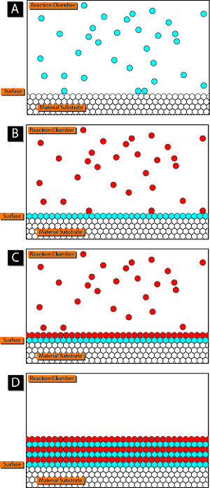
A basic schematic of the atomic layer deposition process. In Frame A, precursor 1 (in blue) is added to the reaction chamber containing the material surface to be coated ALD. After precursor 1 has adsorbed on the surface, any excess is removed from the reaction chamber. Precursor 2 (red) is added (Frame B) and reacts with precursor 1 to create another layer on the surface (Frame C). Precursor 2 is then cleared from the reaction chamber and this process is repeated until a desired thickness is achieved and the resulting product resembles Frame D.
 
Atomic layer deposition (ALD) is a thin-film deposition technique based on the sequential use of a gas phase chemical process. ALD is considered a subclass of chemical vapor deposition. The majority of ALD reactions use two chemicals, typically called precursors. These precursors react with the surface of a material one at a time in a sequential, self-limiting, manner. Through the repeated exposure to separate precursors, a thin film is slowly deposited. ALD is a key process in the fabrication of semiconductor devices, and part of the set of tools available for the synthesis of nanomaterials.

Introduction

Atomic layer deposition (ALD) is a thin-film deposition method in which a film is grown on a substrate by exposing its surface to alternate gaseous species (typically referred to as precursors). In contrast to chemical vapor deposition, the precursors are never present simultaneously in the reactor, but they are inserted as a series of sequential, non-overlapping pulses. In each of these pulses the precursor molecules react with the surface in a self-limiting way, so that the reaction terminates once all the reactive sites on the surface are consumed. Consequently, the maximum amount of material deposited on the surface after a single exposure to all of the precursors (a so-called ALD cycle) is determined by the nature of the precursor-surface interaction. By varying the number of cycles it is possible to grow materials uniformly and with high precision on arbitrarily complex and large substrates.

ALD is considered one deposition method with great potential for producing very thin, conformal films with control of the thickness and composition of the films possible at the atomic level. A major driving force for the recent interest is the prospective seen for ALD in scaling down microelectronic devices according to Moore's law. ALD is an active field of research, with hundreds of different processes published in the scientific literature, though some of them exhibit behaviors that depart from that of an ideal ALD process.

History

ALD has been developed in two independent discoveries under names atomic layer epitaxy (ALE, Finland) and molecular layering (ML, Soviet Union). To clarify the early history, an open effort called the Virtual Project on the History of ALD (VPHA) has been set up in summer 2013 by a group of scientists. Results from VPHA are dedicated essays that describe the historical development of ALD under the names ALE and ML; a review article that presents a short recommended reading list of early ALD publications up to 1986; and an article of learnings from the VPHA.

In the 1960s, Stanislav Ivanovich Koltsov together with Valentin Borisovich Aleskovskii and colleagues experimentally developed the principles of ALD at Leningrad (Lensovet) Technological Institute (LTI) in the Soviet Union. The purpose was to experimentally build upon the theoretical considerations of the "framework hypothesis" coined by Valentin Borisovich Aleskovskii in his doctor of science thesis ("professor's thesis") published in 1952. The experiments started with metal chloride reactions and water with porous silica, soon extending to other substrate materials and planar thin films. Aleskovskii and Koltsov together proposed the name "Molecular Layering" for the new technique in 1965. The principles of Molecular Layering were summarized in the doctoral thesis ("professor's thesis") of Koltsov in 1971. Research activities of molecular layering covered a broad scope, from fundamental chemistry research to applied research with porous catalysts, sorbents and fillers to microelectronics and beyond.

In 1974, when starting the development of thin-film electroluminescent displays (TFEL) at Instrumentarium Oy in Finland, Tuomo Suntola devised ALD as an advanced thin-film technology. Suntola named it atomic layer epitaxy (ALE) based on the meaning of "epitaxy" in Greek language, "arrangement upon". The first experiments were made with elemental Zn and S to grow ZnS. ALE as a means for growth of thin films was internationally patented in more than 20 countries. A breakthrough occurred, when Suntola and co-workers switched from high vacuum reactors to inert gas reactors which enabled the use of compound reactants like metal chlorides, hydrogen sulphide and water vapor for performing the ALE process. The technology was first disclosed in 1980 SID conference. The TFEL display prototype presented consisted of a ZnS layer between two aluminum oxide dielectric layers, all made in an ALE process using ZnCl2 + H2S and AlCl3 + H2O as the reactants. The first large-scale proof-of-concept of ALE-EL displays were the flight information boards installed in the Helsinki-Vantaa airport in 1983. TFEL flat panel display production started in the mid-1980s by Lohja Oy in the Olarinluoma factory. Academic research on ALE started in Tampere University of Technology (where Suntola gave lectures on electron physics) in 1970s, and in 1980s at Helsinki University of Technology. TFEL display manufacturing remained until the 1990s the only industrial application of ALE. In 1987, Suntola started the development of the ALE technology for new applications like photovoltaic devices and heterogeneous catalysts in Microchemistry Ltd., established for that purpose by the Finnish national oil company Neste Oy. In the 1990s, ALE development in Microchemistry was directed to semiconductor applications and ALE reactors suitable for silicon wafer processing. In 1999, Microchemistry Ltd. and the ALD technology were sold to the Dutch ASM International, a major supplier of semiconductor manufacturing equipment and Microchemistry Ltd. became ASM Microchemistry Oy as ASM's Finnish daughter company. Microchemistry Ltd/ASM Microchemistry Ltd was the only manufacturer of commercial ALD-reactors in the 1990s. In the early 2000s, the expertise on ALD reactors in Finland triggered two new manufacturers, Beneq Oy and Picosun Oy, the latter started by Sven Lindfors, Suntola's close coworker since 1975. The number of reactor manufacturers increased rapidly and semiconductor applications became the industrial breakthrough of the ALD technology, as ALD became an enabling technology for the continuation of Moore's law. In 2004, Tuomo Suntola received the European SEMI award for the development of the ALD technology for semiconductor applications and in 2018 the Millennium Technology Prize.

The developers of ML and ALE met at the 1st international conference on atomic layer epitaxy, "ALE-1" in Espoo, Finland, 1990. For some reason, knowledge of molecular layering in the growing English-speaking ALD community has remained marginal. An attempt to expose the extent of molecular layering works was made in a scientific ALD review article in 2005 and later in the VPHA-related publications.

The name "atomic layer deposition" was apparently proposed for the first time in writing as an alternative to ALE in analogy with CVD by Markku Leskelä (professor at the University of Helsinki) at the ALE-1 conference, Espoo, Finland. It took about a decade, before the name gained general acceptance with the onset of the international conference series on Atomic Layer Deposition by American Vacuum Society.

Surface reaction mechanisms

In a prototypical ALD process, a substrate is exposed to two reactants A and B in a sequential, non-overlapping way. In contrast to other techniques such as chemical vapor deposition (CVD), where thin-film growth proceeds on a steady-state fashion, in ALD each reactant reacts with the surface in a self-limited way: the reactant molecules can react only with a finite number of reactive sites on the surface. Once all those sites have been consumed in the reactor, the growth stops. The remaining reactant molecules are flushed away and only then reactant B is inserted into the reactor. By alternating exposures of A and B, a thin film is deposited. This process is shown in the side figure. Consequently, when describing an ALD process one refers to both dose times (the time a surface is being exposed to a precursor) and purge times (the time left in between doses for the precursor to evacuate the chamber) for each precursor. The dose-purge-dose-purge sequence of a binary ALD process constitutes an ALD cycle. Also, rather than using the concept of growth rate, ALD processes are described in terms of their growth per cycle.

In ALD, enough time must be allowed in each reaction step so that a full adsorption density can be achieved. When this happens the process has reached saturation. This time will depend on two key factors: the precursor pressure, and the sticking probability. Therefore, the rate of adsorption per unit of surface area can be expressed as:
Where R is the rate of adsorption, S is the sticking probability, and F is the incident molar flux.[15] However, a key characteristic of ALD is the S will change with time, as more molecules have reacted with the surface this sticking probability will become smaller until reaching a value of zero once saturation is reached. 

The specific details on the reaction mechanisms are strongly dependent on the particular ALD process. With hundreds of process available to deposit oxide, metals, nitrides, sulfides, chalcogenides, and fluoride materials, the unraveling of the mechanistic aspects of ALD processes is an active field of research. Some representative examples are shown below.

Thermal Al2O3 ALD

Among the different processes published in the literature, the synthesis of Al2O3 from trimethylaluminum (TMA) and water is one of the better known, and the self-limited growth of Al2O3 can be achieved in a wide range of temperature ranging from room temperature to more than 300 °C.

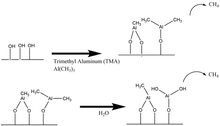
During the TMA exposure, TMA dissociatively chemisorbs on the substrate surface and any remaining TMA is pumped out of the chamber. The dissociative chemisorption of TMA leaves a surface covered with AlCH3. The surface is then exposed to H2O vapor, which reacts with the surface –CH3 forming CH4 as a reaction byproduct and resulting on a hydroxylated Al2O3 surface.

Proposed Mechanism for Al2O3 ALD during the a) TMA reaction b) H2O reaction

Metal ALD

Metal ALD via elimination reactions most commonly occurs when metals functionalized with halogens (i.e. metal fluorides) are reacted with silicon precursors. Common metals deposited using fluorosilane elimination reactions are tungsten and molybdenum because the respective elimination reactions for these metals are highly exothermic For Tungsten ALD, Si–H and W–F entities exist on the material's surface prior to the final purging process, and a linear deposition rate of W has been observed per each AB reactant cycle. Typical growth rates per cycle for Tungsten ALD are 4 to 7 Angstroms and typical reaction temperatures are 177 °C to 325 °C. Two surface reactions, as well as an overall ALD reaction for tungsten ALD, are presented below. A multitude of other metals can be deposited by ALD via the reactions below if their reaction sequences are based on fluorosilane elimination.
Primary Reactions at Surface:
WSiF2H* + WF6--> WWF5* + SiF3H (7)
WF5* + Si2H6 --> WSiF2H* + SiF3H + 2H2 (8)
Overall ALD Reaction:
WF6 + Si2H6 --> W + 2SiF3H + 2H2 ∆H = -181kcal (9)

Catalytic SiO2 ALD

The use of catalysts is of paramount importance in delivering reliable methods of SiO2 ALD. Without catalysts, surface reactions leading to the formation of SiO2 are generally very slow and only occur at exceptionally high temperatures. Typical catalysts for SiO2 ALD include Lewis bases such as NH3 or pyridine and SiO2 ; ALD can also be initiated when these Lewis bases are coupled with other silicon precursors such as tetraethoxysilane (TEOS). Hydrogen bonding is believed to occur between the Lewis base and the SiOH* surface species or between the H2O based reactant and the Lewis base. Oxygen becomes a stronger nucleophile when the Lewis base hydrogen bonds with the SiOH* surface species because the SiO-H bond is effectively weakened. As such, the electropositive Si atom in the SiCl4 reactant is more susceptible to nucleophilic attack. Similarly, hydrogen bonding between a Lewis base and an H2O reactant make the electronegative O in H2O a strong nucleophile that is able to attack the Si in an existing SiCl* surface species. The use of a Lewis base catalyst is more or less a requirement for SiO2 ALD, as without a Lewis base catalyst, reaction temperatures must exceed 325 °C and pressures must exceed 103 torr. Generally, the most favorable temperature to perform SiO2 ALD is at 32 °C and a common deposition rate is 1.35 Angstroms per binary reaction sequence. Two surface reactions for SiO2 ALD, an overall reaction, and a schematic illustrating Lewis base catalysis in SiO2 ALD are provided below.
Primary Reactions at Surface:
SiOH* + SiCl4--> SiOSiCl3* + HCl (4)
SiCl* + H2O --> SiOH* + HCl (5)
Overall ALD Reaction:
SiCl4 + 2H2O --> SiO2 + 4HCl (6)
Proposed Mechanism of Lewis base catalysis of SiO2 ALD during a) an SiCl4 reaction and b) an H2O reaction
 
ALD Reaction Mechanisms Summary Table
Type of ALD Temperature range Viable precursors Reactants Applications
Catalytic ALD >32 °C with Lewis Base Catalyst Metal oxides (i.e. TiO2, ZrO2,SnO22) (Metal)Cl4, H2O High k-dielectric layers, protective layers, anti-reflective layers, etc.
Al2O3 ALD 30–300 °C Al2O3, metal oxides (Metal)Cl4, H2O, Ti(OiPr)4,
(Metal)(Et)2
Dielectric layers, insulating layers, etc., Solar Cell surface passivations
Metal ALD Using Thermal Chemistry 175–400 °C Metal Fluorides, organometallics, catalytic metals M(C5H5)2, (CH3C5H4)M(CH3)3 ,
Cu(thd)2, Pd(hfac)2,
Ni(acac)2, H2
Conductive pathways, catalytic surfaces, MOS devices
ALD on polymers 25–100 °C Common polymers (Polyethylene, PMMA, PP, PS, PVC, PVA, etc.) Al(CH3)3, H2O, M(CH3)3 Polymer surface functionalization, creation of composites, diffusion barriers, etc.
ALD on particles Varies: 25–100 deg C for polymer particles, 100–400 deg C for metal/alloy particles BN, ZrO2, CNTs, polymer particles Various gases:
Fluidized bed reactors are used
to allow coating of
individual particles
Deposition of protective and insulative coatings, optical and mechanical property modification, formation of composite structures, conductive mediums
Plasma or Radical-enhanced ALD for single element ALD materials 20–800 °C Pure metals (i.e. Ta, Ti, Si, Ge, Ru, Pt), metal nitrides (i.e. TiN, TaN, etc.) Organometallics, MH2Cl2, tertbutylimidotris(diethylamido)
tantalum (TBTDET), bis(ethylcyclopentadienyl)
ruthenium), NH3
DRAM structures, MOSFET and semiconductor devices, capacitors
Plasma Enhanced ALD of Metal Oxides and Nitrides 20–300 °C Al2O3, SiO2, ZnOx, InOx, HfO2, SiNx, TaNx similar to thermal ALD

Applications

ALD can be used for a great deal of applications. Some of the main fields that ALD is used for are microelectronics and biomedical applications. Details about these applications are outlined in the following sections.

Microelectronics applications

ALD is a useful process for the fabrication of microelectronics due to its ability to produce accurate thicknesses and uniform surfaces in addition to high quality film production using various different materials. In microelectronics, ALD is studied as a potential technique to deposit high-κ (high permittivity) gate oxides, high-κ memory capacitor dielectrics, ferroelectrics, and metals and nitrides for electrodes and interconnects. In high-κ gate oxides, where the control of ultra thin films is essential, ALD is only likely to come into wider use at the 45 nm technology. In metallizations, conformal films are required; currently it is expected that ALD will be used in mainstream production at the 65 nm node. In dynamic random access memories (DRAMs), the conformality requirements are even higher and ALD is the only method that can be used when feature sizes become smaller than 100 nm. Several products that use ALD include magnetic recording heads, MOSFET gate stacks, DRAM capacitors, nonvolatile ferroelectric memories, and many others.

Gate oxides

Deposition of the high-κ oxides Al2O3, ZrO2, and HfO2 has been one of the most widely examined areas of ALD. The motivation for high-κ oxides comes from the problem of high tunneling current through the commonly used SiO2 gate dielectric in metal-oxide-semiconductor field-effect transistors (MOSFETs) when it is downscaled to a thickness of 1.0 nm and below. With the high-κ oxide, a thicker gate dielectric can be made for the required capacitance density, thus the tunneling current can be reduced through the structure.

Intel Corporation has reported using ALD to deposit high-κ gate dielectric for its 45 nm CMOS technology.

Transition-metal nitrides

Transition-metal nitrides, such as TiN and TaN find potential use both as metal barriers and as gate metals. Metal barriers are used in modern Cu-based chips to avoid diffusion of Cu into the surrounding materials, such as insulators and the silicon substrate, and also, to prevent Cu contamination by elements diffusing from the insulators by surrounding every Cu interconnection with a layer of metal barriers. The metal barriers have strict demands: they should be pure; dense; conductive; conformal; thin; have good adhesion towards metals and insulators. The requirements concerning process technique can be fulfilled by ALD. The most studied ALD nitride is TiN which is deposited from TiCl4 and NH3.

Metal films

Motivations of an interest in metal ALD are:
  1. Cu interconnects and W plugs, or at least Cu seed layers for Cu electrodeposition and W seeds for W CVD,
  2. transition-metal nitrides (e.g. TiN, TaN, WN) for Cu interconnect barriers
  3. noble metals for ferroelectric random access memory (FRAM) and DRAM capacitor electrodes
  4. high- and low-work function metals for dual-gate MOSFETs.

Magnetic recording heads

Magnetic recording heads utilize electric fields to polarize particles and leave a magnetized pattern on a hard disk. Al2O3 ALD is used to create uniform, thin layers of insulation. By using ALD, it is possible to control the insulation thickness to a high level of accuracy. This allows for more accurate patterns of magnetized particles and thus higher quality recordings.

DRAM capacitors

Dynamic random-access memory (DRAM) capacitors are yet another application of ALD. An individual DRAM cell can store a single bit of data and consists of a single MOS transistor and a capacitor. Major efforts are being put into reducing the size of the capacitor which will effectively allow for greater memory density. In order to change the capacitor size without affecting the capacitance, different cell orientations are being used. Some of these include stacked or trench capacitors. With the emergence of trench capacitors, the problem of fabricating these capacitors comes into play, especially as the size of semiconductors decreases. ALD allows trench features to be scaled to beyond 100 nm. The ability to deposit single layers of material allows for a great deal of control over the material. Except for some issues of incomplete film growth (largely due to insufficient amount or low temperature substrates), ALD provides an effective means of depositing thin films like dielectrics or barriers.

Biomedical applications

Understanding and being able to specify the surface properties on biomedical devices is critical in the biomedical industry, especially regarding devices that are implanted in the body. A material interacts with the environment at its surface, so the surface properties largely direct the interactions of the material with its environment. Surface chemistry and surface topography affect protein adsorption, cellular interactions, and the immune response.

Some current uses in biomedical applications include creating flexible sensors, modifying nanoporous membranes, polymer ALD, and creating thin biocompatible coatings. ALD has been used to deposit TiO2 films to create optical waveguide sensors as diagnostic tools. Also, ALD is beneficial in creating flexible sensing devices that can be used, for example, in the clothing of athletes to detect movement or heart rate. ALD is one possible manufacturing process for flexible organic field-effect transistors (OFETs) because it is a low-temperature deposition method.

Nanoporous materials are emerging throughout the biomedical industry in drug delivery, implants, and tissue engineering. The benefit of using ALD to modify the surfaces of nanoporous materials is that, unlike many other methods, the saturation and self-limiting nature of the reactions means that even deeply embedded surfaces and interfaces are coated with a uniform film. Nanoporous surfaces can have their pore size reduced further in the ALD process because the conformal coating will completely coat the insides of the pores. This reduction in pore size may be advantageous in certain applications.

Quality and quality control

The quality of an ALD process can be monitored using several different imaging techniques to make sure that the ALD process is occurring smoothly and producing a conformal layer over a surface. One option is cross-sectional SEM images or transmission electron microscopy (TEM) images, which allow for inspection at the micro and nano scale. High magnification of images is pertinent for assessing the quality of an ALD layer. XRR, or X-ray reflectivity, is a technique that measures thin-film properties including thickness, density, and surface roughness. Another optical quality evaluation tool is spectroscopic ellipsometry (SE). Using SE in between the depositions of each layer added on by ALD provides information on the growth rate and material characteristics of the film can be assessed.

Applying this analysis tool during the ALD process, sometimes referred to as in situ spectroscopic ellipsometry, allows for greater control over the growth rate of the films during the ALD process. This type of quality control occurs during the ALD process rather than assessing the films afterwards as in TEM imaging, or XRR. Additionally, Rutherford backscattering spectroscopy (RBS), X-Ray photoelectron spectroscopy (XPS), Auger electron spectroscopy (AES), and four-point probe (FPP) are some other techniques that can be used to provide quality control information with regards to thin films deposited by ALD.

Advantages and limitations

Advantages

ALD provides a very controlled method to produce a film to an atomically specified thickness. Also, the growth of different multilayer structures is straightforward. Due to the sensitivity and precision of the equipment, it is very beneficial to those in the field of microelectronics and nanotechnology in producing small, but efficient semiconductors. ALD is typically run at lower temperatures along with a catalyst which is thermochemically favored. The lower temperature is beneficial when working with fragile substrates, such as biological samples. Some precursors that are thermally unstable still may be used so long as their decomposition rate is relatively slow.

Disadvantages

High purity of the substrates is very important, and as such, high costs will ensue (Stanford). Although this cost may not be much relative to the cost of the equipment needed, one may need to run several trials before finding conditions that favor their desired product. Once the layer has been made and the process is complete, there may be a requirement of needing to remove excess precursors from the final product. In some final products there are less than one percent of impurities present.

Economic viability

Atomic layer deposition instruments can range anywhere from $200,000 to $800,000 based on the quality and efficiency of the instrument. There is no set cost for running a cycle of these instruments; the cost varies depending on the quality and purity of the substrates used, as well as the temperature and time of machine operation. Some substrates are less available than others and require special conditions, as some are very sensitive to oxygen and may then increase the rate of decomposition. Multicomponent oxides and certain metals traditionally needed in the microelectronics industry are generally not cost efficient.

Reaction time

The process of ALD is very slow and this is known to be its major limitation. For example, Al2O3 is deposited at a rate of 0.11 nm per cycle, which can correspond to an average deposition rate of 100–300 nm per hour, depending on cycle duration and pumping speed. ALD is typically used to produce substrates for microelectronics and nanotechnology, and therefore, thick atomic layers are not needed. Many substrates cannot be used because of their fragility or impurity. Impurities are typically found on the 0.1-1% atomic level because of some of the carrier gases are known to leave residue and are also sensitive to oxygen.

Chemical limitations

Precursors must be volatile, but not subject to decomposition, as most precursors are very sensitive to oxygen/air, thus causing a limitation on the substrates that may be used. Some biological substrates are very sensitive to heat and may have fast decomposition rates that are not favored and yield larger impurity levels. There are a multitude of thin-film substrate materials available, but the important substrates needed for use in microelectronics can be hard to obtain and may be very expensive.

Finally, Fusion Power Is About to Become a Reality

Long considered a joke, or a pipe dream, fusion is suddenly making enormous leaps.

The idea first lit up Dennis Whyte when he was in high school, in the remote reaches of Saskatchewan, Canada, in the 1980s. He wrote a term paper on how scientists were trying to harness fusion (the physical effect that fuels the stars) in wondrously efficient power plants on Earth. This is the ultimate clean-energy dream. It would provide massive amounts of clean electricity, with no greenhouse gases or air pollution. It would do it on a constant basis, unlike solar and wind. Whatever waste it created would be easily manageable, unlike today’s nuclear power plants. And fuel would be limitless. One of the main ingredients needed for fusion is abundant in water. Just one little gram of hydrogen fuel for a fusion reactor would provide as much power as 10 tons of coal.

Whyte got an A on that paper, but his physics teacher also wrote: “It’s too complicated.” That comment, Whyte says with a hearty laugh, “was sort of a harbinger of things to come.”

Indeed, over the next few decades, as Whyte mastered the finicky physics that fusion power would require and became a professor at MIT, the concept seemingly got no closer to becoming reality. It’s not that the science was shaky: It’s that reliably bottling up miniature stars, inside complex machines on Earth, demands otherworldly amounts of patience, not to mention billions and billions of dollars. Researchers, like Whyte, knew all too well the sardonic joke about their work: fusion is the energy source of the future, and it always will be.

That line took on an especially bitter edge one day in 2012, when the U.S. Department of Energy announced it would eliminate funding for MIT’s experimental fusion reactor. Whyte was angry about the suddenness of the news. “It was absolutely absurd — you can put that in your article — fucking absurd that happened with a program that was acknowledged to be excellent.” But above all, he was dismayed. Global warming was bearing down year after year, yet this idea that could save civilization was losing what little momentum it had.
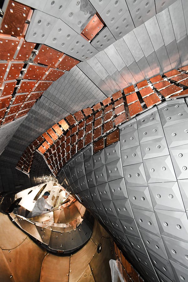
Wendelstein 7-X fusion reactor in Germany, 2017. Photo: Picture Alliance/Getty

So Whyte thought about giving up. He looked for other things to focus on, “stuff that wasn’t as exciting, quite frankly,” but stuff that would be achievable. “Everyone understands delays in projects, and science hurdles you’ve got to overcome, but I saw fusion energy being used for something accelerating away from us,” he says. “You start getting pretty dejected when you realize, in your professional career, you’re never going to see this happen.”

As it turned out, Whyte never really walked away. Instead, he and his colleagues and graduate students at MIT’s Plasma Science and Fusion Center figured out a new angle. And last winter, MIT declared that Whyte’s lab had a fundamentally new approach to fusion and threw its weight behind their plan with an unusually public bet, spinning out a company to capitalize on it. An Italian oil company and private investors — including a firm funded by Bill Gates and Jeff Bezos — put at least $75 million into the company, known as Commonwealth Fusion Systems [CFS]. The startup intends to demonstrate the workings of fusion power by 2025.
The recent progress is remarkable, says the founder of one startup developing fusion power. “The world has been waiting for fusion for a long time.”
Real, live, economically viable power plants could then follow in the 2030s. No joke. When I ask Whyte, who is 54, to compare his level of optimism now to any other point in his career, he says, simply: “It is at the maximum.”

But it’s not just MIT. At least 10 other startups also are trying new approaches to fusion power. All of them contend that it’s no longer a tantalizingly tricky science experiment, and is becoming a matter of engineering. If even just one of these ventures can pull it off, the energy source of the future is closer than it seems.

“It’s remarkable,” says David Kingham, executive vice chairman of Tokamak Energy, a British company whose goal is to put fusion power on the grid by 2030. “The world has been waiting for fusion for a long time.”


Imagine that I told you I was developing a special machine. If I put power into it, I could get 10 times as much out. Because of the undeniable laws of physics, I could show you on paper exactly why it should be a cost-effective source of vast amounts of electricity.

Oh, here’s the catch: My paper sketch would come true — especially the part about it being cost-effective — but only if I built the machine just right. Which might require materials that haven’t been invented yet. Until I perfected that design, my machine would use up more power than it produced. 

And I couldn’t get close to perfecting the design without spending years and years building expensive test machines that would reveal problems that I would try to address in subsequent versions.

If it seems crazy, well, that’s the story of fusion power.

Fusion definitely works. You see it every day. Our sun and other stars blast hydrogen atoms together with such intense force that their nuclei overcome their normal inclination to repel each other. Instead they fuse, sparking a reaction that transforms the hydrogen into helium and releases cosmic amounts of energy in the process.

We also have great paper sketches for fusion power machines. Fusion happens inside stars because of the crushing pressure created by their gravity. To generate that effect inside a fusion reactor, ionized gas — which is called plasma — must be heated and compressed by man-made forces, such as an ultra-powerful magnetic field. But whatever the method, there’s just one main goal. If you get enough plasma to stay hot enough for long enough, then you can trigger so much fusion inside it that a huge multiplier effect is unlocked. At that point, the energy that is released helps keep the plasma hot, extending the reaction. And there still is plenty of energy left over to turn into electricity.

The problem is that we’re still plugging away on predecessors to the machines that could generate that effect. Ever since the 1950s, scientists have used spherical or doughnut-shaped machines called tokamaks, including the one at MIT that lost funding a few years ago, to create fusion reactions in plasmas bottled up by magnetic fields. But no one has done it long enough — while also getting it hot enough and dense enough — to really tip the balance and get it going. Heating the plasma and squeezing it in place still takes more energy than you can harvest from it.

So, that’s the name of the game in fusion: to get past that point. ITER, a mega-billion-dollar reactor being built in France by an international consortium, is designed to do it and finally prove the concept. But ITER — which is also way behind schedule and over budget — overcomes the limitations of previous tokamaks by being enormous. It’s the size of 60 soccer fields, which probably isn’t an economical setup for power plants that the world will need by the tens of thousands.
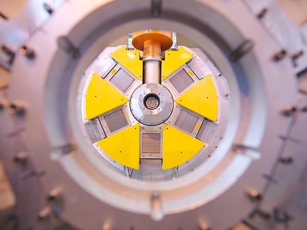
ITER (International Thermonuclear Experimental Reactor) under construction. Photo: Christophe Simon/Getty

Could you go the other direct ion, and instead make fusion machines much smaller, which is also to say much less expensive? That is what motivates all the fusion startups. Several have decided the answer is to use something other than a tokamak and its circular coils of magnets. They’re updating old designs, including hitting plasma with lasers, or cooking up new ones, such as compressing it with something like a particle accelerator. One startup plans to push on the material with pistons.

But Whyte and his colleagues at MIT made a different decision, one that could prove crucial to making fusion power arise sooner than people expect. Even though things looked dire a few years ago, when their fusion machine lost funding, Whyte’s team decided to double down on tokamaks. As Whyte saw it, why try to invent something totally new when you could take advantage of all those decades and billions spent researching tokamaks? Instead, they would rethink the design to make tokamaks modular and much cheaper and weave in brand-new materials that can induce and confine a fusion reaction.

After getting the news of the funding shutdown, the university, and other supporters of the program, persuaded Congress to grant a temporary reprieve. They could keep running their fusion reactor into 2016, enough time for experiments to be finished and to keep PhD students going on the research they had come to MIT to undertake. And then they dug in.


The most intriguing questions Whyte and his students were exploring had to do with how tokamaks could produce lots of electricity without being gigantic and expensive. MIT’s tokamak, which still sits in a two-story tall, garage-like room in a former Nabisco cookie warehouse, generated a magnetic field by running electricity through copper coils that surrounded a round metal chamber. In that chamber, plasma would be heated with microwaves and other methods to millions of degrees. On one of its last runs, it set a new record for plasma pressure while hitting 35 million Celsius.

Just outside the chamber, the vital measurement isn’t heat, but cold. The magnets that squeeze the plasma in place have to be kept well below minus-200 Celsius, or else their performance will degrade from a buildup of electrical resistance.
Particle accelerator. Photo: Monty Rakusen/Getty

It was a graduate student who suggested that the MIT team see what would happen if they made magnets out of a newly developed superconducting tape. A superconductor conducts electricity so well that it doesn’t build up electrical resistance and this new tape maintains that property, even at slightly higher temperatures than other superconductors do.

Using less energy on cooling could make a tokamak cheaper to run. But that benefit was minor compared to the other things Whyte’s group figured out. As they plotted out ways of winding the tape into coils in a tokamak, they realized this method could double the strength of the magnetic field they could exert on a plasma. Increasing the field strength is crucial because plasma is wild. It’s unstable and evasive, and only overwhelming force can keep it from spreading out and cooling too much.

Perhaps best of all: using this tape instead of rigid superconductors could make the machine 10 times smaller.

That led them to another problem with traditional tokamaks. If you need to replace parts of the machine, you have to take the whole thing apart and put it back together. That’s unacceptable for a power plant in regular use. And again, one of Whyte’s graduate students had a great idea. If you apply the superconducting tape in sections, with joints, the magnets can be snapped on and off for quick and easy repairs or upgrades.

“This was the beginning of the ‘aha!’ moment,” Whyte says. “The people who are in CFS were in that class.”

Other big ideas kept coming. One of the great things about fusion is its inherent safety. It’s impossible for this tiny star to slip out and cause trouble, because the plasma’s weird physical state can’t be sustained outside of the magnetic field. Still, the plasma does send something out that you’ve got to deal with: neutrons.

Fusion projects generally aim to fuse two forms of hydrogen: deuterium and tritium. Deuterium is readily available in seawater, but tritium is very rare, so you have to make it. (More on that in a minute.) In this version of fusion, 80 percent of the energy that is released comes out in the form of neutrons. These are subatomic particles that have no electric charge, so they’re not contained by the magnetic field. They come flying out like angry spittle.

In fusion experiments measured in seconds or less, flying neutrons aren’t a big problem. But over time, they can be nasty. These particles jump a foot and a half from the plasma and have enough energy to rearrange the atoms in the tokamak’s inner wall, eventually degrading it. What to do about that in a power plant that needs to run for long stretches?

Whyte describes the answer with a wry smile. “We turned the problem around,” he says.

In essence, the MIT plan takes a ride on the neutrons by catching them in a liquid. Neutrons wreck solid materials by scrambling the order of their atoms, but liquids are already disordered, by definition. In the design that CFS is developing, the neutrons pass through an inch or two of steel and then barrel into a liquified salt, which they essentially just heat up. Then, that molten salt can be pumped around a power station to generate electricity. By the way, there’s lithium in the molten salt, and when neutrons hit lithium, they create tritium, which you can take out and use to fuel the fusion reactor.

Thetatron Experiment designed to study the ionisation and compression produced in deuterium plasma, 1964. Photo: Fox Photos/Getty

This setup isn’t perfect, however. Blanketing the tokamak’s steel wall with molten salt will lessen, but not eliminate, the damage that the neutrons would otherwise cause to the metal. It will have to be replaced every so often. Just how often? That’s a crucial question for the cost of a power plant.

For now, Whyte says, the metal barrier should last a year or two. That’s not great, so materials that better withstand neutrons have to be developed, to extend the lifespan of that wall. That looks doable; reducing the erosion of the wall in fusion reactors is a long-standing field of research.

But the issue is nonetheless significant enough that General Fusion, the company that intends to compress plasma with pistons, plans to keep a solid metal case relatively far away. It will directly surround the plasma with liquid metal that gets pumped off to convert its heat to electricity. There will be lithium in that liquid, too, to breed tritium.

Even if the MIT team manages to extend the life of the barrier, there’s another issue: The neutron bombardment will eventually render the metal radioactive.

Is that a big problem? Well, one of the novel things about a fusion company called TAE Technologies, which has raised $600 million from Google, the late Microsoft founder Paul Allen, and other luminaries, is that it plans to fuse hydrogen protons with boron, a reasonably abundant element, because that reaction emits hardly any neutrons. TAE’s co-founder and CEO, Michl Binderbauer, says that because of its cleaner profile, hydrogen-boron fusion is “the single shining opportunity for mankind.”

But since we’re talking about fusion, of course there’s a catch. Hydrogen-boron fusion is much harder to pull off: The plasma has to get to billions of degrees, not millions. And the “reaction rate” is much lower, which means less fusion happens. TAE is going to start with deuterium-tritium fusion before trying to work its way up.

In the meantime, Whyte and just about everyone else in fusion thinks deuterium-tritium fusion is well worth gunning for. Any radioactive components in MIT’s design will be relatively small and have a short half-life. The material would be nowhere near as problematic as the stuff that comes out of nuclear power plants today. If fusion plant operators have to replace the inner wall from the reactor Whyte envisions, they’d “put it in a swimming pool for 10 years,” he says. “And then you can walk up beside it.”


Before any of that happens, CFS will try to pull off fusion’s most elusive trick: doing something ahead of schedule.

With the investment it’s raised, the company has about three years to test components of its reactor design, especially those still-unproven new magnets. Then, it will need to raise hundreds of millions to build a prototype reactor, at a location to be determined. The company has said it intends to get that reactor running by 2025. But its CEO, a former MIT graduate student named Robert Mumgaard, says it could happen even sooner.

Alas, fusion timelines still have a habit of slipping, even in private companies. Over the past few years, the defense contractor Lockheed Martin, and a few startups, said they hoped to show working prototypes by now — possibly even ones that achieved the ultimate, a net power gain. That hasn’t happened. When I asked for updates, I got some vague replies, ranging from “we are hard at work” to “the preliminary results are promising.”
If fusion power just won’t work, “I’m scared for the world,” says the CEO of Commonwealth Fusion Systems.
I got the most reassuring answer from Christofer Mowry, CEO of General Fusion.

His company said in 2017 that it hoped to get its first prototype running in three to five years. It’s really more like five years from now. But, he says, that’s because the company has needed time to raise “a few hundred million dollars,” not because fusion science is still iffy. Because so many companies are trying to make fusion power practical, and because demand for it will be so high, “I’m 100 percent confident that this is going to happen,” Mowry says. “Are we going to have commercial fusion power plants on the grid by 2030? Maybe. But it won’t be 50 years, I can tell you that.”

At CFS, Mumgaard sees parallels with the story of human flight. Before the Wright brothers finally got a plane off the ground, a lot of people tried and got kind of close. Plenty of observers assumed that meant human flight would always remain a fantasy. But all that time, through all those failures with gliders and flapping man-made wings, engineers were systematically probing aerodynamics. The Wright brothers built on that knowledge and combined it with insights about control mechanisms that they had from working with bicycles. And only then, was it obvious: yes, humans can fly.

“When you have the insight into a piece of technology and you get it over that hump, it goes,” Mumgaard says. “We’re think we’re at this point.” He refers to his company’s plan to build a prototype as the Kitty Hawk moment.

But what if that parallel breaks down? What if fusion power just won’t work, or won’t work at a cost that anyone will be willing to pay? Then “I’m scared for the world,” Mumgaard says.

And it’s hard to cheer him up on that point. None of the existing carbon-free alternatives seem suited to the scale of the climate problem. Conventional nuclear power is unpopular and expensive. There aren’t many more waterways to dam. For solar and wind to be the primary answer, you’d need epic amounts of batteries, which might be environmentally or economically prohibitive.

When I pose the same question to Whyte, I get a slightly different answer. He sounds like a person who has considered what would happen if he gave up on this dream, and then renewed it instead. “I would never say ‘if we don’t develop fusion we’re not going to make it,’” he says. “But, boy, I’ll put it the other way around: If you make fusion economical, you have given yourself an arrow in the quiver which is almost unmatched in going after this.”

“We’re giving it our best shot,” he continues. “Others are giving it their best shot.” And then he slaps his hand on the table in front of him for emphasis. “Let’s get there.”

Introduction to entropy

From Wikipedia, the free encyclopedia https://en.wikipedia.org/wiki/Introduct...