,
An image-forming optical system with aberration will produce an image which is not sharp. Makers of optical instruments need to correct optical systems to compensate for aberration.
Aberration can be analyzed with the techniques of geometrical optics. The articles on reflection, refraction and caustics discuss the general features of reflected and refracted rays.
Overview
Reflection
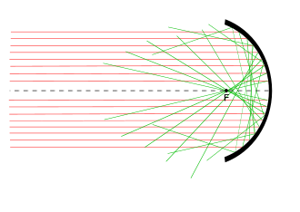
from a spherical mirror. Incident rays (red) away from the center of
the mirror produce reflected rays (green) that miss the focal point, F.
This is due to spherical aberration.
With an ideal lens, light from any given point on an object would pass through the lens and come together at a single point in the image plane (or, more generally, the image surface). Real lenses do not focus light exactly to a single point, however, even when they are perfectly made. These deviations from the idealized lens performance are called aberrations of the lens.
Aberrations fall into two classes: monochromatic and chromatic. Monochromatic aberrations are caused by the geometry of the lens or mirror and occur both when light is reflected and when it is refracted. They appear even when using monochromatic light, hence the name.
Chromatic aberrations are caused by dispersion, the variation of a lens's refractive index with wavelength. Because of dispersion, different wavelengths of light come to focus at different points. Chromatic aberration does not appear when monochromatic light is used.
Monochromatic aberrations
The most common monochromatic aberrations are:Although defocus is technically the lowest-order of the optical aberrations, it is usually not considered as a lens aberration, since it can be corrected by moving the lens (or the image plane) to bring the image plane to the optical focus of the lens.
In addition to these aberrations, piston and tilt are effects which shift the position of the focal point. Piston and tilt are not true optical aberrations, since when an otherwise perfect wavefront is altered by piston and tilt, it will still form a perfect, aberration-free image, only shifted to a different position.
Chromatic aberrations
Chromatic aberration occurs when different wavelengths are not focussed to the same point. Types of chromatic aberration are:- Axial (or "longitudinal") chromatic aberration
- Lateral (or "transverse") chromatic aberration
Theory of monochromatic aberration
A perfect optical system would follow the theorem: Rays of light proceeding from any object point unite in an image point; and therefore the object space is reproduced in an image space. The introduction of simple auxiliary terms, due to Gauss, named the focal lengths and focal planes, permits the determination of the image of any object for any system. The Gaussian theory, however, is only true so long as the angles made by all rays with the optical axis (the symmetrical axis of the system) are infinitely small, i.e. with infinitesimal objects, images and lenses; in practice these conditions may not be realized, and the images projected by uncorrected systems are, in general, ill-defined and often completely blurred, if the aperture or field of view exceeds certain limits.The investigations of James Clerk Maxwell and Ernst Abbe showed that the properties of these reproductions, i.e. the relative position and magnitude of the images, are not special properties of optical systems, but necessary consequences of the supposition (per Abbe) of the reproduction of all points of a space in image points, and are independent of the manner in which the reproduction is effected. These authors showed, however, that no optical system can justify these suppositions, since they are contradictory to the fundamental laws of reflection and refraction. Consequently, the Gaussian theory only supplies a convenient method of approximating to reality; and actual optical systems can only attempt to realize this unattainable ideal. At present, all that can be attempted is to reproduce a single plane in another plane; but even this has not been altogether satisfactorily accomplished: aberrations always occur, and it is improbable that these will ever be entirely corrected.
The classical theory of optics and related systems been analyzed by numerous authors.
Aberration of axial points (spherical aberration in the restricted sense)
Let S (fig. 1) be any optical system, rays proceeding from an axis point O under an angle u1 will unite in the axis point O'1; and those under an angle u2 in the axis point O'2. If there is refraction at a collective spherical surface, or through a thin positive lens, O'2 will lie in front of O'1 so long as the angle u2 is greater than u1 (under correction); and conversely with a dispersive surface or lenses (over correction). The caustic, in the first case, resembles the sign > (greater than); in the second < (less than). If the angle u1 is very small, O'1 is the Gaussian image; and O'1 O'2 is termed the longitudinal aberration, and O'1R the lateral aberration of the pencils with aperture u2. If the pencil with the angle u2 is that of the maximum aberration of all the pencils transmitted, then in a plane perpendicular to the axis at O'1 there is a circular disk of confusion of radius O'1R, and in a parallel plane at O'2 another one of radius O'2R2; between these two is situated the disk of least confusion.
The largest opening of the pencils, which take part in the reproduction of O, i.e. the angle u, is generally determined by the margin of one of the lenses or by a hole in a thin plate placed between, before, or behind the lenses of the system. This hole is termed the stop or diaphragm; Abbe used the term aperture stop for both the hole and the limiting margin of the lens. The component S1 of the system, situated between the aperture stop and the object O, projects an image of the diaphragm, termed by Abbe the entrance pupil; the exit pupil is the image formed by the component S2, which is placed behind the aperture stop. All rays which issue from O and pass through the aperture stop also pass through the entrance and exit pupils, since these are images of the aperture stop. Since the maximum aperture of the pencils issuing from O is the angle u subtended by the entrance pupil at this point, the magnitude of the aberration will be determined by the position and diameter of the entrance pupil. If the system be entirely behind the aperture stop, then this is itself the entrance pupil (front stop); if entirely in front, it is the exit pupil (back stop).
If the object point be infinitely distant, all rays received by the first member of the system are parallel, and their intersections, after traversing the system, vary according to their perpendicular height of incidence, i.e. their distance from the axis. This distance replaces the angle u in the preceding considerations; and the aperture, i.e. the radius of the entrance pupil, is its maximum value.
Aberration of elements, i.e. smallest objects at right angles to the axis
If rays issuing from O (fig. 1) are concurrent, it does not follow that points in a portion of a plane perpendicular at O to the axis will be also concurrent, even if the part of the plane be very small. As the diameter of the lens increases (i.e., with increasing aperture_, the neighboring point N will be reproduced, but attended by aberrations comparable in magnitude to ON. These aberrations are avoided if, according to Abbe, the sine condition, sin u'1/sin u1=sin u'2/sin u2, holds for all rays reproducing the point O. If the object point O is infinitely distant, u1 and u2 are to be replaced by h1 and h2, the perpendicular heights of incidence; the sine condition then becomes sin u'1/h1=sin u'2/h2. A system fulfilling this condition and free from spherical aberration is called aplanatic (Greek a-, privative, plann, a wandering). This word was first used by Robert Blair to characterize a superior achromatism, and, subsequently, by many writers to denote freedom from spherical aberration as well.Since the aberration increases with the distance of the ray from the center of the lens, the aberration increases as the lens diameter increases (or, correspondingly, with the diameter of the aperture), and hence can be minimized by reducing the aperture, at the cost of also reducing the amount of light reaching the image plane.
Aberration of lateral object points (points beyond the axis) with narrow pencils. Astigmatism.

Figure 2
A point O (fig. 2) at a finite distance from the axis (or with an infinitely distant object, a point which subtends a finite angle at the system) is, in general, even then not sharply reproduced if the pencil of rays issuing from it and traversing the system is made infinitely narrow by reducing the aperture stop; such a pencil consists of the rays which can pass from the object point through the now infinitely small entrance pupil. It is seen (ignoring exceptional cases) that the pencil does not meet the refracting or reflecting surface at right angles; therefore it is astigmatic (Gr. a-, privative, stigmia, a point). Naming the central ray passing through the entrance pupil the axis of the pencil or principal ray, it can be said: the rays of the pencil intersect, not in one point, but in two focal lines, which can be assumed to be at right angles to the principal ray; of these, one lies in the plane containing the principal ray and the axis of the system, i.e. in the first principal section or meridional section, and the other at right angles to it, i.e. in the second principal section or sagittal section. We receive, therefore, in no single intercepting plane behind the system, as, for example, a focusing screen, an image of the object point; on the other hand, in each of two planes lines O' and O" are separately formed (in neighboring planes ellipses are formed), and in a plane between O' and O" a circle of least confusion. The interval O'O", termed the astigmatic difference, increases, in general, with the angle W made by the principal ray OP with the axis of the system, i.e. with the field of view. Two astigmatic image surfaces correspond to one object plane; and these are in contact at the axis point; on the one lie the focal lines of the first kind, on the other those of the second. Systems in which the two astigmatic surfaces coincide are termed anastigmatic or stigmatic.
Sir Isaac Newton was probably the discoverer of astigmation; the position of the astigmatic image lines was determined by Thomas Young; and the theory was developed by Allvar Gullstrand. A bibliography by P. Culmann is given in Moritz von Rohr's Die Bilderzeugung in optischen Instrumenten.
Aberration of lateral object points with broad pencils. Coma.
By opening the stop wider, similar deviations arise for lateral points as have been already discussed for axial points; but in this case they are much more complicated. The course of the rays in the meridional section is no longer symmetrical to the principal ray of the pencil; and on an intercepting plane there appears, instead of a luminous point, a patch of light, not symmetrical about a point, and often exhibiting a resemblance to a comet having its tail directed towards or away from the axis. From this appearance it takes its name. The unsymmetrical form of the meridional pencil—formerly the only one considered—is coma in the narrower sense only; other errors of coma have been treated by Arthur König and Moritz von Rohr, and later by Allvar Gullstrand.Curvature of the field of the image
If the above errors be eliminated, the two astigmatic surfaces united, and a sharp image obtained with a wide aperture—there remains the necessity to correct the curvature of the image surface, especially when the image is to be received upon a plane surface, e.g. in photography. In most cases the surface is concave towards the system.Distortion of the image
Fig. 3a: Barrel distortion
Fig. 3b: Pincushion distortion
Even if the image is sharp, it may be distorted compared to ideal pinhole projection. In pinhole projection, the magnification of an object is inversely proportional to its distance to the camera along the optical axis so that a camera pointing directly at a flat surface reproduces that flat surface. Distortion can be thought of as stretching the image non-uniformly, or, equivalently, as a variation in magnification across the field. While "distortion" can include arbitrary deformation of an image, the most pronounced modes of distortion produced by conventional imaging optics is "barrel distortion", in which the center of the image is magnified more than the perimeter (figure 3a). The reverse, in which the perimeter is magnified more than the center, is known as "pincushion distortion" (figure 3b). This effect is called lens distortion or image distortion, and there are algorithms to correct it.
Systems free of distortion are called orthoscopic (orthos, right, skopein to look) or rectilinear (straight lines).
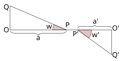
This aberration is quite distinct from that of the sharpness of reproduction; in unsharp, reproduction, the question of distortion arises if only parts of the object can be recognized in the figure. If, in an unsharp image, a patch of light corresponds to an object point, the center of gravity of the patch may be regarded as the image point, this being the point where the plane receiving the image, e.g., a focusing screen, intersects the ray passing through the middle of the stop. This assumption is justified if a poor image on the focusing screen remains stationary when the aperture is diminished; in practice, this generally occurs. This ray, named by Abbe a principal ray (not to be confused with the principal rays of the Gaussian theory), passes through the center of the entrance pupil before the first refraction, and the center of the exit pupil after the last refraction. From this it follows that correctness of drawing depends solely upon the principal rays; and is independent of the sharpness or curvature of the image field. Referring to fig. 4, we have O'Q'/OQ = a' tan w'/a tan w = 1/N, where N is the scale or magnification of the image. For N to be constant for all values of w, a' tan w'/a tan w must also be constant. If the ratio a'/a be sufficiently constant, as is often the case, the above relation reduces to the condition of Airy, i.e. tan w'/ tan w= a constant. This simple relation (see Camb. Phil. Trans., 1830, 3, p. 1) is fulfilled in all systems which are symmetrical with respect to their diaphragm (briefly named symmetrical or holosymmetrical objectives), or which consist of two like, but different-sized, components, placed from the diaphragm in the ratio of their size, and presenting the same curvature to it (hemisymmetrical objectives); in these systems tan w' / tan w = 1.
The constancy of a'/a necessary for this relation to hold was pointed out by R. H. Bow (Brit. Journ. Photog., 1861), and Thomas Sutton (Photographic Notes, 1862); it has been treated by O. Lummer and by M. von Rohr (Zeit. f. Instrumentenk., 1897, 17, and 1898, 18, p. 4). It requires the middle of the aperture stop to be reproduced in the centers of the entrance and exit pupils without spherical aberration. M. von Rohr showed that for systems fulfilling neither the Airy nor the Bow-Sutton condition, the ratio a' cos w'/a tan w will be constant for one distance of the object. This combined condition is exactly fulfilled by holosymmetrical objectives reproducing with the scale 1, and by hemisymmetrical, if the scale of reproduction be equal to the ratio of the sizes of the two components.
Zernike model of aberrations
Circular wavefront profiles associated with aberrations may be mathematically modeled using Zernike polynomials. Developed by Frits Zernike in the 1930s, Zernike's polynomials are orthogonal over a circle of unit radius. A complex, aberrated wavefront profile may be curve-fitted with Zernike polynomials to yield a set of fitting coefficients that individually represent different types of aberrations. These Zernike coefficients are linearly independent, thus individual aberration contributions to an overall wavefront may be isolated and quantified separately.There are even and odd Zernike polynomials. The even Zernike polynomials are defined as
The first few Zernike polynomials are:
| "Piston", equal to the mean value of the wavefront | |
| "X-Tilt", the deviation of the overall beam in the sagittal direction | |
| "Y-Tilt", the deviation of the overall beam in the tangential direction | |
| "Defocus", a parabolic wavefront resulting from being out of focus | |
| "0° Astigmatism", a cylindrical shape along the X or Y axis | |
| "45° Astigmatism", a cylindrical shape oriented at ±45° from the X axis | |
| "X-Coma", comatic image flaring in the horizontal direction | |
| "Y-Coma", comatic image flaring in the vertical direction | |
| "Third order spherical aberration" |
where is the normalized pupil radius with , is the azimuthal angle around the pupil with , and the fitting coefficients are the wavefront errors in wavelengths.
As in Fourier synthesis using sines and cosines, a wavefront may be perfectly represented by a sufficiently large number of higher-order Zernike polynomials. However, wavefronts with very steep gradients or very high spatial frequency structure, such as produced by propagation through atmospheric turbulence or aerodynamic flowfields, are not well modeled by Zernike polynomials, which tend to low-pass filter fine spatial definition in the wavefront. In this case, other fitting methods such as fractals or singular value decomposition may yield improved fitting results.
The circle polynomials were introduced by Frits Zernike to evaluate the point image of an aberrated optical system taking into account the effects of diffraction. The perfect point image in the presence of diffraction had already been described by Airy, as early as 1835. It took almost hundred years to arrive at a comprehensive theory and modeling of the point image of aberrated systems (Zernike and Nijboer). The analysis by Nijboer and Zernike describes the intensity distribution close to the optimum focal plane. An extended theory that allows the calculation of the point image amplitude and intensity over a much larger volume in the focal region was recently developed (Extended Nijboer-Zernike theory). This Extended Nijboer-Zernike theory of point image or ‘point-spread function’ formation has found applications in general research on image formation, especially for systems with a high numerical aperture, and in characterizing optical systems with respect to their aberrations.
Analytic treatment of aberrations
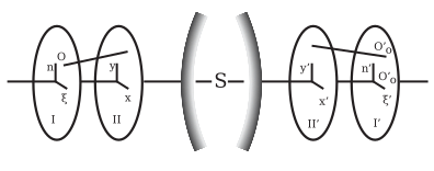
The preceding review of the several errors of reproduction belongs to the Abbe theory of aberrations, in which definite aberrations are discussed separately; it is well suited to practical needs, for in the construction of an optical instrument certain errors are sought to be eliminated, the selection of which is justified by experience. In the mathematical sense, however, this selection is arbitrary; the reproduction of a finite object with a finite aperture entails, in all probability, an infinite number of aberrations. This number is only finite if the object and aperture are assumed to be infinitely small of a certain order; and with each order of infinite smallness, i.e. with each degree of approximation to reality (to finite objects and apertures), a certain number of aberrations is associated. This connection is only supplied by theories which treat aberrations generally and analytically by means of indefinite series.A ray proceeding from an object point O (fig. 5) can be defined by the coordinates (ξ, η). Of this point O in an object plane I, at right angles to the axis, and two other coordinates (x, y), the point in which the ray intersects the entrance pupil, i.e. the plane II. Similarly the corresponding image ray may be defined by the points (ξ', η'), and (x', y'), in the planes I' and II'. The origins of these four plane coordinate systems may be collinear with the axis of the optical system; and the corresponding axes may be parallel. Each of the four coordinates ξ', η', x', y' are functions of ξ, η, x, y; and if it be assumed that the field of view and the aperture be infinitely small, then ξ, η, x, y are of the same order of infinitesimals; consequently by expanding ξ', η', x', y' in ascending powers of ξ, η, x, y, series are obtained in which it is only necessary to consider the lowest powers. It is readily seen that if the optical system be symmetrical, the origins of the coordinate systems collinear with the optical axis and the corresponding axes parallel, then by changing the signs of ξ, η, x, y, the values ξ', η', x', y' must likewise change their sign, but retain their arithmetical values; this means that the series are restricted to odd powers of the unmarked variables.
The nature of the reproduction consists in the rays proceeding from a point O being united in another point O'; in general, this will not be the case, for ξ', η' vary if ξ, η be constant, but x, y variable. It may be assumed that the planes I' and II' are drawn where the images of the planes I and II are formed by rays near the axis by the ordinary Gaussian rules; and by an extension of these rules, not, however, corresponding to reality, the Gauss image point O'0, with coordinates ξ'0, η'0, of the point O at some distance from the axis could be constructed. Writing Dξ'=ξ'-ξ'0 and Dη'=η'-η'0, then Dξ' and Dη' are the aberrations belonging to ξ, η and x, y, and are functions of these magnitudes which, when expanded in series, contain only odd powers, for the same reasons as given above. On account of the aberrations of all rays which pass through O, a patch of light, depending in size on the lowest powers of ξ, η, x, y which the aberrations contain, will be formed in the plane I'. These degrees, named by J. Petzval (Bericht uber die Ergebnisse einiger dioptrischer Untersuchungen, Buda Pesth, 1843; Akad. Sitzber., Wien, 1857, vols. xxiv. xxvi.) the numerical orders of the image, are consequently only odd powers; the condition for the formation of an image of the mth order is that in the series for Dξ' and Dη' the coefficients of the powers of the 3rd, 5th…(m-2)th degrees must vanish. The images of the Gauss theory being of the third order, the next problem is to obtain an image of 5th order, or to make the coefficients of the powers of 3rd degree zero. This necessitates the satisfying of five equations; in other words, there are five alterations of the 3rd order, the vanishing of which produces an image of the 5th order.
The expression for these coefficients in terms of the constants of the optical system, i.e. the radii, thicknesses, refractive indices and distances between the lenses, was solved by L. Seidel (Astr. Nach., 1856, p. 289); in 1840, J. Petzval constructed his portrait objective, from similar calculations which have never been published (see M. von Rohr, Theorie und Geschichte des photographischen Objectivs, Berlin, 1899, p. 248). The theory was elaborated by S. Finterswalder (Munchen. Acad. Abhandl., 1891, 17, p. 519), who also published a posthumous paper of Seidel containing a short view of his work (München. Akad. Sitzber., 1898, 28, p. 395); a simpler form was given by A. Kerber (Beiträge zur Dioptrik, Leipzig, 1895-6-7-8-9). A. Konig and M. von Rohr (see M. von Rohr, Die Bilderzeugung in optischen Instrumenten, pp. 317–323) have represented Kerber's method, and have deduced the Seidel formulae from geometrical considerations based on the Abbe method, and have interpreted the analytical results geometrically (pp. 212–316).
The aberrations can also be expressed by means of the characteristic function of the system and its differential coefficients, instead of by the radii, &c., of the lenses; these formulae are not immediately applicable, but give, however, the relation between the number of aberrations and the order. Sir William Rowan Hamilton (British Assoc. Report, 1833, p. 360) thus derived the aberrations of the third order; and in later times the method was pursued by Clerk Maxwell (Proc. London Math. Soc., 1874–1875; (see also the treatises of R. S. Heath and L. A. Herman), M. Thiesen (Berlin. Akad. Sitzber., 1890, 35, p. 804), H. Bruns (Leipzig. Math. Phys. Ber., 1895, 21, p. 410), and particularly successfully by K. Schwarzschild (Göttingen. Akad. Abhandl., 1905, 4, No. 1), who thus discovered the aberrations of the 5th order (of which there are nine), and possibly the shortest proof of the practical (Seidel) formulae. A. Gullstrand (vide supra, and Ann. d. Phys., 1905, 18, p. 941) founded his theory of aberrations on the differential geometry of surfaces.
The aberrations of the third order are: (1) aberration of the axis point; (2) aberration of points whose distance from the axis is very small, less than of the third order — the deviation from the sine condition and coma here fall together in one class; (3) astigmatism; (4) curvature of the field; (5) distortion.
- (1) Aberration of the third order of axis points is dealt with in all text-books on optics. It is very important in telescope design. In telescopes aperture is usually taken as the linear diameter of the objective. It is not the same as microscope aperture which is based on the entrance pupil or field of view as seen from the object and is expressed as an angular measurement. Higher order aberrations in telescope design can be mostly neglected. For microscopes it cannot be neglected. For a single lens of very small thickness and given power, the aberration depends upon the ratio of the radii r:r', and is a minimum (but never zero) for a certain value of this ratio; it varies inversely with the refractive index (the power of the lens remaining constant). The total aberration of two or more very thin lenses in contact, being the sum of the individual aberrations, can be zero. This is also possible if the lenses have the same algebraic sign. Of thin positive lenses with n=1.5, four are necessary to correct spherical aberration of the third order. These systems, however, are not of great practical importance. In most cases, two thin lenses are combined, one of which has just so strong a positive aberration (under-correction, vide supra) as the other a negative; the first must be a positive lens and the second a negative lens; the powers, however: may differ, so that the desired effect of the lens is maintained. It is generally an advantage to secure a great refractive effect by several weaker than by one high-power lens. By one, and likewise by several, and even by an infinite number of thin lenses in contact, no more than two axis points can be reproduced without aberration of the third order. Freedom from aberration for two axis points, one of which is infinitely distant, is known as Herschel's condition. All these rules are valid, inasmuch as the thicknesses and distances of the lenses are not to be taken into account.
- (2) The condition for freedom from coma in the third order is also of importance for telescope objectives; it is known as Fraunhofer's condition. (4) After eliminating the aberration On the axis, coma and astigmatism, the relation for the flatness of the field in the third order is expressed by the Petzval equation, S1/r(n'-n) = 0, where r is the radius of a refracting surface, n and n' the refractive indices of the neighboring media, and S the sign of summation for all refracting surfaces.
Practical elimination of aberrations
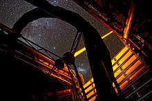
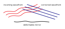
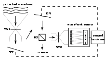
Laser guide stars assist in the elimination of atmospheric distortion.
The classical imaging problem is to reproduce perfectly a finite plane (the object) onto another plane (the image) through a finite aperture. It is impossible to do so perfectly for more than one such pair of planes (this was proven with increasing generality by Maxwell in 1858, by Bruns in 1895, and by Carathéodory in 1926, see summary in Walther, A., J. Opt. Soc. Am. A 6, 415–422 (1989)). For a single pair of planes (e.g. for a single focus setting of an objective), however, the problem can in principle be solved perfectly. Examples of such a theoretically perfect system include the Luneburg lens and the Maxwell fish-eye.
Practical methods solve this problem with an accuracy which mostly suffices for the special purpose of each species of instrument. The problem of finding a system which reproduces a given object upon a given plane with given magnification (insofar as aberrations must be taken into account) could be dealt with by means of the approximation theory; in most cases, however, the analytical difficulties were too great for older calculation methods but may be ameliorated by application of modern computer systems. Solutions, however, have been obtained in special cases (see A. Konig in M. von Rohr's Die Bilderzeugung, p. 373; K. Schwarzschild, Göttingen. Akad. Abhandl., 1905, 4, Nos. 2 and 3). At the present time constructors almost always employ the inverse method: they compose a system from certain, often quite personal experiences, and test, by the trigonometrical calculation of the paths of several rays, whether the system gives the desired reproduction (examples are given in A. Gleichen, Lehrbuch der geometrischen Optik, Leipzig and Berlin, 1902). The radii, thicknesses and distances are continually altered until the errors of the image become sufficiently small. By this method only certain errors of reproduction are investigated, especially individual members, or all, of those named above. The analytical approximation theory is often employed provisionally, since its accuracy does not generally suffice.
In order to render spherical aberration and the deviation from the sine condition small throughout the whole aperture, there is given to a ray with a finite angle of aperture u* (width infinitely distant objects: with a finite height of incidence h*) the same distance of intersection, and the same sine ratio as to one neighboring the axis (u* or h* may not be much smaller than the largest aperture U or H to be used in the system). The rays with an angle of aperture smaller than u* would not have the same distance of intersection and the same sine ratio; these deviations are called zones, and the constructor endeavors to reduce these to a minimum. The same holds for the errors depending upon the angle of the field of view, w: astigmatism, curvature of field and distortion are eliminated for a definite value, w*, zones of astigmatism, curvature of field and distortion, attend smaller values of w. The practical optician names such systems: corrected for the angle of aperture u* (the height of incidence h*) or the angle of field of view w*. Spherical aberration and changes of the sine ratios are often represented graphically as functions of the aperture, in the same way as the deviations of two astigmatic image surfaces of the image plane of the axis point are represented as functions of the angles of the field of view.
The final form of a practical system consequently rests on compromise; enlargement of the aperture results in a diminution of the available field of view, and vice versa. But the larger aperture will give the larger resolution. The following may be regarded as typical:
- (1) Largest aperture; necessary corrections are — for the axis point, and sine condition; errors of the field of view are almost disregarded; example — high-power microscope objectives.
- (2) Wide angle lens; necessary corrections are — for astigmatism, curvature of field and distortion; errors of the aperture only slightly regarded; examples — photographic widest angle objectives and oculars.
- Between these extreme examples stands the normal lens: this is corrected more with regard to aperture; objectives for groups more with regard to the field of view.
- (3) Long focus lenses have small fields of view and aberrations on axis are very important. Therefore zones will be kept as small as possible and design should emphasize simplicity. Because of this these lenses are the best for analytical computation.
Chromatic or color aberration
In optical systems composed of lenses, the position, magnitude and errors of the image depend upon the refractive indices of the glass employed (see Lens (optics) and Monochromatic aberration, above). Since the index of refraction varies with the color or wavelength of the light (see dispersion), it follows that a system of lenses (uncorrected) projects images of different colors in somewhat different places and sizes and with different aberrations; i.e. there are chromatic differences of the distances of intersection, of magnifications, and of monochromatic aberrations. If mixed light be employed (e.g. white light) all these images are formed and they cause a confusion, named chromatic aberration; for instance, instead of a white margin on a dark background, there is perceived a colored margin, or narrow spectrum. The absence of this error is termed achromatism, and an optical system so corrected is termed achromatic. A system is said to be chromatically under-corrected when it shows the same kind of chromatic error as a thin positive lens, otherwise it is said to be overcorrected.If, in the first place, monochromatic aberrations be neglected — in other words, the Gaussian theory be accepted — then every reproduction is determined by the positions of the focal planes, and the magnitude of the focal lengths, or if the focal lengths, as ordinarily happens, be equal, by three constants of reproduction. These constants are determined by the data of the system (radii, thicknesses, distances, indices, etc., of the lenses); therefore their dependence on the refractive index, and consequently on the color, are calculable. The refractive indices for different wavelengths must be known for each kind of glass made use of. In this manner the conditions are maintained that any one constant of reproduction is equal for two different colors, i.e. this constant is achromatized. For example, it is possible, with one thick lens in air, to achromatize the position of a focal plane of the magnitude of the focal length. If all three constants of reproduction be achromatized, then the Gaussian image for all distances of objects is the same for the two colors, and the system is said to be in stable achromatism.
In practice it is more advantageous (after Abbe) to determine the chromatic aberration (for instance, that of the distance of intersection) for a fixed position of the object, and express it by a sum in which each component conlins the amount due to each refracting surface. In a plane containing the image point of one color, another colour produces a disk of confusion; this is similar to the confusion caused by two zones in spherical aberration. For infinitely distant objects the radius Of the chromatic disk of confusion is proportional to the linear aperture, and independent of the focal length (vide supra, Monochromatic Aberration of the Axis Point); and since this disk becomes the less harmful with an increasing image of a given object, or with increasing focal length, it follows that the deterioration of the image is proportional to the ratio of the aperture to the focal length, i.e. the relative aperture. (This explains the gigantic focal lengths in vogue before the discovery of achromatism.)
Examples:
- (a) In a very thin lens, in air, only one constant of reproduction is to be observed, since the focal length and the distance of the focal point are equal. If the refractive index for one color be , and for another , and the powers, or reciprocals of the focal lengths, be and , then (1) ; is called the dispersion, and the dispersive power of the glass.
- (b) Two thin lenses in contact: let and be the powers corresponding to the lenses of refractive indices and and radii , , and , respectively; let denote the total power, and , , the changes of , , and with the color. Then the following relations hold:
-
- (2) ; and
-
- (3) . For achromatism , hence, from (3),
-
- (4) , or . Therefore and must have different algebraic signs, or the system must be composed of a collective and a dispersive lens. Consequently the powers of the two must be different (in order that be not zero (equation 2)), and the dispersive powers must also be different (according to 4).
Glass with weaker dispersive power (greater ) is named crown glass; that with greater dispersive power, flint glass. For the construction of an achromatic collective lens ( positive) it follows, by means of equation (4), that a collective lens I. of crown glass and a dispersive lens II. of flint glass must be chosen; the latter, although the weaker, corrects the other chromatically by its greater dispersive power. For an achromatic dispersive lens the converse must be adopted. This is, at the present day, the ordinary type, e.g., of telescope objective; the values of the four radii must satisfy the equations (2) and (4). Two other conditions may also be postulated: one is always the elimination of the aberration on the axis; the second either the Herschel or Fraunhofer Condition, the latter being the best vide supra, Monochromatic Aberration). In practice, however, it is often more useful to avoid the second condition by making the lenses have contact, i.e. equal radii. According to P. Rudolph (Eder's Jahrb. f. Photog., 1891, 5, p. 225; 1893, 7, p. 221), cemented objectives of thin lenses permit the elimination of spherical aberration on the axis, if, as above, the collective lens has a smaller refractive index; on the other hand, they permit the elimination of astigmatism and curvature of the field, if the collective lens has a greater refractive index (this follows from the Petzval equation; see L. Seidel, Astr. Nachr., 1856, p. 289). Should the cemented system be positive, then the more powerful lens must be positive; and, according to (4), to the greater power belongs the weaker dispersive power (greater ), that is to say, crown glass; consequently the crown glass must have the greater refractive index for astigmatic and plane images. In all earlier kinds of glass, however, the dispersive power increased with the refractive index; that is, decreased as increased; but some of the Jena glasses by E. Abbe and O. Schott were crown glasses of high refractive index, and achromatic systems from such crown glasses, with flint glasses of lower refractive index, are called the new achromats, and were employed by P. Rudolph in the first anastigmats (photographic objectives).
Instead of making vanish, a certain value can be assigned to it which will produce, by the addition of the two lenses, any desired chromatic deviation, e.g. sufficient to eliminate one present in other parts of the system. If the lenses I. and II. be cemented and have the same refractive index for one color, then its effect for that one color is that of a lens of one piece; by such decomposition of a lens it can be made chromatic or achromatic at will, without altering its spherical effect. If its chromatic effect () be greater than that of the same lens, this being made of the more dispersive of the two glasses employed, it is termed hyper-chromatic.
For two thin lenses separated by a distance the condition for achromatism is ; if (e.g. if the lenses be made of the same glass), this reduces to , known as the condition for oculars.
If a constant of reproduction, for instance the focal length, be made equal for two colors, then it is not the same for other colors, if two different glasses are employed. For example, the condition for achromatism (4) for two thin lenses in contact is fulfilled in only one part of the spectrum, since varies within the spectrum. This fact was first ascertained by J. Fraunhofer, who defined the colors by means of the dark lines in the solar spectrum; and showed that the ratio of the dispersion of two glasses varied about 20% from the red to the violet (the variation for glass and water is about 50%). If, therefore, for two colors, a and b, , then for a third color, c, the focal length is different; that is, if c lies between a and b, then , and vice versa; these algebraic results follow from the fact that towards the red the dispersion of the positive crown glass preponderates, towards the violet that of the negative flint. These chromatic errors of systems, which are achromatic for two colors, are called the secondary spectrum, and depend upon the aperture and focal length in the same manner as the primary chromatic errors do.
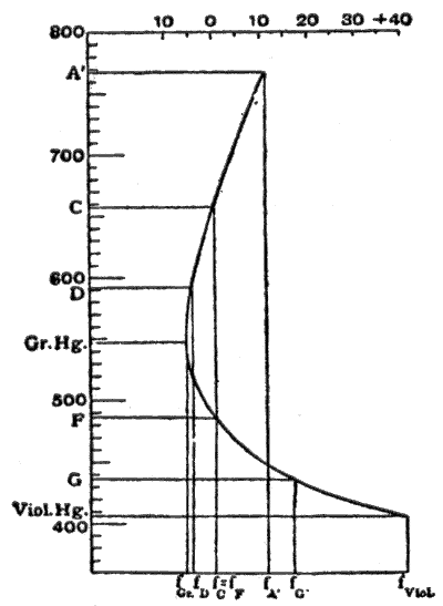
In fig. 6, taken from M. von Rohr's Theorie und Geschichte des photographischen Objectivs, the abscissae are focal lengths, and the ordinates wavelengths. The Fraunhofer lines used are shown in adjacent table.
| A' | C | D | Green Hg. | F | G' | Violet Hg. |
| 767.7 | 656.3 | 589.3 | 546.1 | 486.2 | 454.1 | 405.1 nm |
The focal lengths are made equal for the lines C and F. In the neighborhood of 550 nm the tangent to the curve is parallel to the axis of wavelengths; and the focal length varies least over a fairly large range of color, therefore in this neighborhood the color union is at its best. Moreover, this region of the spectrum is that which appears brightest to the human eye, and consequently this curve of the secondary on spectrum, obtained by making , is, according to the experiments of Sir G. G. Stokes (Proc. Roy. Soc., 1878), the most suitable for visual instruments (optical achromatism,). In a similar manner, for systems used in photography, the vertex of the color curve must be placed in the position of the maximum sensibility of the plates; this is generally supposed to be at G'; and to accomplish this the F and violet mercury lines are united. This artifice is specially adopted in objectives for astronomical photography (pure actinic achromatism). For ordinary photography, however, there is this disadvantage: the image on the focusing-screen and the correct adjustment of the photographic sensitive plate are not in register; in astronomical photography this difference is constant, but in other kinds it depends on the distance of the objects. On this account the lines D and G' are united for ordinary photographic objectives; the optical as well as the actinic image is chromatically inferior, but both lie in the same place; and consequently the best correction lies in F (this is known as the actinic correction or freedom from chemical focus).
Should there be in two lenses in contact the same focal lengths for three colours a, b, and c, i.e. , then the relative partial dispersion must be equal for the two kinds of glass employed. This follows by considering equation (4) for the two pairs of colors ac and bc. Until recently no glasses were known with a proportional degree of absorption; but R. Blair (Trans. Edin. Soc., 1791, 3, p. 3), P. Barlow, and F. S. Archer overcame the difficulty by constructing fluid lenses between glass walls. Fraunhofer prepared glasses which reduced the secondary spectrum; but permanent success was only assured on the introduction of the Jena glasses by E. Abbe and O. Schott. In using glasses not having proportional dispersion, the deviation of a third colour can be eliminated by two lenses, if an interval be allowed between them; or by three lenses in contact, which may not all consist of the old glasses. In uniting three colors an achromatism of a higher order is derived; there is yet a residual tertiary spectrum, but it can always be neglected.
The Gaussian theory is only an approximation; monochromatic or spherical aberrations still occur, which will be different for different colors; and should they be compensated for one color, the image of another color would prove disturbing. The most important is the chromatic difference of aberration of the axis point, which is still present to disturb the image, after par-axial rays of different colors are united by an appropriate combination of glasses. If a collective system be corrected for the axis point for a definite wavelength, then, on account of the greater dispersion in the negative components — the flint glasses, — overcorrection will arise for the shorter wavelengths (this being the error of the negative components), and under-correction for the longer wavelengths (the error of crown glass lenses preponderating in the red). This error was treated by Jean le Rond d'Alembert, and, in special detail, by C. F. Gauss. It increases rapidly with the aperture, and is more important with medium apertures than the secondary spectrum of par-axial rays; consequently, spherical aberration must be eliminated for two colors, and if this be impossible, then it must be eliminated for those particular wavelengths which are most effectual for the instrument in question (a graphical representation of this error is given in M. von Rohr, Theorie und Geschichte des photographischen Objectivs).
The condition for the reproduction of a surface element in the place of a sharply reproduced point — the constant of the sine relationship must also be fulfilled with large apertures for several colors. E. Abbe succeeded in computing microscope objectives free from error of the axis point and satisfying the sine condition for several colors, which therefore, according to his definition, were aplanatic for several colors; such systems he termed apochromatic. While, however, the magnification of the individual zones is the same, it is not the same for red as for blue; and there is a chromatic difference of magnification. This is produced in the same amount, but in the opposite sense, by the oculars, which Abbe used with these objectives (compensating oculars), so that it is eliminated in the image of the whole microscope. The best telescope objectives, and photographic objectives intended for three-color work, are also apochromatic, even if they do not possess quite the same quality of correction as microscope objectives do. The chromatic differences of other errors of reproduction have seldom practical importances.
