Digital electronics is a field of electronics involving the study of digital signals and the engineering of devices that use or produce them. This is in contrast to analog electronics which work primarily with analog signals. Despite the name, digital electronics designs includes important analog design considerations.
Digital electronic circuits are usually made from large assemblies of logic gates, often packaged in integrated circuits. Complex devices may have simple electronic representations of Boolean logic functions.
History
The binary number system was refined by Gottfried Wilhelm Leibniz (published in 1705) and he also established that by using the binary system, the principles of arithmetic and logic could be joined. Digital logic as we know it was the brain-child of George Boole in the mid 19th century. In an 1886 letter, Charles Sanders Peirce described how logical operations could be carried out by electrical switching circuits. Eventually, vacuum tubes replaced relays for logic operations. Lee De Forest's modification of the Fleming valve in 1907 could be used as an AND gate. Ludwig Wittgenstein introduced a version of the 16-row truth table as proposition 5.101 of Tractatus Logico-Philosophicus (1921). Walther Bothe, inventor of the coincidence circuit, shared the 1954 Nobel Prize in physics, for creating the first modern electronic AND gate in 1924.
Mechanical analog computers started appearing in the first century and were later used in the medieval era for astronomical calculations. In World War II, mechanical analog computers were used for specialized military applications such as calculating torpedo aiming. During this time the first electronic digital computers were developed, with the term digital being proposed by George Stibitz in 1942. Originally they were the size of a large room, consuming as much power as several hundred modern PCs.
The Z3 was an electromechanical computer designed by Konrad Zuse. Finished in 1941, it was the world's first working programmable, fully automatic digital computer. Its operation was facilitated by the invention of the vacuum tube in 1904 by John Ambrose Fleming.
At the same time that digital calculation replaced analog, purely electronic circuit elements soon replaced their mechanical and electromechanical equivalents. John Bardeen and Walter Brattain invented the point-contact transistor at Bell Labs in 1947, followed by William Shockley inventing the bipolar junction transistor at Bell Labs in 1948.
At the University of Manchester, a team under the leadership of Tom Kilburn designed and built a machine using the newly developed transistors instead of vacuum tubes. Their "transistorised computer", and the first in the world, was operational by 1953, and a second version was completed there in April 1955. From 1955 and onwards, transistors replaced vacuum tubes in computer designs, giving rise to the "second generation" of computers. Compared to vacuum tubes, transistors were smaller, more reliable, had indefinite lifespans, and required less power than vacuum tubes - thereby giving off less heat, and allowing much denser concentrations of circuits, up to tens of thousands in a relatively compact space.
While working at Texas Instruments in July 1958, Jack Kilby recorded his initial ideas concerning the integrated circuit (IC), then successfully demonstrated the first working integrated circuit on 12 September 1958. Kilby's chip was made of germanium. The following year, Robert Noyce at Fairchild Semiconductor invented the silicon integrated circuit. The basis for Noyce's silicon IC was the planar process, developed in early 1959 by Jean Hoerni, who was in turn building on Mohamed Atalla's silicon surface passivation method developed in 1957. This new technique, the integrated circuit, allowed for quick, low-cost fabrication of complex circuits by having a set of electronic circuits on one small plate ("chip") of semiconductor material, normally silicon.
The metal–oxide–semiconductor field-effect transistor (MOSFET), also known as the MOS transistor, was invented by Mohamed Atalla and Dawon Kahng at Bell Labs in 1959. The MOSFET's advantages include high scalability, affordability, low power consumption, and high transistor density. Its rapid on–off electronic switching speed also makes it ideal for generating pulse trains, the basis for electronic digital signals, in contrast to BJTs which, more slowly, generate analog signals resembling sine waves. Along with MOS large-scale integration (LSI), these factors make the MOSFET an important switching device for digital circuits. The MOSFET revolutionized the electronics industry, and is the most common semiconductor device.
In the early days of integrated circuits, each chip was limited to only a few transistors, and the low degree of integration meant the design process was relatively simple. Manufacturing yields were also quite low by today's standards. The wide adoption of the MOSFET transistor by the early 1970s led to the first large-scale integration (LSI) chips with more than 10,000 transistors on a single chip. Following the wide adoption of CMOS, a type of MOSFET logic, by the 1980s, millions and then billions of MOSFETs could be placed on one chip as the technology progressed, and good designs required thorough planning, giving rise to new design methods. The transistor count of devices and total production rose to unprecedented heights. The total amount of transistors produced until 2018 has been estimated to be 1.3×10²² (13 sextillion).
The wireless revolution (the introduction and proliferation of wireless networks) began in the 1990s and was enabled by the wide adoption of MOSFET-based RF power amplifiers (power MOSFET and LDMOS) and RF circuits (RF CMOS). Wireless networks allowed for public digital transmission without the need for cables, leading to digital television, satellite and digital radio, GPS, wireless Internet and mobile phones through the 1990s–2000s.
Properties
An advantage of digital circuits when compared to analog circuits is that signals represented digitally can be transmitted without degradation caused by noise. For example, a continuous audio signal transmitted as a sequence of 1s and 0s, can be reconstructed without error, provided the noise picked up in transmission is not enough to prevent identification of the 1s and 0s.
In a digital system, a more precise representation of a signal can be obtained by using more binary digits to represent it. While this requires more digital circuits to process the signals, each digit is handled by the same kind of hardware, resulting in an easily scalable system. In an analog system, additional resolution requires fundamental improvements in the linearity and noise characteristics of each step of the signal chain.
With computer-controlled digital systems, new functions can be added through software revision and no hardware changes are needed. Often this can be done outside of the factory by updating the product's software. This way, the product's design errors can be corrected even after the product is in a customer's hands.
Information storage can be easier in digital systems than in analog ones. The noise immunity of digital systems permits data to be stored and retrieved without degradation. In an analog system, noise from aging and wear degrade the information stored. In a digital system, as long as the total noise is below a certain level, the information can be recovered perfectly. Even when more significant noise is present, the use of redundancy permits the recovery of the original data provided too many errors do not occur.
In some cases, digital circuits use more energy than analog circuits to accomplish the same tasks, thus producing more heat which increases the complexity of the circuits such as the inclusion of heat sinks. In portable or battery-powered systems this can limit the use of digital systems. For example, battery-powered cellular phones often use a low-power analog front-end to amplify and tune the radio signals from the base station. However, a base station has grid power and can use power-hungry, but very flexible software radios. Such base stations can easily be reprogrammed to process the signals used in new cellular standards.
Many useful digital systems must translate from continuous analog signals to discrete digital signals. This causes quantization errors. Quantization error can be reduced if the system stores enough digital data to represent the signal to the desired degree of fidelity. The Nyquist–Shannon sampling theorem provides an important guideline as to how much digital data is needed to accurately portray a given analog signal.
If a single piece of digital data is lost or misinterpreted, in some systems only a small error may result, while in other systems the meaning of large blocks of related data can completely change. For example, a single-bit error in audio data stored directly as linear pulse-code modulation causes, at worst, a single audible click. But when using audio compression to save storage space and transmission time, a single bit error may cause a much larger disruption.
Because of the cliff effect, it can be difficult for users to tell if a particular system is right on the edge of failure, or if it can tolerate much more noise before failing. Digital fragility can be reduced by designing a digital system for robustness. For example, a parity bit or other error management method can be inserted into the signal path. These schemes help the system detect errors, and then either correct the errors, or request retransmission of the data.
Construction

A digital circuit is typically constructed from small electronic circuits called logic gates that can be used to create combinational logic. Each logic gate is designed to perform a function of Boolean logic when acting on logic signals. A logic gate is generally created from one or more electrically controlled switches, usually transistors but thermionic valves have seen historic use. The output of a logic gate can, in turn, control or feed into more logic gates.
Another form of digital circuit is constructed from lookup tables, (many sold as "programmable logic devices", though other kinds of PLDs exist). Lookup tables can perform the same functions as machines based on logic gates, but can be easily reprogrammed without changing the wiring. This means that a designer can often repair design errors without changing the arrangement of wires. Therefore, in small volume products, programmable logic devices are often the preferred solution. They are usually designed by engineers using electronic design automation software.
Integrated circuits consist of multiple transistors on one silicon chip, and are the least expensive way to make large number of interconnected logic gates. Integrated circuits are usually interconnected on a printed circuit board which is a board which holds electrical components, and connects them together with copper traces.
Design
Engineers use many methods to minimize logic redundancy in order to reduce the circuit complexity. Reduced complexity reduces component count and potential errors and therefore typically reduces cost. Logic redundancy can be removed by several well-known techniques, such as binary decision diagrams, Boolean algebra, Karnaugh maps, the Quine–McCluskey algorithm, and the heuristic computer method. These operations are typically performed within a computer-aided design system.
Embedded systems with microcontrollers and programmable logic controllers are often used to implement digital logic for complex systems that do not require optimal performance. These systems are usually programmed by software engineers or by electricians, using ladder logic.
Representation
A digital circuit's input-output relationship can be represented as a truth table. An equivalent high-level circuit uses logic gates, each represented by a different shape (standardized by IEEE/ANSI 91–1984). A low-level representation uses an equivalent circuit of electronic switches (usually transistors).
Most digital systems divide into combinational and sequential systems. The output of a combinational system depends only on the present inputs. However, a sequential system has some of its outputs fed back as inputs, so its output may depend on past inputs in addition to present inputs, to produce a sequence of operations. Simplified representations of their behavior called state machines facilitate design and test.
Sequential systems divide into two further subcategories. "Synchronous" sequential systems change state all at once when a clock signal changes state. "Asynchronous" sequential systems propagate changes whenever inputs change. Synchronous sequential systems are made using flip flops that store inputted voltages as a bit only when the clock changes.
Synchronous systems

The usual way to implement a synchronous sequential state machine is to divide it into a piece of combinational logic and a set of flip flops called a state register. The state register represents the state as a binary number. The combinational logic produces the binary representation for the next state. On each clock cycle, the state register captures the feedback generated from the previous state of the combinational logic and feeds it back as an unchanging input to the combinational part of the state machine. The clock rate is limited by the most time-consuming logic calculation in the combinational logic.
Asynchronous systems
Most digital logic is synchronous because it is easier to create and verify a synchronous design. However, asynchronous logic has the advantage of its speed not being constrained by an arbitrary clock; instead, it runs at the maximum speed of its logic gates. Nevertheless, most systems need to accept external unsynchronized signals into their synchronous logic circuits. This interface is inherently asynchronous and must be analyzed as such. Examples of widely used asynchronous circuits include synchronizer flip-flops, switch debouncers and arbiters.
Asynchronous logic components can be hard to design because all possible states, in all possible timings must be considered. The usual method is to construct a table of the minimum and maximum time that each such state can exist and then adjust the circuit to minimize the number of such states. The designer must force the circuit to periodically wait for all of its parts to enter a compatible state (this is called "self-resynchronization"). Without careful design, it is easy to accidentally produce asynchronous logic that is unstable—that is—real electronics will have unpredictable results because of the cumulative delays caused by small variations in the values of the electronic components.
Register transfer systems

Many digital systems are data flow machines. These are usually designed using synchronous register transfer logic and written with hardware description languages such as VHDL or Verilog.
In register transfer logic, binary numbers are stored in groups of flip flops called registers. A sequential state machine controls when each register accepts new data from its input. The outputs of each register are a bundle of wires called a bus that carries that number to other calculations. A calculation is simply a piece of combinational logic. Each calculation also has an output bus, and these may be connected to the inputs of several registers. Sometimes a register will have a multiplexer on its input so that it can store a number from any one of several buses.
Asynchronous register-transfer systems (such as computers) have a general solution. In the 1980s, some researchers discovered that almost all synchronous register-transfer machines could be converted to asynchronous designs by using first-in-first-out synchronization logic. In this scheme, the digital machine is characterized as a set of data flows. In each step of the flow, a synchronization circuit determines when the outputs of that step are valid and instructs the next stage when to use these outputs.
Computer design
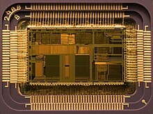
The most general-purpose register-transfer logic machine is a computer. This is basically an automatic binary abacus. The control unit of a computer is usually designed as a microprogram run by a microsequencer. A microprogram is much like a player-piano roll. Each table entry of the microprogram commands the state of every bit that controls the computer. The sequencer then counts, and the count addresses the memory or combinational logic machine that contains the microprogram. The bits from the microprogram control the arithmetic logic unit, memory and other parts of the computer, including the microsequencer itself. In this way, the complex task of designing the controls of a computer is reduced to the simpler task of programming a collection of much simpler logic machines.
Almost all computers are synchronous. However, asynchronous computers have also been built. One example is the ASPIDA DLX core. Another was offered by ARM Holdings. They do not, however, have any speed advantages because modern computer designs already run at the speed of their slowest component, usually memory. They do use somewhat less power because a clock distribution network is not needed. An unexpected advantage is that asynchronous computers do not produce spectrally-pure radio noise. They are used in some radio-sensitive mobile-phone base-station controllers. They may be more secure in cryptographic applications because their electrical and radio emissions can be more difficult to decode.
Computer architecture
Computer architecture is a specialized engineering activity that tries to arrange the registers, calculation logic, buses and other parts of the computer in the best way possible for a specific purpose. Computer architects have put a lot of work into reducing the cost and increasing the speed of computers in addition to boosting their immunity to programming errors. An increasingly common goal of computer architects is to reduce the power used in battery-powered computer systems, such as smartphones.
Design issues in digital circuits
Digital circuits are made from analog components. The design must assure that the analog nature of the components does not dominate the desired digital behavior. Digital systems must manage noise and timing margins, parasitic inductances and capacitances.
Bad designs have intermittent problems such as glitches, vanishingly fast pulses that may trigger some logic but not others, runt pulses that do not reach valid threshold voltages.
Additionally, where clocked digital systems interface to analog systems or systems that are driven from a different clock, the digital system can be subject to metastability where a change to the input violates the setup time for a digital input latch.
Since digital circuits are made from analog components, digital circuits calculate more slowly than low-precision analog circuits that use a similar amount of space and power. However, the digital circuit will calculate more repeatably, because of its high noise immunity.
Automated design tools
Much of the effort of designing large logic machines has been automated through the application of electronic design automation (EDA).
Simple truth table-style descriptions of logic are often optimized with EDA that automatically produce reduced systems of logic gates or smaller lookup tables that still produce the desired outputs. The most common example of this kind of software is the Espresso heuristic logic minimizer. Optimizing large logic systems may be done using the Quine–McCluskey algorithm or binary decision diagrams. There are promising experiments with genetic algorithms and annealing optimizations.
To automate costly engineering processes, some EDA can take state tables that describe state machines and automatically produce a truth table or a function table for the combinational logic of a state machine. The state table is a piece of text that lists each state, together with the conditions controlling the transitions between them and their associated output signals.
Often, real logic systems are designed as a series of sub-projects, which are combined using a tool flow. The tool flow is usually controlled with the help of a scripting language, a simplified computer language that can invoke the software design tools in the right order. Tool flows for large logic systems such as microprocessors can be thousands of commands long, and combine the work of hundreds of engineers. Writing and debugging tool flows is an established engineering specialty in companies that produce digital designs. The tool flow usually terminates in a detailed computer file or set of files that describe how to physically construct the logic. Often it consists of instructions on how to draw the transistors and wires on an integrated circuit or a printed circuit board.
Parts of tool flows are debugged by verifying the outputs of simulated logic against expected inputs. The test tools take computer files with sets of inputs and outputs and highlight discrepancies between the simulated behavior and the expected behavior. Once the input data is believed to be correct, the design itself must still be verified for correctness. Some tool flows verify designs by first producing a design, then scanning the design to produce compatible input data for the tool flow. If the scanned data matches the input data, then the tool flow has probably not introduced errors.
The functional verification data are usually called test vectors. The functional test vectors may be preserved and used in the factory to test whether newly constructed logic works correctly. However, functional test patterns do not discover all fabrication faults. Production tests are often designed by automatic test pattern generation software tools. These generate test vectors by examining the structure of the logic and systematically generating tests targeting particular potential faults. This way the fault coverage can closely approach 100%, provided the design is properly made testable (see next section).
Once a design exists, and is verified and testable, it often needs to be processed to be manufacturable as well. Modern integrated circuits have features smaller than the wavelength of the light used to expose the photoresist. Software that are designed for manufacturability add interference patterns to the exposure masks to eliminate open-circuits, and enhance the masks' contrast.
Design for testability
There are several reasons for testing a logic circuit. When the circuit is first developed, it is necessary to verify that the design circuit meets the required functional, and timing specifications. When multiple copies of a correctly designed circuit are being manufactured, it is essential to test each copy to ensure that the manufacturing process has not introduced any flaws.
A large logic machine (say, with more than a hundred logical variables) can have an astronomical number of possible states. Obviously, factory testing every state of such a machine is unfeasible, for even if testing each state only took a microsecond, there are more possible states than there are microseconds since the universe began!
Large logic machines are almost always designed as assemblies of smaller logic machines. To save time, the smaller sub-machines are isolated by permanently installed design for test circuitry, and are tested independently. One common testing scheme provides a test mode that forces some part of the logic machine to enter a test cycle. The test cycle usually exercises large independent parts of the machine.
Boundary scan is a common test scheme that uses serial communication with external test equipment through one or more shift registers known as scan chains. Serial scans have only one or two wires to carry the data, and minimize the physical size and expense of the infrequently used test logic. After all the test data bits are in place, the design is reconfigured to be in normal mode and one or more clock pulses are applied, to test for faults (e.g. stuck-at low or stuck-at high) and capture the test result into flip-flops or latches in the scan shift register(s). Finally, the result of the test is shifted out to the block boundary and compared against the predicted good machine result.
In a board-test environment, serial to parallel testing has been formalized as the JTAG standard.
Trade-offs
Cost
Since a digital system may use many logic gates, the overall cost of building a computer correlates strongly with the cost of a logic gate. In the 1930s, the earliest digital logic systems were constructed from telephone relays because these were inexpensive and relatively reliable.
The earliest integrated circuits were constructed to save weight and permit the Apollo Guidance Computer to control an inertial guidance system for a spacecraft. The first integrated circuit logic gates cost nearly US$50, which in 2023 would be equivalent to $515. Mass-produced gates on integrated circuits became the least-expensive method to construct digital logic.
With the rise of integrated circuits, reducing the absolute number of chips used represented another way to save costs. The goal of a designer is not just to make the simplest circuit, but to keep the component count down. Sometimes this results in more complicated designs with respect to the underlying digital logic but nevertheless reduces the number of components, board size, and even power consumption.
Reliability
Another major motive for reducing component count on printed circuit boards is to reduce the manufacturing defect rate due to failed soldered connections and increase reliability. Defect and failure rates tend to increase along with the total number of component pins.
The failure of a single logic gate may cause a digital machine to fail. Where additional reliability is required, redundant logic can be provided. Redundancy adds cost and power consumption over a non-redundant system.
The reliability of a logic gate can be described by its mean time between failure (MTBF). Digital machines first became useful when the MTBF for a switch increased above a few hundred hours. Even so, many of these machines had complex, well-rehearsed repair procedures, and would be nonfunctional for hours because a tube burned-out, or a moth got stuck in a relay. Modern transistorized integrated circuit logic gates have MTBFs greater than 82 billion hours (8.2×10¹⁰ h). This level of reliability is required because integrated circuits have so many logic gates.
Fan-out
Fan-out describes how many logic inputs can be controlled by a single logic output without exceeding the electrical current ratings of the gate outputs. The minimum practical fan-out is about five. Modern electronic logic gates using CMOS transistors for switches have higher fan-outs.
Speed
The switching speed describes how long it takes a logic output to change from true to false or vice versa. Faster logic can accomplish more operations in less time. Modern electronic digital logic routinely switches at 5 GHz, and some laboratory systems switch at more than 1 THz.
Logic families
Digital design started with relay logic which is slow. Occasionally a mechanical failure would occur. Fan-outs were typically about 10, limited by the resistance of the coils and arcing on the contacts from high voltages.
Later, vacuum tubes were used. These were very fast, but generated heat, and were unreliable because the filaments would burn out. Fan-outs were typically 5 to 7, limited by the heating from the tubes' current. In the 1950s, special computer tubes were developed with filaments that omitted volatile elements like silicon. These ran for hundreds of thousands of hours.
The first semiconductor logic family was resistor–transistor logic. This was a thousand times more reliable than tubes, ran cooler, and used less power, but had a very low fan-out of 3. Diode–transistor logic improved the fan-out up to about 7, and reduced the power. Some DTL designs used two power-supplies with alternating layers of NPN and PNP transistors to increase the fan-out.
Transistor–transistor logic (TTL) was a great improvement over these. In early devices, fan-out improved to 10, and later variations reliably achieved 20. TTL was also fast, with some variations achieving switching times as low as 20 ns. TTL is still used in some designs.
Emitter coupled logic is very fast but uses a lot of power. It was extensively used for high-performance computers, such as the Illiac IV, made up of many medium-scale components.
By far, the most common digital integrated circuits built today use CMOS logic, which is fast, offers high circuit density and low power per gate. This is used even in large, fast computers, such as the IBM System z.
Recent developments
In 2009, researchers discovered that memristors can implement a Boolean state storage and provides a complete logic family with very small amounts of space and power, using familiar CMOS semiconductor processes.
The discovery of superconductivity has enabled the development of rapid single flux quantum (RSFQ) circuit technology, which uses Josephson junctions instead of transistors. Most recently, attempts are being made to construct purely optical computing systems capable of processing digital information using nonlinear optical elements.


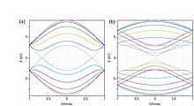


![{\displaystyle \theta =\tan ^{-1}[{\sqrt {3}}\,n/(2m+n)]}](https://wikimedia.org/api/rest_v1/media/math/render/svg/44bdad0652d145e2caa1f557844d5425bde736a5)


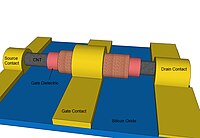
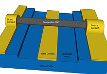


![{\displaystyle I_{DS}={\frac {2qkT}{\pi {\hbar }}}\left[F_{0}\left({\frac {U_{SF}}{kT}}\right)-F_{0}\left({\frac {U_{DF}}{kT}}\right)\right]}](https://wikimedia.org/api/rest_v1/media/math/render/svg/bad7659b78100973438a38557bb8d1c827f1df32)