A passive infrared sensor (PIR sensor) is an electronic sensor that measures infrared (IR) light radiating from objects in its field of view. They are most often used in PIR-based motion detectors.
PIR sensors are commonly used in security alarms and automatic lighting
applications. PIR sensors detect general movement, but do not give
information on who or what moved. For that purpose, an active IR sensor is required.
PIR sensors are commonly called simply "PIR", or sometimes "PID", for "passive infrared detector". The term passive refers to the fact that PIR devices do not radiate energy for detection purposes. They work entirely by detecting infrared radiation (radiant heat) emitted by or reflected from objects.
Operating principles
All objects with a temperature above absolute zero emit heat energy in the form of radiation. Usually this radiation isn't visible to the human eye because it radiates at infrared wavelengths, but it can be detected by electronic devices designed for such a purpose.
Construction
Infrared radiation enters through the front of the sensor, known as the 'sensor face'. At the core of a PIR sensor is a solid state sensor or set of sensors, made from pyroelectric materials—materials which generate energy when exposed to heat. Typically, the sensors are approximately 1/4 inch square (40 mm2), and take the form of a thin film. Materials commonly used in PIR sensors include gallium nitride (GaN), caesium nitrate (CsNO3), polyvinyl fluorides, derivatives of phenylpyridine, and cobaltphthalocyanine. The sensor is often manufactured as part of an integrated circuit.
PIR-based motion detector
A PIR motion detector used to control an outdoor, automatic light.
A PIR-based motion detector is used to sense movement of people, animals, or other objects. They are commonly used in burglar alarms and automatically-activated lighting systems.
Operation
A
PIR sensor can detect changes in the amount of infrared radiation
impinging upon it, which varies depending on the temperature and surface
characteristics of the objects in front of the sensor.
When an object, such as a person, passes in front of the background,
such as a wall, the temperature at that point in the sensor's field of
view will rise from room temperature to body temperature,
and then back again. The sensor converts the resulting change in the
incoming infrared radiation into a change in the output voltage, and
this triggers the detection. Objects of similar temperature but
different surface characteristics may also have a different infrared
emission pattern, and thus moving them with respect to the background
may trigger the detector as well.
PIRs come in many configurations for a wide variety of applications. The most common models have numerous Fresnel lenses
or mirror segments, an effective range of about 10 meters (30 feet),
and a field of view less than 180°. Models with wider fields of view,
including 360°, are available, typically designed to mount on a ceiling.
Some larger PIRs are made with single segment mirrors and can sense
changes in infrared energy over 30 meters (100 feet) from the PIR. There
are also PIRs designed with reversible orientation mirrors which allow
either broad coverage (110° wide) or very narrow "curtain" coverage, or
with individually selectable segments to "shape" the coverage.
Differential detection
Pairs of sensor elements may be wired as opposite inputs to a differential amplifier.
In such a configuration, the PIR measurements cancel each other so that
the average temperature of the field of view is removed from the
electrical signal; an increase of IR energy across the entire sensor is
self-cancelling and will not trigger the device. This allows the device
to resist false indications of change in the event of being exposed to
brief flashes of light or field-wide illumination. (Continuous high
energy exposure may still be able to saturate the sensor materials and
render the sensor unable to register further information.) At the same
time, this differential arrangement minimizes common-mode interference,
allowing the device to resist triggering due to nearby electric fields.
However, a differential pair of sensors cannot measure temperature in
this configuration, and therefore is only useful for motion detection.
Practical Implementation
When
a PIR sensor is configured in a differential mode, it specifically
becomes applicable as a motion detector device. In this mode when a
movement is detected within the "line of sight" of the sensor, a pair of
complementary pulses
are processed at the output pin of the sensor. In order to implement
this output signal for a practical triggering of a load such as a relay
or a data logger, or an alarm,
the differential signal is rectified using a bridge rectifier and fed
to a transistorized relay driver circuit. The contacts of this relay
close and open in response to the signals from the PIR, activating the
attached load across its contacts, acknowledging the detection of a
person within the predetermined restricted area.
Product design
The PIR sensor is typically mounted on a printed circuit board
containing the necessary electronics required to interpret the signals
from the sensor itself. The complete assembly is usually contained
within a housing, mounted in a location where the sensor can cover the
area to be monitored.
PIR motion sensor design
The housing will usually have a plastic "window" through which the infrared energy can enter. Despite often being only translucent to visible light, infrared energy is able to reach the sensor through the window because the plastic used is transparent
to infrared radiation. The plastic window reduces the chance of foreign
objects (dust, insects, etc.) from obscuring the sensor's field of
view, damaging the mechanism, and/or causing false alarms.
The window may be used as a filter, to limit the wavelengths to 8-14
micrometres, which is closest to the infrared radiation emitted by
humans. It may also serve as a focusing mechanism; see below.
Focusing
Different mechanisms can be used to focus the distant infrared energy onto the sensor surface.
Lenses
The plastic window covering may have multiple facets molded into it, to focus the infrared energy onto the sensor. Each individual facet is a Fresnel lens.
Multi-Fresnel lens type of PIR
PIR motion detector housing with cylindrical faceted window. The
animation highlights individual facets, each of which is a Fresnel lens,
focusing light on the sensor element underneath.
PIR front cover only (electronics removed), with point light source behind, to show individual lenses.
PIR with front cover removed, showing location of pyroelectric sensor (green arrow).
Mirrors
Some PIRs are manufactured with internal, segmented parabolic mirrors to focus the infrared energy. Where mirrors are used, the plastic window cover generally has no Fresnel lenses molded into it.
Segmented mirror type of PIR
Typical residential/commercial PID using an internal segmented mirror for focusing.
Cover removed. Segmented mirror at bottom with PC (printed circuit) board above it.
Printed circuit board removed to show segmented mirror.
Segmented parabolic mirror removed from housing.
Rear of circuit board which faces mirror when in place. Pyroelectric sensor indicated by green arrow.
Beam pattern
As
a result of the focussing, the detector view is actually a beam
pattern. Under certain angles (zones), the PIR sensor receives almost no
radiation energy and under other angles the PIR receives concentrated
amounts of infrared energy. This separation helps the motion detector to
discriminate between field-wide illumination and moving objects.
When a person walks from one angle (beam) to another, the
detector will only intermittently see the moving person. This results in
a rapidly changing sensor signal which is used by the electronics to
trigger an alarm or to turn on lighting. A slowly changing signal will
be ignored by the electronics.
The number, shape, distribution and sensitivity of these zones
are determined by the lens and/or mirror. Manufacturers do their best to
create the optimal sensitivity beam pattern for each application.
Motion detector with superimposed beam pattern. The length of the
beams is a measure of the detectors sensitivity in that direction.
Automatic lighting applications
When
used as part of a lighting system, the electronics in the PIR typically
control an integral relay capable of switching mains voltage. This
means the PIR can be set up to turn on lights that are connected to the
PIR when movement is detected. This is most commonly used in outdoor
scenarios either to deter criminals (security lighting) or for practical
uses like the front door light turning on so you can find your keys in
the dark.
Additional uses can be in public toilets, walk-in pantries, hallways or
anywhere that automatic control of lights is useful. This can provide
energy savings as the lights are only turned on when they are needed and
there is no reliance on users remembering to turn the lights off when
they leave the area.
Security applications
When used as part of a security system, the electronics in the PIR typically control a small relay. This relay completes the circuit across a pair of electrical contacts connected to a detection input zone of the burglar alarm control panel.
The system is usually designed such that if no motion is being
detected, the relay contact is closed—a 'normally closed' (NC) relay. If
motion is detected, the relay will open the circuit, triggering the
alarm; or, if a wire is disconnected, the alarm will also operate.
Placement
Manufacturers
recommend careful placement of their products to prevent false alarms
(i.e., any detection not caused by an intruder).
They suggest mounting the PIRs in such a way that the PIR cannot "see" out of a window. Although the wavelength
of infrared radiation to which the chips are sensitive does not
penetrate glass very well, a strong infrared source (such as from a
vehicle headlight or sunlight) can overload the sensor and cause a false
alarm. A person moving on the other side of the glass would not be
"seen" by the PID. That may be good for a window facing a public
sidewalk, or bad for a window in an interior partition.
It is also recommended that the PIR not be placed in such a position that an HVAC vent would blow hot or cold air onto the surface of the plastic which covers the housing's window. Although air has very low emissivity
(emits very small amounts of infrared energy), the air blowing on the
plastic window cover could change the plastic's temperature enough to
trigger a false alarm.
Sensors are also often designed to "ignore" domestic pets, such
as dogs or cats, by setting a higher sensitivity threshold, or by
ensuring that the floor of the room remains out of focus.
Since PIR sensors have ranges of up to 10 meters (30 feet), a
single detector placed near the entrance is typically all that is
necessary for rooms with only a single entrance. PIR-based security
systems are also viable in outdoor security and motion-sensitive
lighting; one advantage is their low power draw, which allows them to be
solar-powered.
PIR remote-based thermometer
Designs have been implemented in which a PIR circuit measures the temperature of a remote object.
In such a circuit, a non-differential PIR output is used. The output
signal is evaluated according to a calibration for the IR spectrum of a
specific type of matter to be observed. By this means, relatively
accurate and precise temperature measurements may be obtained remotely.
Without calibration to the type of material being observed, a PIR
thermometer device is able to measure changes in IR emission which
correspond directly to temperature changes, but the actual temperature
values cannot be calculated.
Smart lighting is a lighting technology designed for energy efficiency.
This may include high efficiency fixtures and automated controls that
make adjustments based on conditions such as occupancy or daylight
availability. Lighting is the deliberate application of light to achieve some aesthetic or practical effect. It includes task lighting, accent lighting, and general lighting.
Energy consumption
19% of energy use in the world is used for lighting, and 6% of greenhouse emissions in the world derive from this energy used for lighting. In the United States, 65 percent of energy consumption is used by commercial and industrial sectors, and 22 percent of this is used for lighting.
Minimizing energy usage
Smart
lighting is the good way which enables to minimize and save light by
allowing the householder to control remotely cooling and heating,
lighting, and the control of appliances.
This ability saves energy and provides a level of comfort and
convenience. From outside the traditional lighting industry, the future
success of lighting will require involvement of a number of stakeholders
and stakeholder communities.
The concept of smart lighting also involves utilizing natural light
from the sun to reduce the use of man-made lighting, and the simple
concept of people turning off lighting when they leave a room.
Major techniques
Smart lighting control
The use of automatic light dimming is an aspect of smart lighting that serves to reduce energy consumption. Manual light dimming also has the same effect of reducing energy use.
Use of sensors
In the paper "Energy savings due to occupancy sensors
and personal controls: a pilot field study", Galasiu, A.D. and
Newsham, G.R have confirmed that automatic lighting systems including
occupancy sensors and individual (personal) controls are suitable for
open-plan office environments and can save a significant amount of
energy (about 32%) when compared to a conventional lighting system, even
when the installed lighting power density of the automatic lighting
system is ~50% higher than that of the conventional system.
Components
A complete sensor consists of a motion detector,
an electronic control unit, and a controllable switch/relay. The
detector senses motion and determines whether there are occupants in the
space.
It also has a timer that signals the electronic control unit after a
set period of inactivity. The control unit uses this signal to activate
the switch/relay to turn equipment on or off. For lighting applications,
there are three main sensor types: passive infrared, ultrasonic, and hybrid.
Daylight sensing
In
response to daylighting technology, daylight-linked automated response
systems have been developed to further reduce energy consumption.
These technologies are helpful, but they do have their downfalls. Many
times, rapid and frequent switching of the lights on and off can occur,
particularly during unstable weather conditions or when daylight levels
are changing around the switching illuminance. Not only does this
disturb occupants, it can also reduce lamp life. A variation of this
technology is the 'differential switching' or 'dead-band' photoelectric
control which has multiple illuminances it switches from to reduce
occupants being disturbed.
Occupancy sensing
Smart lighting that utilizes occupancy sensors can work in unison with other lighting connected to the same network to adjust lighting per various conditions.
The table below shows potential electricity savings from using
occupancy sensors to control lighting in various types of spaces.
Ultrasonic
The
advantages of ultrasonic devices are that they are sensitive to all
types of motion and generally there are zero coverage gaps, since they
can detect movements not within the line of sight.
Smart-lighting emergency ballast for fluorescent lamps
The
function of a traditional emergency lighting system is the supply of a
minimum illuminating level when a line voltage failure appears.
Therefore, they have to store energy in a battery module to supply the
lamps in that case of failure. In this kind of lighting systems the
internal damages for example battery overcharging, damaged lamps and
starting circuit failure must be detected and repaired by specialist
workers.
For this reason, the smart lighting prototype can check its
functional state every fourteen days and dump the result into a LED
display. With these features they can test themselves checking their
functional state and displaying their internal damages. Also the
maintenance cost can be decreased.
Overview
The
main idea is the substitution of the simple line voltage sensing block
that appears in the traditional systems by a more complex one based on a
microcontroller. This new circuit will assume the functions of line
voltage sensing and inverter activation, by one side, and the
supervision of all the system: lamp and battery state, battery charging,
external communications, correct operation of the power stage, etc., by
the other side.
The system has a great flexibility, for instance, it would be
possible the communication of several devices with a master computer,
which would know the state of each device all the time.
A new emergency lighting system based on an intelligent module
has been developed. The micro-controller as a control and supervision
device guarantees increase in the installation security and a
maintenance cost saving.
Another important advantage is the cost saving for mass
production specially whether a microcontroller with the program in ROM
memory is used.
Smart lighting ecosystem
Smart lighting systems can be controlled using the internet to adjust lighting brightness and schedules.
One approach involves creating a smart lighting network that assigns IP
addresses to light bulbs, though users also have the option of
integrating smart light bulbs into Zigbee or Bluetooth Low Energy mesh networks.
Information transmitting with smart light
Schubert
predicts that revolutionary lighting systems will provide an entirely
new means of sensing and broadcasting information. By blinking far too
rapidly for any human to notice, the light will pick up data from
sensors and carry it from room to room, reporting such information as
the location of every person within a high-security building. A major
focus of the Future Chips Constellation is smart lighting, a
revolutionary new field in photonics based on efficient light sources
that are fully tunable in terms of such factors as spectral content,
emission pattern, polarization, color temperature, and intensity.
Schubert, who leads the group, says smart lighting will not only offer
better, more efficient illumination; it will provide “totally new
functionalities.”
Advances in photonics
The advances achieved in photonics
are already transforming society just as electronics revolutionized the
world in recent decades and it will continue to contribute more in the
future. From the statistics, North America’s optoelectronics market grew
to more than $20 billion in 2003. The LED (light-emitting diode) market is expected to reach $5 billion in 2007, and the solid-state lighting market is predicted to be $50 billion in 15–20 years, as stated by E. Fred Schubert, Wellfleet Senior Distinguished Professor of the Future Chips Constellation at Rensselaer.
A semiconductor material has an electrical conductivity value falling between that of a conductor, such as metallic copper, and an insulator, such as glass. Its resistance
falls as its temperature rises; metals are the opposite. Its conducting
properties may be altered in useful ways by introducing impurities ("doping") into the crystal structure. Where two differently-doped regions exist in the same crystal, a semiconductor junction is created. The behavior of charge carriers which include electrons, ions and electron holes at these junctions is the basis of diodes, transistors and all modern electronics. Some examples of semiconductors are silicon, germanium, gallium arsenide, and elements near the so-called "metalloid staircase" on the periodic table. After silicon, gallium arsenide is the second most common semiconductor
and is used in laser diodes, solar cells, microwave-frequency
integrated circuits and others. Silicon is a critical element for
fabricating most electronic circuits.
Semiconductor devices
can display a range of useful properties such as passing current more
easily in one direction than the other, showing variable resistance, and
sensitivity to light or heat. Because the electrical properties of a
semiconductor material can be modified by doping, or by the application
of electrical fields or light, devices made from semiconductors can be
used for amplification, switching, and energy conversion.
The conductivity of silicon is increased by adding a small amount (of the order of 1 in 108) of pentavalent (antimony, phosphorus, or arsenic) or trivalent (boron, gallium, indium)
atoms. This process is known as doping and resulting semiconductors are
known as doped or extrinsic semiconductors. Apart from doping, the
conductivity of a semiconductor can equally be improved by increasing
its temperature. This is contrary to the behaviour of a metal in which
conductivity decreases with increase in temperature.
The modern understanding of the properties of a semiconductor relies on quantum physics to explain the movement of charge carriers in a crystal lattice.
Doping greatly increases the number of charge carriers within the
crystal. When a doped semiconductor contains mostly free holes it is
called "p-type", and when it contains mostly free electrons it is known as "n-type".
The semiconductor materials used in electronic devices are doped under
precise conditions to control the concentration and regions of p- and
n-type dopants. A single semiconductor crystal can have many p- and
n-type regions; the p–n junctions between these regions are responsible for the useful electronic behavior.
Some of the properties of semiconductor materials were observed
throughout the mid 19th and first decades of the 20th century. The first
practical application of semiconductors in electronics was the 1904
development of the cat's-whisker detector,
a primitive semiconductor diode used in early radio receivers.
Developments in quantum physics in turn led to the development of the transistor in 1947, the integrated circuit in 1958, and the MOSFET (metal–oxide–semiconductor field-effect transistor) in 1959.
Properties
Variable electrical conductivity
Semiconductors in their natural state are poor conductors because a current requires the flow of electrons, and semiconductors have their valence bands
filled, preventing the entire flow of new electrons. There are several
developed techniques that allow semiconducting materials to behave like
conducting materials, such as doping or gating.
These modifications have two outcomes: n-type and p-type. These refer
to the excess or shortage of electrons, respectively. An unbalanced
number of electrons would cause a current to flow through the material.
Heterojunctions
Heterojunctions
occur when two differently doped semiconducting materials are joined
together. For example, a configuration could consist of p-doped and
n-doped germanium.
This results in an exchange of electrons and holes between the
differently doped semiconducting materials. The n-doped germanium would
have an excess of electrons, and the p-doped germanium would have an
excess of holes. The transfer occurs until equilibrium is reached by a
process called recombination,
which causes the migrating electrons from the n-type to come in contact
with the migrating holes from the p-type. A product of this process is
charged ions, which result in an electric field.
Excited electrons
A difference in electric potential on a semiconducting material
would cause it to leave thermal equilibrium and create a non-equilibrium
situation. This introduces electrons and holes to the system, which
interact via a process called ambipolar diffusion.
Whenever thermal equilibrium is disturbed in a semiconducting material,
the number of holes and electrons changes. Such disruptions can occur
as a result of a temperature difference or photons,
which can enter the system and create electrons and holes. The process
that creates and annihilates electrons and holes are called generation and recombination.
Light emission
In certain semiconductors, excited electrons can relax by emitting light instead of producing heat. These semiconductors are used in the construction of light-emitting diodes and fluorescent quantum dots.
High thermal conductivity
Semiconductors with high thermal conductivity can be used for heat dissipation and improving thermal management of electronics.
A large number of elements and compounds have semiconducting properties, including:
Certain pure elements are found in Group 14 of the periodic table; the most commercially important of these elements are silicon and germanium.
Silicon and germanium are used here effectively because they have 4
valence electrons in their outermost shell which gives them the ability
to gain or lose electrons equally at the same time.
Binary compounds, particularly between elements in Groups 13 and 15, such as gallium arsenide, Groups 12 and 16, groups 14 and 16, and between different group 14 elements, e.g. silicon carbide.
Most common semiconducting materials are crystalline solids, but amorphous and liquid semiconductors are also known. These include hydrogenated amorphous silicon and mixtures of arsenic, selenium and tellurium
in a variety of proportions. These compounds share with better known
semiconductors the properties of intermediate conductivity and a rapid
variation of conductivity with temperature, as well as occasional negative resistance.
Such disordered materials lack the rigid crystalline structure of
conventional semiconductors such as silicon. They are generally used in thin film
structures, which do not require material of higher electronic quality,
being relatively insensitive to impurities and radiation damage.
Preparation of semiconductor materials
Almost all of today's electronic technology involves the use of semiconductors, with the most important aspect being the integrated circuit (IC), which are found in laptops, scanners, cell-phones,
etc. Semiconductors for ICs are mass-produced. To create an ideal
semiconducting material, chemical purity is paramount. Any small
imperfection can have a drastic effect on how the semiconducting
material behaves due to the scale at which the materials are used.
A high degree of crystalline perfection is also required, since faults in crystal structure (such as dislocations, twins, and stacking faults)
interfere with the semiconducting properties of the material.
Crystalline faults are a major cause of defective semiconductor devices.
The larger the crystal, the more difficult it is to achieve the
necessary perfection. Current mass production processes use crystal ingots between 100 and 300 mm (3.9 and 11.8 in) in diameter which are grown as cylinders and sliced into wafers.
There is a combination of processes that is used to prepare semiconducting materials for ICs. One process is called thermal oxidation, which forms silicon dioxide on the surface of the silicon. This is used as a gate insulator and field oxide. Other processes are called photomasks and photolithography. This process is what creates the patterns on the circuity in the integrated circuit. Ultraviolet light is used along with a photoresist layer to create a chemical change that generates the patterns for the circuit.
Etching is the next process that is required. The part of the silicon that was not covered by the photoresist layer from the previous step can now be etched. The main process typically used today is called plasma etching. Plasma etching usually involves an etch gas pumped in a low-pressure chamber to create plasma. A common etch gas is chlorofluorocarbon, or more commonly known Freon. A high radio-frequencyvoltage between the cathode and anode is what creates the plasma in the chamber. The silicon wafer
is located on the cathode, which causes it to be hit by the positively
charged ions that are released from the plasma. The end result is
silicon that is etched anisotropically.
The last process is called diffusion. This is the process that gives the semiconducting material its desired semiconducting properties. It is also known as doping. The process introduces an impure atom to the system, which creates the p-n junction.
In order to get the impure atoms embedded in the silicon wafer, the
wafer is first put in a 1,100 degree Celsius chamber. The atoms are
injected in and eventually diffuse with the silicon. After the process
is completed and the silicon has reached room temperature, the doping
process is done and the semiconducting material is ready to be used in
an integrated circuit.
Semiconductors are defined by their unique electric conductive behavior, somewhere between that of a conductor and an insulator.
The differences between these materials can be understood in terms of the quantum states for electrons, each of which may contain zero or one electron (by the Pauli exclusion principle). These states are associated with the electronic band structure of the material.
Electrical conductivity arises due to the presence of electrons in states that are delocalized (extending through the material), however in order to transport electrons a state must be partially filled, containing an electron only part of the time. If the state is always occupied with an electron, then it is inert, blocking the passage of other electrons via that state.
The energies of these quantum states are critical, since a state is partially filled only if its energy is near the Fermi level.
High conductivity in a material comes from it having many partially filled states and much state delocalization.
Metals are good electrical conductors and have many partially filled states with energies near their Fermi level.
Insulators, by contrast, have few partially filled states, their Fermi levels sit within band gaps
with few energy states to occupy.
Importantly, an insulator can be made to conduct by increasing its
temperature: heating provides energy to promote some electrons across
the band gap, inducing partially filled states in both the band of
states beneath the band gap (valence band) and the band of states above the band gap (conduction band).
An (intrinsic) semiconductor has a band gap that is smaller than that of
an insulator and at room temperature significant numbers of electrons
can be excited to cross the band gap.
A pure semiconductor, however, is not very useful, as it is neither a very good insulator nor a very good conductor.
However, one important feature of semiconductors (and some insulators, known as semi-insulators) is that their conductivity can be increased and controlled by doping with impurities and gating
with electric fields. Doping and gating move either the conduction or
valence band much closer to the Fermi level, and greatly increase the
number of partially filled states.
Some wider-band gap semiconductor materials are sometimes referred to as semi-insulators.
When undoped, these have electrical conductivity nearer to that of
electrical insulators, however they can be doped (making them as useful
as semiconductors). Semi-insulators find niche applications in
micro-electronics, such as substrates for HEMT. An example of a common semi-insulator is gallium arsenide. Some materials, such as titanium dioxide,
can even be used as insulating materials for some applications, while
being treated as wide-gap semiconductors for other applications.
Charge carriers (electrons and holes)
The partial filling of the states at the bottom of the conduction band can be understood as adding electrons to that band.
The electrons do not stay indefinitely (due to the natural thermal recombination)
but they can move around for some time.
The actual concentration of electrons is typically very dilute, and so
(unlike in metals) it is possible to think of the electrons in the
conduction band of a semiconductor as a sort of classical ideal gas, where the electrons fly around freely without being subject to the Pauli exclusion principle. In most semiconductors the conduction bands have a parabolic dispersion relation,
and so these electrons respond to forces (electric field, magnetic
field, etc.) much like they would in a vacuum, though with a different effective mass.
Because the electrons behave like an ideal gas, one may also think about conduction in very simplistic terms such as the Drude model, and introduce concepts such as electron mobility.
For partial filling at the top of the valence band, it is helpful to introduce the concept of an electron hole.
Although the electrons in the valence band are always moving around, a
completely full valence band is inert, not conducting any current.
If an electron is taken out of the valence band, then the trajectory
that the electron would normally have taken is now missing its charge.
For the purposes of electric current, this combination of the full
valence band, minus the electron, can be converted into a picture of a
completely empty band containing a positively charged particle that
moves in the same way as the electron.
Combined with the negative effective mass of the electrons at the
top of the valence band, we arrive at a picture of a positively charged
particle that responds to electric and magnetic fields just as a normal
positively charged particle would do in vacuum, again with some
positive effective mass.
This particle is called a hole, and the collection of holes in the
valence band can again be understood in simple classical terms (as with
the electrons in the conduction band).
Carrier generation and recombination
When ionizing radiation
strikes a semiconductor, it may excite an electron out of its energy
level and consequently leave a hole. This process is known as electron–hole pair generation. Electron-hole pairs are constantly generated from thermal energy as well, in the absence of any external energy source.
Electron-hole pairs are also apt to recombine. Conservation of energy demands that these recombination events, in which an electron loses an amount of energy larger than the band gap, be accompanied by the emission of thermal energy (in the form of phonons) or radiation (in the form of photons).
As the probability that electrons and holes meet together is
proportional to the product of their numbers, the product is in steady
state nearly constant at a given temperature, providing that there is no
significant electric field (which might "flush" carriers of both types,
or move them from neighbour regions containing more of them to meet
together) or externally driven pair generation. The product is a
function of the temperature, as the probability of getting enough
thermal energy to produce a pair increases with temperature, being
approximately exp(−EG/kT), where k is Boltzmann's constant, T is absolute temperature and EG is band gap.
The probability of meeting is increased by carrier
traps—impurities or dislocations which can trap an electron or hole and
hold it until a pair is completed. Such carrier traps are sometimes
purposely added to reduce the time needed to reach the steady state.
Doping
The conductivity of semiconductors may easily be modified by introducing impurities into their crystal lattice. The process of adding controlled impurities to a semiconductor is known as doping. The amount of impurity, or dopant, added to an intrinsic (pure) semiconductor varies its level of conductivity. Doped semiconductors are referred to as extrinsic. By adding impurity to the pure semiconductors, the electrical conductivity may be varied by factors of thousands or millions.
A 1 cm3 specimen of a metal or semiconductor has of the order of 1022 atoms. In a metal, every atom donates at least one free electron for conduction, thus 1 cm3 of metal contains on the order of 1022 free electrons, whereas a 1 cm3 sample of pure germanium at 20 °C contains about 4.2×10²² atoms, but only 2.5×10¹³ free electrons and 2.5×10¹³ holes. The addition of 0.001% of arsenic (an impurity) donates an extra 1017 free electrons in the same volume and the electrical conductivity is increased by a factor of 10,000.
The materials chosen as suitable dopants depend on the atomic
properties of both the dopant and the material to be doped. In general,
dopants that produce the desired controlled changes are classified as
either electron acceptors or donors. Semiconductors doped with donor impurities are called n-type, while those doped with acceptor impurities are known as p-type. The n and p type designations indicate which charge carrier acts as the material's majority carrier. The opposite carrier is called the minority carrier, which exists due to thermal excitation at a much lower concentration compared to the majority carrier.
For example, the pure semiconductor silicon has four valence electrons which bond each silicon atom to its neighbors. In silicon, the most common dopants are group III and group V
elements. Group III elements all contain three valence electrons,
causing them to function as acceptors when used to dope silicon. When an
acceptor atom replaces a silicon atom in the crystal, a vacant state
(an electron "hole") is created, which can move around the lattice and
functions as a charge carrier. Group V elements have five valence
electrons, which allows them to act as a donor; substitution of these
atoms for silicon creates an extra free electron. Therefore, a silicon
crystal doped with boron creates a p-type semiconductor whereas one doped with phosphorus results in an n-type material.
During manufacture, dopants can be diffused into the semiconductor body by contact with gaseous compounds of the desired element, or ion implantation can be used to accurately position the doped regions.
Amorphous semiconductors
Some materials, when rapidly cooled to a glassy amorphous state, have semiconducting properties. These include B, Si, Ge, Se, Te and there are multiple theories to explain them.
Early history of semiconductors
The history of the understanding of semiconductors begins with
experiments on the electrical properties of materials. The properties of
negative temperature coefficient of resistance, rectification, and
light-sensitivity were observed starting in the early 19th century.
Thomas Johann Seebeck was the first to notice an effect due to semiconductors, in 1821.[15] In 1833, Michael Faraday reported that the resistance of specimens of silver sulfide decreases when they are heated. This is contrary to the behavior of metallic substances such as copper. In 1839, Alexandre Edmond Becquerel reported observation of a voltage between a solid and a liquid electrolyte when struck by light, the photovoltaic effect. In 1873 Willoughby Smith observed that seleniumresistors exhibit decreasing resistance when light falls on them. In 1874, Karl Ferdinand Braun observed conduction and rectification in metallic sulfides, although this effect had been discovered much earlier by Peter Munck af Rosenschold writing for the Annalen der Physik und Chemie in 1835, and Arthur Schuster found that a copper oxide layer on wires has rectification properties that ceases when the wires are cleaned. William Grylls Adams and Richard Evans Day observed the photovoltaic effect in selenium in 1876.
A unified explanation of these phenomena required a theory of solid-state physics which developed greatly in the first half of the 20th Century. In 1878 Edwin Herbert Hall demonstrated the deflection of flowing charge carriers by an applied magnetic field, the Hall effect. The discovery of the electron by J.J. Thomson in 1897 prompted theories of electron-based conduction in solids. Karl Baedeker,
by observing a Hall effect with the reverse sign to that in metals,
theorized that copper iodide had positive charge carriers. Johan
Koenigsberger classified solid materials as metals, insulators and
"variable conductors" in 1914 although his student Josef Weiss already
introduced the term Halbleiter (semiconductor in modern meaning) in PhD thesis in 1910. Felix Bloch
published a theory of the movement of electrons through atomic lattices
in 1928. In 1930, B. Gudden stated that conductivity in semiconductors
was due to minor concentrations of impurities. By 1931, the band theory
of conduction had been established by Alan Herries Wilson and the concept of band gaps had been developed. Walter H. Schottky and Nevill Francis Mott developed models of the potential barrier and of the characteristics of a metal–semiconductor junction. By 1938, Boris Davydov had developed a theory of the copper-oxide rectifier, identifying the effect of the p–n junction and the importance of minority carriers and surface states.
Agreement between theoretical predictions (based on developing
quantum mechanics) and experimental results was sometimes poor. This was
later explained by John Bardeen
as due to the extreme "structure sensitive" behavior of semiconductors,
whose properties change dramatically based on tiny amounts of
impurities.
Commercially pure materials of the 1920s containing varying proportions
of trace contaminants produced differing experimental results. This
spurred the development of improved material refining techniques,
culminating in modern semiconductor refineries producing materials with
parts-per-trillion purity.
Devices using semiconductors were at first constructed based on
empirical knowledge, before semiconductor theory provided a guide to
construction of more capable and reliable devices.
Alexander Graham Bell used the light-sensitive property of selenium to transmit sound over a beam of light in 1880. A working solar cell, of low efficiency, was constructed by Charles Fritts
in 1883 using a metal plate coated with selenium and a thin layer of
gold; the device became commercially useful in photographic light meters
in the 1930s. Point-contact microwave detector rectifiers made of lead sulfide were used by Jagadish Chandra Bose in 1904; the cat's-whisker detector using natural galena or other materials became a common device in the development of radio. However, it was somewhat unpredictable in operation and required manual adjustment for best performance. In 1906 H.J. Round observed light emission when electric current passed through silicon carbide crystals, the principle behind the light-emitting diode. Oleg Losev
observed similar light emission in 1922 but at the time the effect had
no practical use. Power rectifiers, using copper oxide and selenium,
were developed in the 1920s and became commercially important as an
alternative to vacuum tube rectifiers.
In the years preceding World War II, infrared detection and
communications devices prompted research into lead-sulfide and
lead-selenide materials. These devices were used for detecting ships and
aircraft, for infrared rangefinders, and for voice communication
systems. The point-contact crystal detector became vital for microwave
radio systems, since available vacuum tube devices could not serve as
detectors above about 4000 MHz; advanced radar systems relied on the
fast response of crystal detectors. Considerable research and
development of silicon materials occurred during the war to develop detectors of consistent quality.
Detector and power rectifiers could not amplify a signal. Many
efforts were made to develop a solid-state amplifier and were successful
in developing a device called the point contact transistor which could amplify 20db or more. In 1922 Oleg Losev developed two-terminal, negative resistance amplifiers for radio, and he perished in the Siege of Leningrad after successful completion. In 1926 Julius Edgar Lilienfeld patented a device resembling a field-effect transistor,
but it was not practical. R. Hilsch and R. W. Pohl in 1938 demonstrated
a solid-state amplifier using a structure resembling the control grid
of a vacuum tube; although the device displayed power gain, it had a cut-off frequency of one cycle per second, too low for any practical applications, but an effective application of the available theory. At Bell Labs, William Shockley and A. Holden started investigating solid-state amplifiers in 1938. The first p–n junction in silicon was observed by Russell Ohl
about 1941, when a specimen was found to be light-sensitive, with a
sharp boundary between p-type impurity at one end and n-type at the
other. A slice cut from the specimen at the p–n boundary developed a
voltage when exposed to light.
The first working transistor was a point-contact transistor invented by John Bardeen, Walter Houser Brattain and William Shockley at Bell Labs in 1947. Shockley had earlier theorized a field-effect amplifier
made from germanium and silicon, but he failed to build such a working
device, before eventually using germanium to invent the point-contact
transistor. In France, during the war, Herbert Mataré
had observed amplification between adjacent point contacts on a
germanium base. After the war, Mataré's group announced their
"Transistron" amplifier only shortly after Bell Labs announced the "transistor".
In the early years of the semiconductor industry,
up until the late 1950s, germanium was the dominant semiconductor
material for transistors and other semiconductor devices, rather than
silicon. Germanium was initially considered the more effective
semiconductor material, as it was able to demonstrate better performance
due to higher carrier mobility. The relative lack of performance in early silicon semiconductors was due to electrical conductivity being limited by unstable quantumsurface states, where electrons are trapped at the surface, due to dangling bonds that occur because unsaturated bonds are present at the surface. This prevented electricity from reliably penetrating the surface to reach the semiconducting silicon layer.
A breakthrough in silicon semiconductor technology came with the work of Egyptian engineer Mohamed Atalla, who developed the process of surface passivation by thermal oxidation at Bell Labs in the late 1950s. He discovered that the formation of a thermally grown silicon dioxide layer greatly reduced the concentration of electronic states at the silicon surface, and that silicon oxide layers could be used to electrically stabilize silicon surfaces. Atalla first published his findings in Bell memos during 1957, and then demonstrated it in 1958.
This was the first demonstration to show that high-quality silicon
dioxide insulator films could be grown thermally on the silicon surface
to protect the underlying silicon p-n junction diodes and transistors.
Atalla's surface passivation process enabled silicon to surpass the
conductivity and performance of germanium, and led to silicon replacing
germanium as the dominant semiconductor material.
Atalla's surface passivation process is considered the most important
advance in silicon semiconductor technology, paving the way for the
mass-production of silicon semiconductor devices.
By the mid-1960s, Atalla's process for oxidized silicon surfaces was
used to fabricate virtually all integrated circuits and silicon devices. Surface passivation by thermal oxidation remains a key feature of silicon semiconductor technology.
In the late 1950s, Mohamed Atalla utilized his surface passivation and thermal oxidation methods to develop the metal–oxide–semiconductor (MOS) process, which he proposed could be used to build the first working silicon field-effect transistor. This led to the invention of the MOSFET (MOS field-effect transistor) by Mohamed Atalla and Dawon Kahng in 1959. It was the first truly compact transistor that could be miniaturised and mass-produced for a wide range of uses, With its scalability, and much lower power consumption and higher density than bipolar junction transistors, the MOSFET became the most common type of transistor in computers, electronics, and communications technology such as smartphones. The US Patent and Trademark Office calls the MOSFET a "groundbreaking invention that transformed life and culture around the world".


.png)
 PIR motion detector housing with cylindrical faceted window. The animation highlights individual facets, each of which is a Fresnel lens, focusing light on the sensor element underneath.
 PIR front cover only (electronics removed), with point light source behind, to show individual lenses.
 PIR with front cover removed, showing location of pyroelectric sensor (green arrow).


 Typical residential/commercial PID using an internal segmented mirror for focusing.
 Cover removed. Segmented mirror at bottom with PC (printed circuit) board above it.
 Printed circuit board removed to show segmented mirror.
 Segmented parabolic mirror removed from housing.
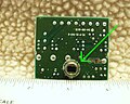 Rear of circuit board which faces mirror when in place. Pyroelectric sensor indicated by green arrow.
.JPG)


 Motion detector with superimposed beam pattern. The length of the beams is a measure of the detectors sensitivity in that direction.


