Search This Blog

Tuesday, August 8, 2023

Transmitter

From Wikipedia, the free encyclopedia
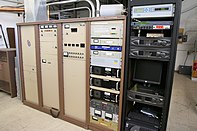
Commercial FM broadcasting transmitter at radio station WDET-FM, Wayne State University, Detroit, USA. It broadcasts at 101.9 MHz with a radiated power of 48 kW.

In electronics and telecommunications, a radio transmitter or just transmitter is an electronic device which produces radio waves with an antenna. The transmitter itself generates a radio frequency alternating current, which is applied to the antenna. When excited by this alternating current, the antenna radiates radio waves.

Transmitters are necessary component parts of all electronic devices that communicate by radio, such as radio and television broadcasting stations, cell phones, walkie-talkies, wireless computer networks, Bluetooth enabled devices, garage door openers, two-way radios in aircraft, ships, spacecraft, radar sets and navigational beacons. The term transmitter is usually limited to equipment that generates radio waves for communication purposes; or radiolocation, such as radar and navigational transmitters. Generators of radio waves for heating or industrial purposes, such as microwave ovens or diathermy equipment, are not usually called transmitters, even though they often have similar circuits.

The term is popularly used more specifically to refer to a broadcast transmitter, a transmitter used in broadcasting, as in FM radio transmitter or television transmitter. This usage typically includes both the transmitter proper, the antenna, and often the building it is housed in.

Description

A radio transmitter is usually part of a radio communication system which uses electromagnetic waves (radio waves) to transport information (in this case sound) over a distance.

A transmitter can be a separate piece of electronic equipment, or an electrical circuit within another electronic device. A transmitter and a receiver combined in one unit is called a transceiver. The term transmitter is often abbreviated "XMTR" or "TX" in technical documents. The purpose of most transmitters is radio communication of information over a distance. The information is provided to the transmitter in the form of an electronic signal called the modulation signal, such as an audio (sound) signal from a microphone, a video (TV) signal from a video camera, or in wireless networking devices, a digital signal from a computer. The transmitter generates a radio frequency signal which when applied to the antenna produces the radio waves, called the carrier signal. It combines the carrier with the modulation signal, a process called modulation. The information can be added to the carrier in several different ways, in different types of transmitters. In an amplitude modulation (AM) transmitter, the information is added to the radio signal by varying its amplitude. In a frequency modulation (FM) transmitter, it is added by varying the radio signal's frequency slightly. Many other types of modulation are also used.

The radio signal from the transmitter is applied to the antenna, which radiates the energy as radio waves. The antenna may be enclosed inside the case or attached to the outside of the transmitter, as in portable devices such as cell phones, walkie-talkies, and garage door openers. In more powerful transmitters, the antenna may be located on top of a building or on a separate tower, and connected to the transmitter by a feed line, that is a transmission line.

Radio transmitters
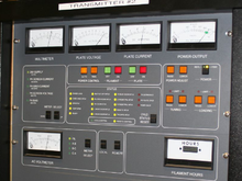
Elcom Bauer model 701B 1100 watt AM broadcast transmitter
 
35 kW, Continental 816R-5B FM transmitter, belonging to American FM radio station KWNR broadcasting on 95.5 MHz in Las Vegas
 
Modern amateur radio transceiver, the ICOM IC-746PRO. It can transmit on the amateur bands from 1.8 MHz to 144 MHz with an output power of 100 W
 
A CB radio transceiver in a truck, a two way radio transmitting on 27 MHz with a power of 4 W, that can be operated without a license
 
Consumer products that contain transmitters
 
A cellphone has several transmitters: a duplex cell transceiver, a Wi-Fi modem, and a Bluetooth modem.
 
Both the handset and the base of a cordless phone contain low power 2.4 GHz radio transmitters to communicate with each other.
 
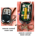
A garage door opener control contains a low-power 2.4 GHz transmitter that sends coded commands to the garage door mechanism to open or close.
 
A wireless microphone is a microphone with a low power FM transmitter which transmits the performer's voice to a nearby receiver connected to the sound system which amplifies the audio.
 
A laptop computer and home wireless router (background) which connects it to the Internet, creating a home Wi-Fi network. Both have Wi-Fi modems, automated microwave transmitters and receivers operating on 2.4 GHz which exchange data packets with the internet service provider (ISP).
 
A Bluetooth earbud with microphone. It has a Bluetooth modem to exchange audio with a cell phone

Operation

Animation of a half-wave dipole antenna transmitting radio waves, showing the electric field lines. The antenna in the center is two vertical metal rods, with an alternating current applied at its center from a radio transmitter (not shown). The voltage charges the two sides of the antenna alternately positive (+) and negative (−). Loops of electric field (black lines) leave the antenna and travel away at the speed of light; these are the radio waves. This animation shows the action slowed enormously

Electromagnetic waves are radiated by electric charges when they are accelerated. Radio waves, electromagnetic waves of radio frequency, are generated by time-varying electric currents, consisting of electrons flowing through a metal conductor called an antenna which are changing their velocity and thus accelerating. An alternating current flowing back and forth in an antenna will create an oscillating magnetic field around the conductor. The alternating voltage will also charge the ends of the conductor alternately positive and negative, creating an oscillating electric field around the conductor. If the frequency of the oscillations is high enough, in the radio frequency range above about 20 kHz, the oscillating coupled electric and magnetic fields will radiate away from the antenna into space as an electromagnetic wave, a radio wave.

A radio transmitter is an electronic circuit which transforms electric power from a power source, a battery or mains power, into a radio frequency alternating current to apply to the antenna, and the antenna radiates the energy from this current as radio waves. The transmitter also encodes information such as an audio or video signal into the radio frequency current to be carried by the radio waves. When they strike the antenna of a radio receiver, the waves excite similar (but less powerful) radio frequency currents in it. The radio receiver extracts the information from the received waves.

Components

A practical radio transmitter mainly consists of the following parts:

Many other types of modulation are also used. In large transmitters the oscillator and modulator together are often referred to as the exciter.
  • A radio frequency (RF) amplifier to increase the power of the signal, to increase the range of the radio waves.
  • An impedance matching (antenna tuner) circuit to transform the output impedance of the transmitter to match the impedance of the antenna (or the transmission line to the antenna), to transfer power efficiently to the antenna. If these impedances are not equal, it causes a condition called standing waves, in which the power is reflected back from the antenna toward the transmitter, wasting power and sometimes overheating the transmitter.

In higher frequency transmitters, in the UHF and microwave range, free running oscillators are unstable at the output frequency. Older designs used an oscillator at a lower frequency, which was multiplied by frequency multipliers to get a signal at the desired frequency. Modern designs more commonly use an oscillator at the operating frequency which is stabilized by phase locking to a very stable lower frequency reference, usually a crystal oscillator.

Regulation

Two radio transmitters in the same area that attempt to transmit on the same frequency will interfere with each other, causing garbled reception, so neither transmission may be received clearly. Interference with radio transmissions can not only have a large economic cost, it can be life-threatening (for example, in the case of interference with emergency communications or air traffic control).

For this reason, in most countries, use of transmitters is strictly controlled by law. Transmitters must be licensed by governments, under a variety of license classes depending on use such as broadcast, marine radio, Airband, Amateur and are restricted to certain frequencies and power levels. A body called the International Telecommunication Union (ITU) allocates the frequency bands in the radio spectrum to various classes of users. In some classes, each transmitter is given a unique call sign consisting of a string of letters and numbers which must be used as an identifier in transmissions. The operator of the transmitter usually must hold a government license, such as a general radiotelephone operator license, which is obtained by passing a test demonstrating adequate technical and legal knowledge of safe radio operation.

Exceptions to the above regulations allow the unlicensed use of low-power short-range transmitters in consumer products such as cell phones, cordless telephones, wireless microphones, walkie-talkies, Wi-Fi and Bluetooth devices, garage door openers, and baby monitors. In the US, these fall under Part 15 of the Federal Communications Commission (FCC) regulations. Although they can be operated without a license, these devices still generally must be type-approved before sale.

History

Hertz discovering radio waves in 1887 with his first primitive radio transmitter (background).

The first primitive radio transmitters (called spark gap transmitters) were built by German physicist Heinrich Hertz in 1887 during his pioneering investigations of radio waves. These generated radio waves by a high voltage spark between two conductors. Beginning in 1895, Guglielmo Marconi developed the first practical radio communication systems using these transmitters, and radio began to be used commercially around 1900. Spark transmitters could not transmit audio (sound) and instead transmitted information by radiotelegraphy: the operator tapped on a telegraph key which turned the transmitter on-and-off to produce radio wave pulses spelling out text messages in telegraphic code. At the receiver, these pulses were sometimes directly recorded on paper tapes, but more common was audble reception, which was translated back to text by an operator who knew the code. These spark-gap transmitters were used during the first three decades of radio (1887–1917), called the wireless telegraphy or "spark" era. Because they generated damped waves, spark transmitters were electrically "noisy". Their energy was spread over a broad band of frequencies, creating radio noise which interfered with other transmitters. Damped wave emissions were banned by international law in 1934.

Two short-lived competing transmitter technologies came into use after the turn of the century, which were the first continuous wave transmitters: the arc converter (Poulsen arc) in 1904 and the Alexanderson alternator around 1910, which were used into the 1920s.

All these early technologies were replaced by vacuum tube transmitters in the 1920s, which used the feedback oscillator invented by Edwin Armstrong and Alexander Meissner around 1912, based on the Audion (triode) vacuum tube invented by Lee De Forest in 1906. Vacuum tube transmitters were inexpensive and produced continuous waves, and could be easily modulated to transmit audio (sound) using amplitude modulation (AM). This made AM radio broadcasting possible, which began in about 1920. Practical frequency modulation (FM) transmission was invented by Edwin Armstrong in 1933, who showed that it was less vulnerable to noise and static than AM. The first FM radio station was licensed in 1937. Experimental television transmission had been conducted by radio stations since the late 1920s, but practical television broadcasting didn't begin until the late 1930s. The development of radar during World War II motivated the evolution of high frequency transmitters in the UHF and microwave ranges, using new active devices such as the magnetron, klystron, and traveling wave tube.

The invention of the transistor allowed the development in the 1960s of small portable transmitters such as wireless microphones, garage door openers and walkie-talkies. The development of the integrated circuit (IC) in the 1970s made possible the current proliferation of wireless devices, such as cell phones and Wi-Fi networks, in which integrated digital transmitters and receivers (wireless modems) in portable devices operate automatically, in the background, to exchange data with wireless networks.

The need to conserve bandwidth in the increasingly congested radio spectrum is driving the development of new types of transmitters such as spread spectrum, trunked radio systems and cognitive radio. A related trend has been an ongoing transition from analog to digital radio transmission methods. Digital modulation can have greater spectral efficiency than analog modulation; that is it can often transmit more information (data rate) in a given bandwidth than analog, using data compression algorithms. Other advantages of digital transmission are increased noise immunity, and greater flexibility and processing power of digital signal processing integrated circuits.

Nano-FTIR

From Wikipedia, the free encyclopedia
nano-FTIR schematics
The schematic representation of a nano-FTIR system with a broadband infrared source.

Nano-FTIR (nanoscale Fourier transform infrared spectroscopy) is a scanning probe technique that utilizes as a combination of two techniques: Fourier transform infrared spectroscopy (FTIR) and scattering-type scanning near-field optical microscopy (s-SNOM). As s-SNOM, nano-FTIR is based on atomic-force microscopy (AFM), where a sharp tip is illuminated by an external light source and the tip-scattered light (typically back-scattered) is detected as a function of tip position. A typical nano-FTIR setup thus consists of an atomic force microscope, a broadband infrared light source used for tip illumination, and a Michelson interferometer acting as Fourier-transform spectrometer. In nano-FTIR, the sample stage is placed in one of the interferometer arms, which allows for recording both amplitude and phase of the detected light (unlike conventional FTIR that normally does not yield phase information). Scanning the tip allows for performing hyperspectral imaging (i.e. complete spectrum at every pixel of the scanned area) with nanoscale spatial resolution determined by the tip apex size. The use of broadband infrared sources enables the acquisition of continuous spectra, which is a distinctive feature of nano-FTIR compared to s-SNOM. Nano-FTIR is capable of performing infrared (IR) spectroscopy of materials in ultrasmall quantities and with nanoscale spatial resolution. The detection of a single molecular complex and the sensitivity to a single monolayer has been shown. Recording infrared spectra as a function of position can be used for nanoscale mapping of the sample chemical composition, performing a local ultrafast IR spectroscopy and analyzing the nanoscale intermolecular coupling, among others. A spatial resolution of 10 nm to 20 nm is routinely achieved.

chemical ID with nano-FTIR
Nanoscale chemical identification with nano-FTIR: local spectroscopy performed by nano-FTIR allowed for chemical identification of a nanoscale contaminant – a Polydimethylsiloxane (PDMS) particle – adjacent to a Poly(methyl methacrylate) (PMMA) film.

For organic compounds, polymers, biological and other soft matter, nano-FTIR spectra can be directly compared to the standard FTIR databases, which allows for a straightforward chemical identification and characterization.

Nano-FTIR does not require special sample preparation and is typically performed under ambient conditions. It uses an AFM operated in noncontact mode that is intrinsically nondestructive and sufficiently gentle to be suitable for soft-matter and biological sample investigations. Nano-FTIR can be utilized from THz to visible spectral range (and not only in infrared as its name suggests) depending on the application requirements and availability of broadband sources. Nano-FTIR is complementary to tip-enhanced Raman spectroscopy (TERS), SNOM, AFM-IR and other scanning probe methods that are capable of performing vibrational analysis.

Basic principles

Principles of near-field probing
Principles of near-field probing: the sample is analyzed via scattering from a sharp, externally illuminated probe

Nano-FTIR is based on s-SNOM, where the infrared beam from a light source is focused onto a sharp, typically metalized AFM tip and the backscattering is detected. The tip greatly enhances the illuminating IR light in the nanoscopic volume around its apex, creating a strong near field. A sample, brought into this near field, interacts with the tip electromagnetically and modifies the tip (back)scattering in the process. Thus by detecting tip scattering, one can obtain information about the sample.

Nano-FTIR detects the tip-scattered light interferometrically. The sample stage is placed into one arm of a conventional Michelson interferometer, while a mirror on a piezo stage is placed into another, reference arm. Recording the backscattered signal while translating the reference mirror yields an interferogram. The subsequent Fourier transform of this interferogram returns the near-field spectra of the sample.

nano-FTIR and ATR FTIR
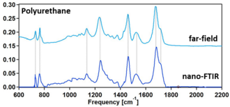
nano-FTIR absorption and far-field FTIR (ATR modality) spectra measured on the same polymer sample show great agreement.

Placement of the sample stage into one of the interferometer's arms (instead of outside of the interferometer as typically implemented in conventional FTIR) is a key element of nano-FTIR. It boosts the weak near-field signal due to interference with the strong reference field, helps to eliminate the background caused by parasitic scattering off everything that falls into large diffraction-limited beam focus, and most importantly, allows for recording of both amplitude s and phase φ spectra of the tip-scattered radiation. With the detection of phase, nano-FTIR provides complete information about near fields, which is essential for quantitative studies and many other applications. For example, for soft matter samples (organics, polymers, biomaterials, etc.), φ directly relates to the absorption in the sample material. This permits a direct comparison of nano-FTIR spectra with conventional absorption spectra of the sample material, thus allowing for simple spectroscopic identification according to standard FTIR databases.

History

Nano-FTIR was first described in 2005 in a patent by Ocelic and Hillenbrand as Fourier-transform spectroscopy of tip-scattered light with an asymmetric spectrometer (i.e. the tip/sample placed inside one of the interferometer arms). The first realization of s-SNOM with FTIR was demonstrated in 2006 in the laboratory of F. Keilmann using a mid-infrared source based on a simple version of nonlinear difference-frequency generation (DFG). However, the mid-IR spectra in this realization were recorded using dual comb spectroscopy principles, yielding a discrete set of frequencies and thus demonstrating a multiheterodyne imaging technique rather than nano-FTIR. The first continuous spectra were recorded only in 2009 in the same laboratory using a supercontinuum IR beam also obtained by DFG in GaSe upon superimposing two pulsed trains emitted from Er-doped fiber laser. This source further allowed in 2011 for the first assessment of nanoscale-resolved spectra of SiC with excellent quality and spectral resolution. At the same time, Huth et al. in the laboratory of R. Hillenbrand used IR radiation from a simple glowbar source in combination with the principles of Fourier-transform spectroscopy, to record IR spectra of p-doped Si and its oxides in a semiconductor device. In the same work the term nano-FTIR was first introduced. However, an insufficient spectral irradiance of glowbar sources limited the applicability of the technique to the detection of strongly-resonant excitations such phonons; and the early supercontinuum IR laser sources, while providing more power, had very narrow bandwidth (<300 cm−1). Further attempt to improve the spectral power, while retaining the large bandwidth of a glowbar source was made by utilizing the IR radiation from a high temperature argon arc source (also known as plasma source). However, due to lack of commercial availability and rapid development of the IR supercontinium laser sources, plasma sources are not widely utilized in nano-FTIR.

hyperspectral nano-FTIR image
Hyperspectral image of a copolymer blend acquired by nano-FTIR

The breakthrough in nano-FTIR came upon the development of high-power broadband mid-IR laser sources, which provided large spectral irradiance in a sufficiently large bandwidth (mW-level power in ~1000 cm-1 bandwidth) and enabled truly broadband nanoscale-resolved material spectroscopy capable of detecting even the weakest vibrational resonances. Particularly, it has been shown that nano-FTIR is capable of measuring molecular fingerprints which match well with far-field FTIR spectra, owing to the asymmetry of the nano-FTIR spectrometer that provides phase and thus gives access to the molecular absorption. Recently, the first nanoscale-resolved infrared hyperspectral imaging of a co-polymer blend was demonstrated, which allowed for the application of statistical techniques such as multivariate analysis – a widely used tool for heterogeneous sample analysis.

Additional boost to the development of nano-FTIR came from the utilization of the synchrotron radiation that provide extreme bandwidth, yet at the expense of weaker IR spectral irradiance compared to broadband laser sources.

Commercialization

Nano-FTIR integrated with s-SNOM (neaSNOM)
Nano-FTIR integrated with s-SNOM (neaSNOM) with all three base components marked by arrows.

The nano-FTIR technology has been commercialized by neaspec – a Germany-based spin-off company of the Max Planck Institute of Biochemistry founded by Ocelic, Hillenbrand and Keilmann in 2007 and based on the original patent by Ocelic and Hillenbrand. The detection module optimized for broadband illumination sources was first made available in 2010 as a part of the standard neaSNOM microscope system. At this time, broadband IR-lasers have not been yet commercially available, however experimental broadband IR-lasers prove that the technology works perfect and that it has a huge application potential across many disciplines. The first nano-FTIR was commercially available in 2012 (supplied with still experimental broadband IR-laser sources), becoming the first commercial system for broadband infrared nano-spectroscopy. In 2015 neaspec develops and introduces Ultrafast nano-FTIR, the commercial version of ultrafast nano-spectroscopy. Ultrafast nano-FTIR is a ready-to-use upgrade for nano-FTIR to enable pump-probe nano-spectroscopy at best-in-class spatial resolution. The same year the development of a cryo-neaSNOM – the first system of its kind to enable nanoscale near-field imaging & spectroscopy at cryogenic temperatures – was announced.

Advanced capabilities

Synchrotron beamlines integration

Nano-FTIR systems can be easily integrated into synchrotron radiation beamlines. The use of synchrotron radiation allows for acquisition of an entire mid-infrared spectrum at once. Synchrotrons radiation has already been utilized in synchrotron infrared microscopectroscopy - the technique most widely used in biosciences, providing information on chemistry on microscales of virtually all biological specimens, like bone, plants, and other biological tissues. Nano-FTIR brings the spatial resolution to 10-20 nm scale (vs. ~2-5 μm in microspectroscopy), which has been utilized for broadband spatially-resolved spectroscopy of crystalline and phase-change materials, semiconductors, minerals, biominerals and proteins.

Ultrafast spectroscopy

Nano-FTIR is highly suitable for performing local ultrafast pump-probe spectroscopy due to intereferometric detection and an intrinsic ability to vary the probe delay time. It has been applied for studies of ultrafast nanoscale plasmonic phenomena in Graphene, for performing nanospectroscopy of InAs nanowires with subcycle resolution and for probing the coherent vibrational dynamics of nanoscopic ensembles.

Quantitative studies

The availability of both amplitude and phase of the scattered field and theoretically well understood signal formation in nano-FTIR allow for the recovery of both real and imaginary parts of the dielectric function, i.e. finding the index of refraction and the extinction coefficient of the sample. While such recovery for arbitrarily-shaped samples or samples exhibiting collective excitations, such as phonons, requires a resource-demanding numerical optimization, for soft matter samples (polymers, biological matter and other organic materials) the recovery of the dielectric function could often be performed in real time using fast semi-analytical approaches. One of such approaches is based on the Taylor expansion of the scattered field with respect to a small parameter that isolates the dielectric properties of the sample and allows for a polynomial representation of measured near-field contrast. With an adequate tip-sample interaction model and with known measurement parameters (e.g. tapping amplitude, demodulation order, reference material, etc.), the sample permittivity can be determined as a solution of a simple polynomial equation.

Subsurface analysis

Near-field methods, including nano-FTIR, are typically viewed as a technique for surface studies due to short probing ranges of about couple tip radii (~20-50 nm). However it has been demonstrated that within such probing ranges, s-SNOM is capable of detecting subsurface features to some extents, which could be used for the investigations of samples capped by thin protective layers, or buried polymers, among others.

As a direct consequence of being quantitative technique (i.e. capable of highly reproducible detection of both near-field amplitude & phase and well understood near-field interaction models), nano-FTIR also provides means for the quantitative studies of the sample interior (within the probing range of the tip near field, of course). This is often achieved by a simple method of utilizing signals recorded at multiple demodulation orders naturally returned by nano-FTIR in the process of background suppression. It has been shown that higher harmonics probe smaller volumes below the tip, thus encoding the volumetric structure of a sample. This way, nano-FTIR has a demonstrated capability for the recovery of thickness and permittivity of layered films and nanostructures, which has been utilized for the nanoscale depth profiling of multiphase materials and high-Tc cuprate nanoconstriction devices patterned by focused ion beams. In other words, nano-FTIR has a unique capability of recovering the same information about thin-film samples that is typically returned by ellipsometry or impedance spectroscopy, yet with nanoscale spatial resolution. This capability proved crucial for disentangling different surface states in topological insulators.

Operation in liquid

Nano-FTIR uses scattered IR light to obtain information about the sample and has the potential to investigate electrochemical interfaces in-situ/operando and biological (or other) samples in their natural environment, such as water. The feasibility of such investigations has already been demonstrated by acquisition of nano-FTIR spectra through a capping Graphene layer on top of a supported material or through Graphene suspended on a perforated silicon nitride membrane (using the same s-SNOM platform that nano-FTIR utilizes).

Cryogenic environment

Reveling the fundamentals of phase transitions in superconductors, correlated oxides, Bose-Einstein condensates of surface polaritons, etc. require spectroscopic studies at the characteristically nanometer length scales and in cryogenic environment. Nano-FTIR is compatible with cryogenic s-SNOM that has already been utilized for reveling a nanotextured coexistence of metal and correlated Mott insulator phases in Vanadium oxide near the metal-insulator transition.

Special atmosphere environments

Nano-FTIR can be operated in different atmospheric environments by enclosing the system into an isolated chamber or a glove box. Such operation has already been used for the investigation of highly reactive Lithium-ion battery components.

Applications

Nano-FTIR has a plenitude of applications, including polymers and polymer composites, organic films, semiconductors, biological research (cell membranes, proteins structure, studies of single viruses), chemistry and catalysis, photochemistry, minerals and biominerals, geochemistry, corrosion and materials sciences, low-dimensional materials, photonics, energy storage, cosmetics, pharmacology and environmental sciences.

Materials and chemical sciences

Nano-FTIR has been used for the nanoscale spectroscopic chemical identification of polymers and nanocomposites, for in situ investigation of structure and crystallinity of organic thin films, for strain characterization and relaxation in crystalline materials and for high-resolution spatial mapping of catalytic reactions, among others.

Biological and pharmaceutical sciences

Nano-FTIR has been used for investigation of protein secondary structure, bacterial membrane, detection and studies of single viruses and protein complexes. It has been applied to the detection of biominerals in bone tissue. Nano-FTIR, when coupled with THz light, can also be applied to cancer and burn imaging with high optical contrast.

Semiconductor industry and research

Nano-FTIR has been used for nanoscale free carrier profiling and quantification of free carrier concentration in semiconductor devices, for evaluation of ion beam damage in nanoconstriction devices, and general spectroscopic characterization of semiconductor materials.

Theory

High-harmonic demodulation for background suppression

The nano-FTIR interferometrically detects light scattered from the tip-sample system, . The power at the detector can be written as

where is the reference field. The scattered field can be written as

and is dominated by parasitic background scattering, , from the tip shaft, cantilever sample roughness and everything else which falls into the diffraction-limited beam focus. To extract the near-field signal, , originating from the "hot-spot" below the tip apex (which carries the nanoscale-resolved information about the sample properties) a small harmonic modulation of the tip height H (i.e. oscillating the tip) with frequency Ω is provided and the detector signal is demodulated at higher harmonics of this frequency nΩ with n=1,2,3,4,... The background is nearly insensitive to small variations of the tip height and is nearly eliminated for sufficiently high demodulation orders (typically ). Mathematically this can be shown by expanding and into a Fourier series, which yields the following (approximated) expression for the demodulated detector signal:

where is the complex-valued number that is obtained by combining the lock-in amplitude, , and phase, , signals, is the n-th Fourier coefficient of the near-field contribution and C. C. stands for the complex conjugate terms. is the zeroth-order Fourier coefficient of the background contribution and is often called the multiplicative background because it enters the detector signal as a product with . It cannot be removed by the high-harmonic demodulation alone. In nano-FTIR the multiplicative background is eliminated as described below.

Asymmetric FTIR spectrometer

To acquire a spectrum, the reference mirror is continuously translated while recording the demodulated detector signal as a function of the reference mirror position , yielding an interferogram . This way the phase of the reference field changes according to for each spectral component of the reference field and the detector signal can thus be written as

where is the reference field at zero delay . To obtain the nano-FTIR spectrum, , the interferogram is Fourier-transformed with respect to . The second term in the above equation does not depend on the reference mirror position and after the Fourier transformation contributes only to the DC signal. Thus for only the near-field contribution multiplied by the reference field stays in the acquired spectrum:

This way, besides providing the interferometric gain, the asymmetric interferometer utilized in nano-FTIR also eliminates the multiplicative background, which otherwise could be a source of various artifacts and is often overlooked in other s-SNOM based spectroscopies.

Normalization

Following the standard FTIR practice, spectra in nano-FTIR are normalized to those obtained on a known, preferably spectrally-flat reference material. This eliminates the generally unknown reference field and any instrumental functions, yielding spectra of the near-field contrast:

Near-field contrast spectra are generally complex-valued, reflecting on the possible phase delay of the sample-scattered field with respect to the reference. Near-field contrast spectra depend nearly exclusively on the dielectric properties of sample material and can be used for its identification and characterization.

Nano-FTIR absorption spectroscopy

For the purpose of describing near-field contrasts for optically thin samples composed of polymers, organics, biological matter and other soft matter (so called weak oscillators), the near-field signal to a good approximation can be expressed as:

,

where is the surface response function that depends on the complex-valued dielectric function of the sample and can be also viewed as the reflection coefficient for evanescent waves that constitute the near field of the tip. That is, the spectral dependence of is determined exclusively by the sample reflection coefficient. The latter is purely real and acquires an imaginary part only in narrow spectral regions around the sample absorption lines. This means that the spectrum of an imaginary part of the near-field contrast resembles the conventional FTIR absorbance spectrum, , of the sample material:. It is therefore convenient to define the nano-FTIR absorption , which directly relates to the sample absorbance spectrum:

It can be used for direct sample identification and characterization according to the standard FTIR databases without the need of modeling the tip-sample interaction.

For phononic and plasmonic samples in the vicinity of the corresponding surface surface resonances, the relation might not hold. In such cases the simple relation between and can not be obtained, requiring modeling of the tip-sample interaction for spectroscopic identification of such samples.

Analytical and numerical simulations

Significant efforts have been put towards simulating nano-FTIR electric field and complex scattering signal through numerical methods (using commercial proprietary software such as CST Microwave Studio, Lumerical FDTD, and COMSOL Multiphysics) as well as through analytical models (such as through finite dipole and point dipole approximations). Analytical simulations tend to be more simplified and inaccurate, while numerical methods are more rigorous but computationally expensive.

Politics of Europe

From Wikipedia, the free encyclopedia ...