The nanoscopic scale (or nanoscale) usually refers to structures with a length scale applicable to nanotechnology, usually cited as 1–100 nanometers (nm). A nanometer is a billionth of a meter. The nanoscopic scale is (roughly speaking) a lower bound to the mesoscopic scale for most solids.
For technical purposes, the nanoscopic scale is the size at which
fluctuations in the averaged properties (due to the motion and behavior
of individual particles) begin to have a significant effect (often a
few percent) on the behavior of a system, and must be taken into account
in its analysis.
The nanoscopic scale is sometimes marked as the point where the
properties of a material change; above this point, the properties of a
material are caused by 'bulk' or 'volume' effects, namely which atoms
are present, how they are bonded, and in what ratios. Below this point,
the properties of a material change, and while the type of atoms present
and their relative orientations are still important, 'surface area
effects' (also referred to as quantum effects)
become more apparent – these effects are due to the geometry of the
material (how thick it is, how wide it is, etc.), which, at these low
dimensions, can have a drastic effect on quantized states, and thus the
properties of a material.
Nanotechnology, often shortened to nanotech, is the use of matter on atomic, molecular, and supramolecular
scales for industrial purposes. The earliest, widespread description of
nanotechnology referred to the particular technological goal of
precisely manipulating atoms and molecules for fabrication of macroscale
products, also now referred to as molecular nanotechnology. A more generalized description of nanotechnology was subsequently established by the National Nanotechnology Initiative, which defined nanotechnology as the manipulation of matter with at least one dimension sized from 1 to 100 nanometers (nm). This definition reflects the fact that quantum mechanical effects are important at this quantum-realm
scale, and so the definition shifted from a particular technological
goal to a research category inclusive of all types of research and
technologies that deal with the special properties of matter which occur
below the given size threshold. It is therefore common to see the
plural form "nanotechnologies" as well as "nanoscale technologies" to refer to the broad range of research and applications whose common trait is size.
Scientists currently debate the future implications of nanotechnology. Nanotechnology may be able to create many new materials and devices with a vast range of applications, such as in nanomedicine, nanoelectronics, biomaterials
energy production, and consumer products. On the other hand,
nanotechnology raises many of the same issues as any new technology,
including concerns about the toxicity and environmental impact of nanomaterials, and their potential effects on global economics, as well as speculation about various doomsday scenarios. These concerns have led to a debate among advocacy groups and governments on whether special regulation of nanotechnology is warranted.
Nanomachines
Molecular machines
are a class of molecules typically described as an assembly of a
discrete number of molecular components intended to produce mechanical
movements in response to specific stimuli, mimicking macromolecular
devices such as switches and motors. Naturally occurring or biological
molecular machines are responsible for vital living processes such as DNA replication and ATP synthesis. Kinesins and ribosomes are examples of molecular machines, and they often take the form of multi-protein complexes.
For the last several decades, scientists have attempted, with varying
degrees of success, to miniaturize machines found in the macroscopic
world. The first example of an artificial molecular machine (AMM) was
reported in 1994, featuring a rotaxane with a ring and two different possible binding sites.Kinesin walking on a microtubule is a molecular biological machine using protein domain dynamics on nanoscales. In 2016 the Nobel Prize in Chemistry was awarded to Jean-Pierre Sauvage, Sir J. Fraser Stoddart, and Bernard L. Feringa for the design and synthesis of molecular machines.
AMMs have diversified rapidly over the past few decades and their design principles, properties, and characterization
methods have been outlined better. A major starting point for the
design of AMMs is to exploit the existing modes of motion in molecules,
such as rotation about single bonds or cis-trans isomerization. Different AMMs are produced by introducing various functionalities, such as the introduction of bistability
to create switches. A broad range of AMMs has been designed, featuring
different properties and applications; some of these include molecular motors, switches, and logic gates. A wide range of applications have been demonstrated for AMMs, including those integrated into polymeric, liquid crystal, and crystalline systems for varied functions (such as materials research, homogenous catalysis and surface chemistry).
Functionalities can be added to nanomaterials by interfacing them
with biological molecules or structures. The size of nanomaterials is
similar to that of most biological molecules and structures; therefore,
nanomaterials can be useful for both in vivo and in vitro biomedical
research and applications. Thus far, the integration of nanomaterials
with biology has led to the development of diagnostic devices, contrast
agents, analytical tools, physical therapy applications, and drug
delivery vehicles.
Nanomedicine seeks to deliver a valuable set of research tools and clinically useful devices in the near future. The National Nanotechnology Initiative expects new commercial applications in the pharmaceutical industry that may include advanced drug delivery systems, new therapies, and in vivo imaging. Nanomedicine research is receiving funding from the US National Institutes of Health Common Fund program, supporting four nanomedicine development centers.
Nanomedicine sales reached $16 billion in 2015, with a minimum of $3.8
billion in nanotechnology R&D being invested every year. Global
funding for emerging nanotechnology increased by 45% per year in recent
years, with product sales exceeding $1 trillion in 2013. As the nanomedicine industry continues to grow, it is expected to have a significant impact on the economy.
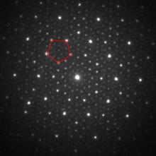
Figure 1: Selected area diffraction pattern of a twinned austenite crystal in a piece of steel
Electron diffraction refers to changes in the direction of electron beams due to interactions with atoms. Close to the atoms the changes are described as Fresnel diffraction; far away they are called Fraunhofer diffraction. The resulting map of the directions of the electrons far from the sample (Fraunhofer diffraction) is called a diffraction pattern, see for instance Figure 1. These patterns are similar to x-ray and neutron diffraction
patterns, and are used to study the atomic structure of gases, liquids,
surfaces and bulk solids. Electron diffraction also plays a major role
in the contrast of images in electron microscopes.
Electron diffraction occurs due to elastic scattering, when there is no change in the energy of the electrons during their interactions with atoms. The negatively charged electrons are scattered due to Coulomb forces
when they interact with both the positively charged atomic core and the
negatively charged electrons around the atoms; most of the interaction
occurs quite close to the atoms, within about one angstrom. In comparison, x-rays are scattered after interactions with the electron density while neutrons are scattered by the atomic nuclei through the strong nuclear force.
Description
All matter can be thought of as matter waves,
from small particles such as electrons up to macroscopic objects –
although it is impossible to measure any of the "wave-like" behavior of
macroscopic objects. Waves can move around objects and create
interference patterns, and a classic example is the Young's two-slit experiment shown in Figure 2,
where a wave impinges upon two slits in the first of the two images.
After going through the slits there are directions where the wave is
stronger, ones where it is weaker – the wave has been diffracted.
If instead of two slits there are a number of small points then similar
phenomena can occur as shown in the second image where the wave is
coming in from the bottom right corner. This is comparable to
diffraction of an electron wave where the small dots would be atoms, see also note.
Close to the aperture or atoms, often called the "sample", the electron wave would be described in terms of near field or Fresnel diffraction. This has relevance for imaging within electron microscopes,whereas electron diffraction patterns are measured far from the sample, which is described as far-field or Fraunhofer diffraction. A map of the directions of the electron waves
leaving the sample will show high intensity (white) for favored
directions, such as the three prominent ones in the Young's slits
experiment of Figure 2, while the other directions will be low intensity (dark). Often there will be an array of spots (preferred directions) as in Figure 1 and the other figures shown later.
Figure 2: The first is the Young's slit experiment, with the second similar from a small array of atoms.
Strictly, the term electron diffraction refers to how electrons are
scattered by atoms, a process that is mathematically modelled by solving
forms of Schrödinger equation.
However, it is often also used to denote, collectively, different
methods of collecting data on the directions of electrons leaving the
sample, what are better called electron diffraction patterns. The normal
usage in the field
is to collectively refer to both the scattering process and the maps of
directions as electron diffraction, not differentiating the two.
Therefore, strictly, electron diffraction also plays a major role in how
images are formed in different types of electron microscope such as transmission, scanning transmission, scanning and low-energy.
Most of this document will describe electron diffraction in terms of
different types of electron diffraction patterns, with less emphasis on
the scattering processes beyond providing some citations and general
discussion; for imaging see the pages linked above.
The most common use of electron diffraction patterns is in transmission electron microscopy (TEM) with thin samples of tens to at most a thousand atoms in thickness, that is 1 nanometer
to 100 nanometers. Some details on methods for sample preparation of
thin samples can be found in the book by Jeffrey Williams Edington, within journal publications, in the unpublished literature and within the page transmission electron microscopy. There are many different ways to collect diffraction information in a TEM such as selected area, convergent beam, precession and 4D STEM as described below. There are also many other types of instruments. For instance, in scanning electron microscopy (SEM), electron backscatter diffraction
is used to determine crystal orientation across the sample. Electron
diffraction patterns can further be used to characterize molecules using
gas electron diffraction, surfaces using lower energy electrons, a technique called LEED, and by reflecting electrons off surfaces, a technique called RHEED, see later.
There are many levels of analysis and explanation of the
theoretical basis of electron diffraction, elements of which are
described later. These include:
The simplest approximation using the de Broglie wavelength for electrons, where only the geometry is considered and often Bragg's law is invoked, a far-field or Fraunhofer approach.
The first level of more accuracy where it is approximated that the electrons are only scattered once, which is called kinematical diffraction and is also a far-field or Fraunhofer approach.
More complete and accurate explanations where multiple scattering is included, what is called dynamical diffraction (e.g. refs). These involve more general analyses using relativistically corrected Schrödinger equation methods.
Unlike x-ray diffraction and neutron diffraction
where the simplest approximations are quite accurate, with electron
diffraction this is not the case. Simple models give the geometry of the
intensities in a diffraction pattern, but higher level ones cited above
and later are needed for many details and the intensities – numbers
matter.
History
The
historical background is divided into several subsections. The first is
the general background to electrons in vacuum and the technological
developments that led to cathode-ray tubes as well as vacuum tubes
that dominated early television and electronics; the second is how
these led to the development of electron microscopes; the last is work
on the nature of electron beams and the fundamentals of how electrons
behave, a key component of quantum mechanics and the explanation of electron diffraction.
Figure 3 A Crookes tube – without emission (top) and with emission and a shadow due to the maltese cross blocking part of the electron beam (bottom); see also cathode ray tube
Experiments involving electron beams occurred long before the discovery of the electron; indeed, the name ēlektron comes from the Greek word for amber, which in turn is connected to the recording of electrostatic charging by Thales of Miletus around 585 BCE, and possibly others even earlier.
In 1650, Otto von Guericke invented the vacuum pump allowing for study of the effects of high voltage electricity passing through rarefied air. In 1838, Michael Faraday applied a high voltage between two metal electrodes
at either end of a glass tube that had been partially evacuated of air,
and noticed a strange light arc with its beginning at the cathode (negative electrode) and its end at the anode (positive electrode). Building on this In the 1850's, Heinrich Geissler was able to achieve a pressure of around 10−3atmospheres, inventing what became known as Geissler tubes. Using these tubes, while studying electrical conductivity in rarefied gases in 1859 Julius Plücker
observed that the radiation emitted from the negatively charged cathode
caused phosphorescent light to appear on the tube wall near it, and the
region of the phosphorescent light could be moved by application of a
magnetic field.
In 1869, Plücker's student Johann Wilhelm Hittorf found that a solid body placed between the cathode and the phosphorescence would cast a shadow on the tube, e,g, Figure 3.
Hittorf inferred that there are straight rays emitted from the cathode
and that the phosphorescence was caused by the rays striking the tube
walls. In 1876 Eugen Goldstein showed that the rays were emitted perpendicular to the cathode surface, which distinguished them from the incandescent light. Eugen Goldstein dubbed them cathode rays. By the 1870s William Crookes and others were able to evacuate glass tubes below 10−6
atmospheres, and observed that the glow in the whole tube disappeared
when the pressure was reduced but the glass behind the anode began to
glow. Crookes was also able to show that the particles in the cathode
rays were negatively charged and could be deflected by an
electromagnetic field.
In 1897, Joseph Thomson measured the mass of these cathode rays,
proving they were made of particles. These particles, however, were
1800 times lighter than the lightest particle known at that time – a hydrogen atom. These were originally called corpuscle and later named the electron by George Johnstone Stoney.
The control of electron beams that this work led to resulted in
significant technology advances in electronic amplifiers and television
displays.
Figure 4: Propagation of a wave packet demonstrating the movement of a bundle of waves; see group velocity for more details.
Independent of the developments for electrons in vacuum, at about the
same time the components of quantum mechanics were being assembled. In
1924 Louis de Broglie in his PhD thesis Recherches sur la théorie des quanta introduced his theory of electron waves. He suggested that an electron around a nucleus could be thought of as being a standing wave,
and that electrons and all matter could be considered as waves. He
merged the idea of thinking about them as particles (or corpuscles), and
of thinking of them as waves. He proposed that particles are bundles of
waves (wave packets) which move with a group velocity and have an effective mass, see for instance Figure 4. Both of these depend upon the energy, which in turn connects to the wavevector and the relativistic formulation of Albert Einstein a few years before.
This rapidly became part of what was called by Erwin Schrödingerundulatory mechanics, now called the Schrödinger equation or wave mechanics. As stated by Louis de Broglie on September 8th 1927 in the preface to the German translation of his theses (in turn translated into English):
M. Einstein from the beginning has supported my thesis, but it was M. E. Schrödinger
who developed the propagation equations of a new theory and who in
searching for its solutions has established what has become known as
“Wave Mechanics”.
The Schrödinger equation combines the kinetic energy of waves and the potential energy due to, for electrons, the Coulomb potential. He was able to explain earlier work such as the quantization of the energy of electrons around atoms in the Bohr model,
as well as many other phenomena. Electron waves as hypothesized by de
Broglie were automatically part of the solutions to his equation, see
also introduction to quantum mechanics and matter waves.
Both the wave nature and the undulatory mechanics approach were
experimentally confirmed for electron beams by experiments from two
groups performed independently, the first the Davisson–Germer experiment, the other by George Paget Thomson and Alexander Reid; see note for more discussion. Alexander Reid, who was Thomson's graduate student, performed the first experiments, but he died soon after in a motorcycle accident
and is rarely mentioned. These experiments were rapidly followed by the
first non-relativistic diffraction model for electrons by Hans Bethe based upon the Schrödinger equation, which is very close to how electron diffraction is now described. Significantly, Davidsson and Germer noticed that their results could not be interpreted using a Bragg's law approach as the positions were systematically different; the approach of Bethe
which includes the refraction due to the average potential yielded more
accurate results. These advances in understanding of electron wave
mechanics were important for many developments of electron-based
analytical techniques in the 1930s such as gas electron diffraction developed by Herman Mark and Raymond Weil, and the first electron microscopes developed by Max Knoll and Ernst Ruska.
Electron microscopes and early electron diffraction
Just having an electron beam was not enough, it needed to be controlled. Many developments laid the groundwork of electron optics; see the paper by Calbick for an overview of the early work. One significant step was the work of Hertz in 1883
who made a cathode-ray tube with electrostatic and magnetic deflection,
demonstrating manipulation of the direction of an electron beam. Others
were focusing of the electrons by an axial magnetic field by Emil Wiechert in 1899, improved oxide-coated cathodes which produced more electrons by Arthur Wehnelt in 1905 and the development of the electromagnetic lens in 1926 by Hans Busch.
Figure 5: Replica built in 1980 by Ernst Ruska of the original electron microscope, in the Deutsches Museum in Munich
Building an electron microscope involves combining these elements, similar to a optical microscope
but with magnetic or electrostatic lenses instead of glass ones. To
this day the issue of who invented the transmission electron microscope
is controversial, as discussed by T. Mulvey and more recently by Tao. Extensive additional information can be found in the articles by M. M. Freundlich, Reinhold Rüdenberg and Mulvey.
One effort was university based. In 1928, at the Technical University of Berlin, Adolf Matthias (Professor of High Voltage Technology and Electrical Installations) appointed Max Knoll
to lead a team of researchers to advance research on electron beams and
cathode-ray oscilloscopes. The team consisted of several PhD students
including Ernst Ruska. In 1931, Max Knoll and Ernst Ruska
successfully generated magnified images of mesh grids placed over an
anode aperture. The device, a replicate of which is shown in Figure 5, used two magnetic lenses to achieve higher magnifications, the first electron microscope. (Max Knoll died in 1969, so did not receive a share of the Nobel Prize in 1986.)
Apparently independent of this effort was work at Siemens-Schuckert by Reinhold Rüdenberg. According to patent law (U.S. Patent No. 2058914 and 2070318,
both filed in 1932), he is the inventor of the electron microscope, but
it is not clear when he had a working instrument. He stated in a very
brief article in 1932
that Siemens had been working on this for some years before the patents
were filed in 1932, so his effort was parallel to the university
effort. He died in 1961, so similar to Max Knoll, was not eligible for a
share of the Nobel Prize.
These instruments could produce magnified images, but were not
particularly useful for electron diffraction; indeed, the wave nature of
electrons was not exploited during the development. Key for electron
diffraction in microscopes was the advance in 1936 where Boersch showed
that they could be used as micro-diffraction cameras with an aperture -- the birth of selected area electron diffraction.
Less controversial was the development of low-energy electron diffraction -- the early experiments of Davisson and Germer used this approach. As early as 1929 Germer investigated gas adsorption, and in 1932 Farnsworth probed single crystals of copper and silver.
However, the vacuum systems available at that time was not good enough
to properly control the surfaces, and it took almost forty years before
these became available. Similarly, it was not until about 1965 that Sewell and Cohen demonstrated the power of reflection high-energy electron diffraction in a system with a very well controlled vacuum.
Further developments
Despite early successes such as the determination of the positions of hydrogen atoms in NH4Cl crystals by Laschkarew and Usykin in 1933, boric acid by Cowley in 1953 and orthoboric acid by Zachariasen in 1954, electron diffraction for many years was a qualitative technique used to check samples within electron microscopes. John M Cowley explains in a 1968 paper:
Thus
was founded the belief, amounting in some cases almost to an article of
faith, and persisting even to the present day, that it is impossible to
interpret the intensities of electron diffraction patterns to gain
structural information.
This has changed, in transmission, reflection and at low energies. Some of the key developments have been:
Fast numerical methods based upon the Cowley-Moodie multislice algorithm, which only became possible once the fast Fourier transform (FFT) method was developed. With these and other numerical methods it became possible to calculate accurate, dynamical diffraction in seconds to minutes with laptops using widely available multislice programs.
Developments in the convergent-beam electron diffraction approach. Building on the original work of Kossel and Möllenstedt in 1939, it was extended by Goodman and Lehmpfuh, then mainly by the groups of Steeds and Tanaka who showed how to determine point groups and space groups. It can also be used for higher-level refinements of the electron density; for a brief history see CBED history. In many cases this is the best method to determine symmetry.
The development of new approaches to reduce dynamical effects such as precession electron diffraction
and three-dimensional diffraction methods. Averaging over different
directions has, empirically, been found to significantly reduce
dynamical diffraction effects, e.g. See PED history
for further details. Not only is it easier to identify known structures
with this approach, it can also be used to solve unknown structures in
some cases – see precession electron diffraction for further information.
The development of experimental methods exploiting ultra-high vacuum technologies (e.g. the approach described by Alpert in 1953) to better control surfaces, making low-energy electron diffraction and reflection high-energy electron diffraction
more reliable and reproducible techniques. In the early days the
surfaces were not well controlled; with these technologies they can both
be cleaned and remain clean for hours to days, a key component of surface science.
Fast and accurate methods to calculate intensities for low-energy electron diffraction so it could be used to determine atomic positions, for instance references.
These have been extensively exploited to determine the structure of
many surfaces, and the arrangement of foreign atoms on surfaces.
Methods to simulate the intensities in reflection high-energy electron diffraction, so it can be used semi-quantitatively to understand surfaces during growth and thereby to control the resulting materials.
The development of advanced detectors for transmission electron microscopy such as charge-coupled device or direct electron detectors,
improving the accuracy and reliability of intensity measurements. These
have efficiencies and accuracies that can be a thousand or more times
that of the photographic film used in the earliest experiments, with the information available in real time rather than requiring photographic processing after the experiment.
Basics
Geometrical considerations
What
is seen in an electron diffraction pattern depends upon the sample and
also the energy of the electrons. The electrons need to be considered as
waves, which involves describing the electron via a wavefunction,
written in crystallographic notation as:
for a position . This is a quantum mechanics description; one cannot use a classical approach. The vector is called the wavevector, has units of inverse nanometers, and the form above is called a plane wave as the term inside the exponential is constant on the surface of a plane. The vector is also what is used when drawing ray diagrams.
For most cases the electrons are travelling at a respectable
fraction of the speed of light, so rigorously need to be considered
using relativistic quantum mechanics via the Dirac equation, which as spin does not normally matter can be reduced to the Klein–Gordon equation. Fortunately one can side-step many complications and use a non-relativistic approach based around the Schrödinger equation. Following Kunio Fujiwara and Archibald Howie, the relationship between the total energy of the electrons and the wavevector is written as:
with
where is Planck's constant, is a relativistic effective mass used to cancel out the relativistic terms for electrons of energy with the speed of light and the rest mass of the electron. The concept of effective mass occurs throughout physics (see for instance Ashcroft and Mermin), and comes up in the behavior of quasiparticles. A common one is the electron hole,
which acts as if it is a particle with a positive charge and a mass
similar to that of an electron, although it can be several times lighter
or heavier. For electron diffraction the electrons behave as if they
are non-relativistic particles of mass in terms of how they interact with the atoms.
The wavelength of the electrons in vacuum is
and can range from about 0.1 nanometers, roughly the size of an atom, down to a thousandth of that. Typically the energy of the electrons is written in electronvolts (eV), the voltage used to accelerate the electrons; the actual energy of each electron is this voltage times the electron charge. For context, the typical energy of a chemical bond is a few eV; electron diffraction involves electrons up to 5,000,000 eV.
The magnitude of the interaction of the electrons with a material scales as
While the wavevector increases as the energy increases, the change in the effective mass compensates this so even at the very high energies used in electron diffraction there are still significant interactions.[82]
The high-energy electrons interact with the Coulomb potential, which for a crystal can be considered in terms of a Fourier series (see for instance Ashcroft and Mermin), that is
with a reciprocal lattice vector and the corresponding Fourier coefficient of the potential. The reciprocal lattice vector is often referred to in terms of Miller indices, a sum of the individual reciprocal lattice vectors with integers in the form:
(Sometimes reciprocal lattice vectors are written as , , and see note.) The contribution from the needs to be combined with what is called the shape function (e.g.), which is the Fourier transform
of the shape of the object. If, for instance, the object is small in
one dimension then the shape function extends far in that direction in
the Fourier transform—a reciprocal relationship.
Figure 6: Ewald sphere construction for transmission electron diffraction, showing two of the Laue zones and the excitation error
Around each reciprocal lattice point one has this shape function. How much intensity there will be in the diffraction pattern depends upon the intersection of the Ewald sphere, that is energy conservation, and the shape function around each reciprocal lattice point -- see Figures 6, 20 and 22. The vector from a reciprocal lattice point to the Ewald sphere is called the excitation error.
For transmission electron diffraction the samples used are thin, so
most of the shape function is along the direction of the electron beam.
For both LEED and RHEED the shape function is mainly normal to the surface of the sample. In LEED this results in (a simplification) back-reflection of the electrons leading to spots, see Figures 20 and 21 later, whereas in RHEED the electrons reflect off the surface at a small angle and typically yield diffraction patterns with streaks, see Figures 22 and 23
later. By comparison, with both x-ray and neutron diffraction the
scattering is significantly weaker, so typically requires much larger
crystals, in which case the shape function shrinks to just around the
reciprocal lattice points, leading to simpler Bragg's law diffraction.
For all cases, when the reciprocal lattice points are close to
the Ewald sphere (the excitation error is small) the intensity tends to
be higher; when they are far away it tends to be smaller. The set of
diffractions spots at right angles to the direction of the incident beam
are called the zero-order Laue zone (ZOLZ) spots, as shown in Figure 6.
One can also have intensities further out from reciprocal lattice
points which are in a higher layer. The first of these is called the
first order Laue zone (FOLZ); the series is called by the generic name
higher order Laue zone (HOLZ).
The end result is that the electron wave after it has been diffracted can be written as a integral over different plane waves:
that is a sum of plane waves going in different directions, each with a complex amplitude . (This is a three dimensional integral, which is often written as rather than .) For a crystalline sample these wavevectors have to be of the same magnitude, and are related to the incident direction by
A diffraction pattern detects the intensities
For a crystal these will be near the reciprocal lattice points
typically forming a two dimensional grid. Different samples and modes
of diffraction give different results, as do different approximations
for the amplitudes .
A typical electron diffraction pattern in TEM and LEED is a grid
of high intensity spots (white) on a dark background, approximating a
projection of the reciprocal lattice vectors, see Figures 1, 9, 10, 11, 14 and 21 later. There are also cases which will be mentioned later where diffraction patterns are not periodic, see Figure 15, have additional diffuse structure as in Figure 16, or have rings as in Figures 12, 13 and 24. With conical illumination they can also be a grid of discs, see Figures 7, 9 and 18. RHEED is slightly different, see Figures 22, 23 and the main article. If the excitation errors
were zero for every reciprocal lattice vector, this grid would be at
exactly the spacings of the reciprocal lattice vectors. This would be
equivalent to a Bragg's law
condition for all of them. In TEM the wavelength is small and this is
close to correct, but not exact. In addition, because the shape function
can play a large role and also dynamical effects, they can be a few
percent different from a regular array in some cases. In practice the deviation of the positions from a simple Bragg's law interpretation is often neglected, particularly if a column approximation is made (see below).
Kinematical diffraction
In Kinematical theory an approximation is made that the electrons are only scattered once. For transmission electron diffraction it is common to assume a constant thickness , and also what is called the Column Approximation (e.g. references and further reading). For a perfect crystal the intensity for each diffraction spot is then:
where is the magnitude of the excitation error along z, the distance along the beam direction (z-axis by convention) from the diffraction spot to the Ewald sphere, and is the structure factor:
the sum being over all the atoms in the unit cell with the form factors, the reciprocal lattice vector, is a simplified form of the Debye–Waller factor, and is the wavevector for the diffraction beam which is:
for an incident wavevector of . The excitation error comes in as the outgoing wavevector has to have the same modulus (i.e. energy) as the incoming wavevector .
The intensity in transmission electron diffraction oscillates as a
function of thickness, which can be confusing; there can similarly be
intensity changes due to variations in orientation and also structural
defects such as dislocations.
If a diffraction spots is strong it could be because it has a larger
structure factor, or it could be because the combination of thickness
and excitation error is "right". Similarly the observed intensity can be
small, even though the structure factor is large. This can complicate
interpretation of the intensities. By comparison, these effects are much
smaller in x-ray diffraction or neutron diffraction because they interact with matter far less and often Bragg's law is adequate.
This form is a reasonable first approximation which is
qualitatively correct in many cases, but more accurate forms including
multiple scattering (dynamical diffraction) of the electrons are needed
to properly understand the intensities.
Dynamical diffraction
While kinematical diffraction is adequate to understand the geometry of
the diffraction spots, it does not correctly give the intensities and
has a number of other limitations. For a more complete approach one has
to include multiple scattering of the electrons using methods that date
back to the early work of Hans Bethe in 1928. These are based around solutions of the Schrödinger equation using the relativistic effective mass described earlier.
Even at very high energies dynamical diffraction is needed as the
relativistic mass and wavelength partially cancel, so the role of the
potential is larger than might be thought.
Figure 7: CBED patterns using all the electrons, with just those which have not lost any energy and those which have excited one or two plasmons
The main components of this are:
Include the scattering back into the incident beam from
diffracted beams and between all others, not just single scattering from
the incident beam to diffracted beams. This is important even for samples which are only a few atoms thick.
Include at least semi-empirically the role of inelastic scattering by an imaginary component of the potential, also called an "optical potential".
There is always inelastic scattering, and often it can have a major
effect on both the background and sometimes the details, see Figure 7 and 18.
Use higher-order numerical approaches to calculate the intensities such as multislice, matrix methods which are called Bloch-wave approaches or muffin-tin approaches. With these diffraction spots which are not present in kinematical theory can be present, e.g.
Include effects due to elastic strain and defects, and also what Lindhard called the string potential. These are often important in transmission electron diffraction as well as other modalities.
Include, for transmission electron microscopy, effects due to variations in the thickness of the sample and the normal to the surface. Samples often limit what can be done.
Include, for both LEED and RHEED, effects due to the presence of surface steps, surface reconstructions and other atoms at the surface. Often these change the diffraction details significantly.
Include, for LEED, more careful analyses of the potential because contributions from exchange terms can be important. Without these the calculations may not be accurate enough.
Kikuchi lines, first observed by Seishi Kikuchi in 1928,
are linear features created by electrons scattered both inelastically
and elastically. As the electron beam interacts with matter, the
electrons are diffracted via elastic scattering, and also scattered inelastically losing part of their energy. These occur simultaneously, and cannot be separated – the Copenhagen interpretation. These electrons form Kikuchi lines which provide information on the orientation.
Figure 8: Kikuchi map for a face centered cubic material, within the stereographic triangle
Kikuchi lines come in pairs forming Kikuchi bands, and are indexed in
terms of the crystallographic planes they are connected to, with the
angular width of the band equal to the magnitude of the corresponding
diffraction vector .
The position of Kikuchi bands is fixed with respect to each other and
the orientation of the sample, but not against the diffraction spots or
the direction of the incident electron beam. As the crystal is tilted,
the bands move on the diffraction pattern.
Since the position of Kikuchi bands is quite sensitive to crystal
orientation, they can be used to fine-tune a zone-axis orientation or
determine crystal orientation. They can also be used for navigation when
changing the orientation between zone axes connected by some band, as
illustrated in Figure 8; Kikuchi maps are available for many materials.
Types and techniques
In a transmission electron microscope
Figure 9: Diffraction patterns with different crystallinity and beam convergence. From left: spot diffraction, CBED, ring diffraction
Electron diffraction in a transmission electron microscope (TEM) exploits controlled electron beams using electron optics. Different types of diffraction experiments, for instance Figure 9, provide information such as lattice constants, symmetries, and sometimes to solve an unknown crystal structure. As a general overview see the text by Edington, as well as the further reading.
It is common to combine it with other methods, for instance images using selected diffraction beams, high-resolution images showing the atomic structure, chemical analysis through energy-dispersive x-ray spectroscopy, investigations of electronic structure and bonding through electron energy loss spectroscopy, and studies of the electrostatic potential through electron holography; this list is not exhaustive. Compared to x-ray crystallography,
TEM analysis is significantly more localized and can be used to obtain
information from tens of thousands of atoms to just a few or even single
atoms.
Formation of a diffraction pattern
Figure 10:
Imaging scheme of magnetic lens (center) with magnified image (left)
and diffraction pattern (right) formed in back focal plane
In TEM, the electron beam passes through a thin film of the material as illustrated in Figure 10. Before and after the sample the beam is manipulated by the electron optics including magnetic lenses, deflectors and apertures;
these act on the electrons similar to how glass lenses focus and
control light. Optical elements above the sample are used to control the
incident beam which can range from a wide and parallel beam to one
which is a converging cone and can be smaller than an atom, 0.1 nm. As
it interacts with the sample, part of the beam is diffracted and part is
transmitted without changing its direction. Which part? This one can
never say as electrons are everywhere until they are detected (wavefunction collapse) according to the Copenhagen interpretation.
Below the sample, the beam is controlled by another set of magnetic lens and apertures. Each set of initially parallel rays (a plane wave) is focused by the first lens (objective) to a point in the back focal plane
of this lens, forming a spot; a map of these directions, often an array
of spots, is the diffraction pattern. Alternatively the lenses can form
a magnified image of the sample. Herein the focus is on collecting a
diffraction pattern; for other information see the pages on transmission electron microscopy and scanning transmission electron microscopy.
Selected area electron diffraction
The
simplest diffraction technique in TEM is selected area electron
diffraction (SAED) where the incident beam is wide and close to
parallel. An aperture is used to select a particular region of interest
from which the diffraction is collected. These apertures are part of a
thin foil of a heavy metal such as tungsten
which has a number of small holes in it. This way diffraction
information can be limited to, for instance, individual crystallites.
Unfortunately the method is limited by the spherical aberration of the
objective lens, so is only accurate for large grains with tens of thousands of atoms or more; for smaller regions a focused probe is needed..
If a parallel beam is used to acquire a diffraction pattern from a single-crystal, the result is similar to a two-dimensional projection of the crystal reciprocal lattice.
From this one can determine interplanar distances and angles and in
some cases crystal symmetry, particularly when the electron beam is down
a major zone axis, see for instance the database by Jean-Paul
Morniroli. However, projector lens aberrations such as barrel distortion as well as dynamical diffraction effects cannot be ignored. For instance, certain diffraction spots which are not present in x-ray diffraction can appear, for instance Gjønnes-Moodie extinction conditions. Hence x-ray diffraction remains the preferred method for precise lattice parameter measurements.
Figure 11: Diffraction pattern of magnesium simulated using CrysTBox for various crystal orientations.
If the sample is tilted relative to the electron beam, different sets
of crystallographic planes contribute to the pattern yielding different
types of diffraction patterns, approximately different projections of
the reciprocal lattice, see Figure 11.
This can be used to determine the crystal orientation, which in turn
can be used to set the orientation needed for a particular experiment,
for instance to determine the misorientation between adjacent grains or crystal twins. Furthermore a series of diffraction patterns varying in tilt can be acquired and processed using a diffraction tomography approach. There are ways to combine this with direct methods algorithms using electrons and other methods such as charge flipping, or automated diffraction tomography to solve crystal structures.
Polycrystalline pattern
Figure 12: Relation between spot and ring diffraction illustrated on 1 to 1000 grains of MgO using simulation engine of CrysTBox. Corresponding experimental patterns can be seen in Figure 13.
Diffraction patterns depend on whether the beam is diffracted by one single crystal
or by a number of differently oriented crystallites, for instance in a
polycrystalline material. If there are many contributing crystallites,
the diffraction image is a superposition of individual crystal patterns,
see Figure 12. With a large number of grains this superposition
yields diffraction spots of all possible reciprocal lattice vectors.
This results in a pattern of concentric rings as shown in Figures 12 and 13.
Figure 13: Ring diffraction image of MgO as recorded (left) and processed with CrysTBox ringGUI (right). Corresponding simulated pattern can be seen in Figure 12.
Textured materials yield a non-uniform distribution of intensity
around the ring, which can be used to discriminate between
nanocrystalline and amorphous phases
by careful analysis of the width of the diffraction rings. However,
diffraction often cannot differentiate between very small grain
polycrystalline materials and truly random order amorphous. Here high-resolution transmission electron microscopy and fluctuation electron microscopy can be more powerful, although this is still a topic of continuing development.
Multiple materials and double diffraction
In
simple cases there is only one grain or one type of material in the
area used for collecting a diffraction pattern. However, often there is
more than one. If they are in different areas then the diffraction
pattern will be a combination.
In addition there can be one grain on top of another, in which case the
electrons that go through the first are diffracted by the second.
Electrons have no memory (like many of us), so after they have gone
through the first grain and been diffracted, they traverse the second as
if their current direction was that of the incident beam. This leads to
diffraction spots which are the sum of those of the two (or even more)
reciprocal lattices of the crystals, and can lead to complicated
results. It can be difficult to know if this is real and due to some
novel material, or just a case where multiple crystals and diffraction
is leading to odd results.
Bulk and surface superstructures
Many materials have relatively simple structures based upon small unit cell vectors (see also note).
There are many others where the repeat is some larger multiple of the
smaller unit cell (subcell) along one or more direction, for instance . which has larger dimensions in two directions. These superstructures can arise from many reasons:
Larger unit cells due to electronic ordering which leads to small displacements of the atoms in the subcell. One example is antiferroelectricity ordering.
Chemical ordering, that is different atom types at different locations of the subcell.
Magnetic order of the spins. These may be in opposite directions on some atoms, leading to what is called antiferromagnetism.
Figure 14: Electron diffraction from a thin silicon (111) sample with a 7x7 reconstructed surface
In addition to those which occur in the bulk, superstructures can
also occur at surfaces. When half the material is (nominally) removed to
create a surface, some of the atoms will be under coordinated. To
reduce their energy they can rearrange. Sometimes these rearrangements
are relatively small; sometimes they are quite large. Similar to a bulk
superstructure there will be additional, weaker diffraction spots. One
example is for the silicon (111) surface, where there is a supercell
which is seven times larger than the simple bulk cell in two directions. This leads to diffraction patterns with additional spots as shown in Figure 14.
Here the (220) are stronger bulk diffraction spots, and the weaker ones
due to the surface reconstruction are marked 7x7 -- see note for convention comments.
Aperiodic materials
Figure 15: Electron diffraction pattern of a decagonal quasicrystal
In an aperiodic crystal
the structure can no longer be simply described by three different
vectors in real or reciprocal space. In general there is a substructure
describable by three (e.g. ), similar to supercells above, but in addition there is some additional periodicity (one to three) which cannot be described as a multiple of the three; it is a genuine additional periodicity which is an irrational number relative to the subcell lattice. The diffraction pattern can then only be described by more than three indices.
An extreme example of this is for quasicrystals,
which can be described similarly by a higher number of Miller indices
in reciprocal space -- but not by any translational symmetry in real
space. An example of this is shown in Figure 16 for an Al-Cu-Fe-Cr decagonal quasicrystal grown
by magnetron sputtering on a sodium chloride substrate and then lifted
off by dissolving the substrate with water. In the pattern there are
pentagons which are a characteristic of these materials.
Diffuse scattering
Figure 16: Single frame extracted from a video of a Nb0.83CoSb sample showing diffuse intensity (snake-like) due to vacancies at the Nb sites
A further step beyond superstructures and aperiodic materials is what is called diffuse scattering in electron diffraction patterns due to disorder, which is also known for x-ray or neutron scattering. This can occur from inelastic processes, for instance, in bulk silicon the atomic vibrations (phonons)
are more prevalent along specific directions, which leads to streaks in
diffraction patterns. Often it is due to arrangements of point defects. Completely disordered substitutional point defects lead to a general background which is called Laue monotonic scattering. Often there is a probability distribution
for the distances between point defects or what type of substitutional
atom there is, which leads to distinct three-dimensional intensity
features in diffraction patterns. An example of this is for a Nb0.83CoSb sample, with the diffraction pattern shown in Figure 16.
Because of the vacancies at the niobium sites, there is diffuse
intensity with snake-like structure due to correlations of the distances
between vacancies and also the relaxation of Co and Sb atoms around
these vacancies.
Figure 17: Schematic of CBED technique. Adapted from W. Kossel and G. Möllenstedt.
In convergent beam electron diffraction
(CBED), the incident electrons are normally focused in a converging
cone-shaped beam with a crossover located at the sample, e.g. Figure 17,
although other methods exist. Unlike the parallel beam, the convergent
beam is able to carry information from the sample volume, not just a
two-dimensional projection available in SAED. With convergent beam there
is also no need for the selected area aperture, as it is inherently
site-selective since the beam crossover is positioned at the object
plane where the sample is located.
Figure 18: Variations in CBED due to dynamical diffraction, with thickness increasing from (a-d) for Si
A CBED pattern consists of disks arranged similar to the spots in
SAED. Intensity within the disks represents dynamical diffraction
effects and symmetries of the sample structure, see Figure 7 and 18.
Even though the zone axis and lattice parameter analysis based on disk
positions does not significantly differ from SAED, the analysis of disks
content is more complex and simulations based on dynamical diffraction
theory is often required. As illustrated in Figure 19, the
details within the disk change with sample thickness, as does the
inelastic background. With appropriate analysis CBED patterns can be
used for indexation of the crystal point group, space group
identification, measurement of lattice parameters, thickness or strain.
The disk diameter can be controlled using the microscope optics
and apertures. The larger is the angle, the broader the disks are with
more features. If the angle is increased to significantly, the disks
begin to overlap. This is avoided in large angle convergent electron
beam diffraction (LACBED) where the sample is moved upwards or
downwards. There are applications, however, where the overlapping disks
are beneficial, for instance a ronchigram
is as an example. It is a CBED pattern, often but not always of an
amorphous material, with many intentionally overlapping disks providing
information about the optical aberrations of the electron optical system.
Figure 19:
Geometry of electron beam in precession electron diffraction. Original
diffraction patterns collected by C.S. Own at Northwestern University
Precession electron diffraction (PED), developed by Vincent and Midgley in 1994, is a method to collect electron diffraction patterns in a transmission electron microscope
(TEM), see the main page for more information. By rotating (precessing)
a tilted incident electron beam around the central axis of the
microscope, a PED pattern is formed which is effectively an integration
over a collection of diffraction conditions, see Figure 19. This produces a quasi-kinematical diffraction pattern that is more suitable as input into direct methods algorithms using electrons to determine the crystal structure of the sample. Because it avoids many dynamical effects it can also be used to better identify phases.
4D scanning transmission electron microscopy (4D STEM) is a subset of scanning transmission electron microscopy (STEM) methods which utilizes a pixelated electron detector to capture a convergent beam electron diffraction
(CBED) pattern at each scan location; see above and the main page for
further information. This technique captures a 2 dimensional reciprocal
space image associated with each scan point as the beam rasters across a
2 dimensional region in real space, hence the name 4D STEM. Its
development was enabled by better STEM detectors and improvements in
computational power. The technique has applications in visual
diffraction imaging, phase orientation and strain mapping, phase
contrast analysis, among others; it has become very popular and rapidly
evolving from about 2020 onwards.
The name 4D STEM is common in literature, however it is known by other names: 4D STEM EELS,
ND STEM (N- since the number of dimensions could be higher than 4),
position resolved diffraction (PRD), spatial resolved diffractometry,
momentum-resolved STEM, "nanobeam precision electron diffraction", scanning electron nano diffraction, nanobeam electron diffraction, or pixelated STEM. Most of these are the same, although there are instances such as momentum-resolved STEM where the emphasis can be very different.
Figure 20: Ewald sphere construction for LEED, with the shape function streaks indicated, the incident beam and one of the diffracted beams.
Figure 21:
LEED pattern of a Si(100) reconstructed surface. The underlying lattice
is a square lattice, while the surface reconstruction has a 2x1
periodicity. Also seen is the electron gun that generates the primary
electron beam; it covers up parts of the screen.
Low-energy electron diffraction (LEED) is a technique for the determination of the surface structure of single-crystalline materials by bombardment with a collimated beam of low-energy electrons (30–200 eV). In this case the Ewald sphere leads to approximately back-reflection, as illustrated in Figure 20, and diffracted electrons as spots on a fluorescent screen as shown in Figure 21; see the main page for more information and references.
It has been used to solve a very large number of relatively simple
surface structures of metals and semiconductors, plus cases with simple
chemisorbants. For more complex cases transmission electron diffraction or surface x-ray diffraction have been used, often combined with scanning tunneling microscopy and density functional theory calculations.
LEED may be used in one of two ways:
Qualitatively, where the diffraction pattern is recorded and
analysis of the spot positions gives information on the symmetry of the
surface structure. In the presence of an adsorbate
the qualitative analysis may reveal information about the size and
rotational alignment of the adsorbate unit cell with respect to the
substrate unit cell.
Quantitatively, where the intensities of diffracted beams are
recorded as a function of incident electron beam energy to generate the
so-called I–V curves. By comparison with theoretical curves, these may
provide accurate information on atomic positions on the surface.
Reflection high energy electron diffraction (RHEED)
'Figure 22: Ewald sphere in_RHEED, where higher-order Laue zones matter.
Figure 23: RHEED pattern of a silicon (111) surface with a 7x7 reconstruction.
Reflection high energy electron diffraction (RHEED), is a technique used to characterize the surface of crystalline materials by reflecting electrons off a surface as illustrated in Figure 22 and 23. RHEED systems gather information only from the surface layers of the sample, which distinguishes RHEED from other materials characterization methods that also rely on diffraction of high-energy electrons. Transmission electron microscopy
samples mainly the bulk of the sample due to the geometry of the
system, although in special cases it can provide surface information. Low-energy electron diffraction
(LEED) is also surface sensitive, and LEED achieves surface sensitivity
through the use of low energy electrons. The main uses of RHEED to date
have been during thin film growth,
as the geometry is amenable to simultaneous collection of the
diffraction data and deposition. It can, for instance, be used to
monitor surface roughness during growth.
Figure 24: Gas electron diffraction pattern of benzene.
Gas electron diffraction (GED) can be used to determine the geometry of molecules in gases.
A gas carrying the molecules is exposed to the electron beam, which is
diffracted by the molecules. Since the molecules are randomly oriented,
the resulting diffraction pattern consists of broad concentric rings,
see Figure 24. The diffraction intensity is a sum of several components such as background, atomic intensity or molecular intensity.
In GED the diffraction intensities at a particular diffraction angle is described via a scattering variable defined as
The total intensity is then given as a sum of partial contributions:
where results from scattering by individual atoms, by pairs of atoms and by atom triplets. Intensity
corresponds to the background which, unlike the previous contributions,
must be determined experimentally. The intensity of atomic scattering is defined as
where , is the distance between the scattering object detector, is the intensity of the primary electron beam and is the scattering amplitude of the atom of the molecular structure in the experiment. is the main contribution and easily obtained for known gas composition. Note that the vector used here is not the same as the excitation error used in other areas of diffraction, see earlier.
The most valuable information is carried by the intensity of molecular scattering , as it contains information about the distance between all pairs of atoms in the molecule. It is given by
where is the distance between two atoms, is the mean square amplitude of vibration between the two atoms, similar to a Debye–Waller factor, is the anharmonicity constant and
a phase factor which is important for atomic pairs with very different
nuclear charges. The summation is performed over all atom pairs. Atomic
triplet intensity
is negligible in most cases. If the molecular intensity is extracted
from an experimental pattern by subtracting other contributions, it can
be used to match and refine a structural model against the experimental
data.
Figure 25: Kikuchi lines in an EBSD pattern of silicon.
In a scanning electron microscope
the region near the surface can be mapped using a electron beam that is
scanned in a grid across the sample. A diffraction pattern can be
recorded using electron backscatter diffraction (EBSD), as illustrated in Figure 25, captured with a camera inside the microscope.
A depth from a few nanometers to a few microns, depending upon the
electron energy used, is penetrated by the electrons, some of which are
diffracted backwards and out of the sample. As result of combined
inelastic and elastic scattering, typical features in an EBSD image are Kikuchi lines.
Since the position of Kikuchi bands is highly sensitive to the crystal
orientation, EBSD data can be used to determine the crystal orientation
at particular locations of the sample. The data are processed by
software yielding two-dimensional orientation maps.
As the Kikuchi lines carry information about the interplanar angles and
distances and, therefore, about the crystal structure, they can also be
used for phase identification or strain analysis.


.jpg)
.jpg)
.gif)


.gif)


.svg)


![{\displaystyle I_{m}(s)={\frac {K^{2}}{R^{2}}}I_{0}\sum _{i=1}^{N}\sum _{\stackrel {j=1}{i\neq j}}^{N}\left|f_{i}(s)\right|\left|f_{j}(s)\right|{\frac {\sin[s(r_{ij}-\kappa s^{2})]}{sr_{ij}}}e^{-(1/2l_{ij}s^{2})}\cos[\eta _{i}(s)-\eta _{i}(s)],}](https://wikimedia.org/api/rest_v1/media/math/render/svg/c1502d3b423fa3b7b59a79e49b0f2f9e3cd432a4)