A modern transmission electron microscopeAn image of an ant in a scanning electron microscope
An electron microscope is a microscope that uses a beam of electrons as a source of illumination. They use electron optics
that are analogous to the glass lenses of an optical light microscope.
As the wavelength of an electron can be up to 100,000 times shorter than
that of visible light, electron microscopes have a higher resolution of about 0.1 nm, which compares to about 200 nm for light microscopes. Electron microscope may refer to:
Reproduction of an early electron microscope constructed by Ernst Ruska
Many developments laid the groundwork of the electron optics used in microscopes. One significant step was the work of Hertz in 1883
who made a cathode-ray tube with electrostatic and magnetic deflection,
demonstrating manipulation of the direction of an electron beam. Others
were focusing of the electrons by an axial magnetic field by Emil Wiechert in 1899, improved oxide-coated cathodes which produced more electrons by Arthur Wehnelt in 1905 and the development of the electromagnetic lens in 1926 by Hans Busch. According to Dennis Gabor, the physicist Leó Szilárd tried in 1928 to convince him to build an electron microscope, for which Szilárd had filed a patent.
To this day the issue of who invented the transmission electron microscope is controversial.In 1928, at the Technical University of Berlin, Adolf Matthias (Professor of High Voltage Technology and Electrical Installations) appointed Max Knoll
to lead a team of researchers to advance research on electron beams and
cathode-ray oscilloscopes. The team consisted of several PhD students
including Ernst Ruska. In 1931, Max Knoll and Ernst Ruska
successfully generated magnified images of mesh grids placed over an
anode aperture. The device, a replicate of which is shown in the figure,
used two magnetic lenses to achieve higher magnifications, the first
electron microscope. (Max Knoll died in 1969, so did not receive a share
of the Nobel Prize in 1986.)
Apparently independent of this effort was work at Siemens-Schuckert by Reinhold Rüdenberg. According to patent law (U.S. Patent No. 2058914 and 2070318,
both filed in 1932), he is the inventor of the electron microscope, but
it is not clear when he had a working instrument. He stated in a very
brief article in 1932
that Siemens had been working on this for some years before the patents
were filed in 1932, claiming that his effort was parallel to the
university development. He died in 1961, so similar to Max Knoll, was
not eligible for a share of the Nobel Prize.
In the following year, 1933, Ruska and Knoll built the first
electron microscope that exceeded the resolution attainable with an
optical (light) microscope. Four years later, in 1937, Siemens financed the work of Ernst Ruska and Bodo von Borries, and employed Helmut Ruska, Ernst's brother, to develop applications for the microscope, especially with biological specimens. Also in 1937, Manfred von Ardenne pioneered the scanning electron microscope. Siemens produced the first commercial electron microscope in 1938. The first North American electron microscopes were constructed in the 1930s, at the Washington State University by Anderson and Fitzsimmons and at the University of Toronto by Eli Franklin Burton and students Cecil Hall, James Hillier, and Albert Prebus. Siemens produced a transmission electron microscope (TEM) in 1939.
Although current transmission electron microscopes are capable of two
million-power magnification, as scientific instruments they remain
similar but with improved optics.
Wavelength
Diagram illustrating the phenomena resulting from the interaction of energetic electrons with matter
The original form of the electron microscope, the transmission electron microscope (TEM), uses a high voltageelectron beam to illuminate the specimen and create an image. An electron beam is produced by an electron gun, with the electrons typically at 40 to 400 keV, focused by electromagnetic
lenses, and transmitted through the specimen. When it emerges from the
specimen, the electron beam carries information about the structure of
the specimen that is magnified by lenses of the microscope. The spatial
variation in this information (the "image") may be viewed by projecting
the magnified electron image onto a detector. For example, the image may be viewed directly by an operator using a fluorescent viewing screen coated with a phosphor or scintillator material such as zinc sulfide. A high-resolution phosphor may also be coupled by means of a lens optical system or a fibre optic light-guide to the sensor of a digital camera.
Direct electron detectors have no scintillator and are directly exposed
to the electron beam, which addresses some of the limitations of
scintillator-coupled cameras.
The resolution of TEMs is limited primarily by spherical aberration, but a new generation of hardware correctors can reduce spherical aberration to increase the resolution in high-resolution transmission electron microscopy (HRTEM) to below 0.5 angstrom (50 picometres), enabling magnifications above 50 million times.
The ability of HRTEM to determine the positions of atoms within
materials is useful for nano-technologies research and development.
Transmission electron microscopes are often used in electron diffraction mode. The advantages of electron diffraction over X-ray crystallography are that the specimen need not be a single crystal or even a polycrystalline powder.
The STEM rasters a focused incident probe across a specimem. The high
resolution of the TEM is thus possible in STEM. The focusing action
(and aberrations) occur before the electrons hit the specimen in the
STEM, but afterward in the TEM. The STEMs use of SEM-like beam rastering
simplifies annular dark-field imaging, and other analytical techniques, but also means that image data is acquired in serial rather than in parallel fashion.
The SEM produces images by probing the specimen with a focused electron beam that is scanned across the specimen (raster scanning).
When the electron beam interacts with the specimen, it loses energy by a
variety of mechanisms. The lost energy is converted into alternative
forms such as heat, emission of low-energy secondary electrons and high-energy backscattered electrons, light emission (cathodoluminescence) or X-ray
emission, all of which provide signals carrying information about the
properties of the specimen surface, such as its topography and
composition. The image displayed by an SEM maps the varying intensity of
any of these signals into the image in a position corresponding to the
position of the beam on the specimen when the signal was generated. In
the SEM image of an ant shown, the image was constructed from signals
produced by a secondary electron detector, the normal or conventional
imaging mode in most SEMs.
Generally, the image resolution of an SEM is lower than that of a
TEM. However, because the SEM images the surface of a sample rather
than its interior, the electrons do not have to travel through the
sample. This reduces the need for extensive sample preparation to thin
the specimen to electron transparency. The SEM also has a great depth of
field, and so can produce images that are good representations of the
three-dimensional surface shape of the sample.
In their most common configurations, electron microscopes produce
images with a single brightness value per pixel, with the results
usually rendered in greyscale.
However, often these images are then colourized through the use of
feature-detection software, or simply by hand-editing using a graphics
editor. This may be done to clarify structure or for aesthetic effect
and generally does not add new information about the specimen.
Sample preparation for TEM
An insect coated in gold for viewing with a scanning electron microscope
Materials to be viewed in a transmission electron microscope may
require processing to produce a suitable sample. The technique required
varies depending on the specimen and the analysis required:
Cryofixation – freezing a specimen so that the water forms vitreous (non-crystalline) ice.
This preserves the specimen in a snapshot of its native state. Methods
to achieve this vitrification include plunge freezing rapidly in liquid ethane, and high pressure freezing. An entire field called cryo-electron microscopy has branched from this technique. With the development of cryo-electron microscopy
of vitreous sections (CEMOVIS), it is now possible to observe samples
from virtually any biological specimen close to its native state.
Embedding, biological specimens – after dehydration, tissue
for observation in the transmission electron microscope is embedded so
it can be sectioned ready for viewing. To do this the tissue is passed
through a 'transition solvent' such as propylene oxide (epoxypropane) or acetone and then infiltrated with an epoxyresin such as Araldite, Epon, or Durcupan; tissues may also be embedded directly in water-miscible acrylic resin. After the resin has been polymerized (hardened) the sample is thin sectioned (ultrathin sections) and stained.
Embedding, materials – after embedding in resin, the specimen is usually ground and polished to a mirror-like finish using ultra-fine abrasives.
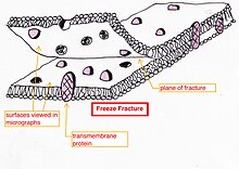
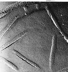
Freeze-fracture or freeze-etch – a preparation method particularly useful for examining lipid membranes and their incorporated proteins in "face on" view.Freeze-fracturing helps to peel open membranes to allow visualization of what is insideExternal
face of bakers yeast membrane showing the small holes where proteins
are fractured out, sometimes as small ring patterns.The fresh tissue or cell suspension is frozen rapidly (cryofixation), then fractured by breaking (or by using a microtome)
while maintained at liquid nitrogen temperature. The cold fractured
surface (sometimes "etched" by increasing the temperature to about
−100 °C for several minutes to let some ice sublime)
is then shadowed with evaporated platinum or gold at an average angle
of 45° in a high vacuum evaporator. The second coat of carbon,
evaporated perpendicular to the average surface plane is often performed
to improve the stability of the replica coating. The specimen is
returned to room temperature and pressure, then the extremely fragile
"pre-shadowed" metal replica of the fracture surface is released from
the underlying biological material by careful chemical digestion with
acids, hypochlorite solution or SDS
detergent. The still-floating replica is thoroughly washed free from
residual chemicals, carefully fished up on fine grids, dried then viewed
in the TEM.
Freeze-fracture replica immunogold labeling (FRIL) – the
freeze-fracture method has been modified to allow the identification of
the components of the fracture face by immunogold labeling. Instead of
removing all the underlying tissue of the thawed replica as the final
step before viewing in the microscope the tissue thickness is minimized
during or after the fracture process. The thin layer of tissue remains
bound to the metal replica so it can be immunogold labeled with
antibodies to the structures of choice. The thin layer of the original
specimen on the replica with gold attached allows the identification of
structures in the fracture plane. There are also related methods which label the surface of etched cells and other replica labeling variations.
Ion beam milling – thins samples until they are transparent to electrons by firing ions (typically argon) at the surface from an angle and sputtering material from the surface. A subclass of this is focused ion beam milling, where gallium
ions are used to produce an electron transparent membrane or 'lamella'
in a specific region of the sample, for example through a device within a
microprocessor or a focused ion beam
SEM. Ion beam milling may also be used for cross-section polishing
prior to analysis of materials that are difficult to prepare using
mechanical polishing.
Negative stain
– suspensions containing nanoparticles or fine biological material
(such as viruses and bacteria) are briefly mixed with a dilute solution
of an electron-opaque solution such as ammonium molybdate, uranyl
acetate (or formate), or phosphotungstic acid. This mixture is applied
to a suitably coated EM grid, blotted, then allowed to dry. Viewing of
this preparation in the TEM should be carried out without delay for best
results. The method is important in microbiology for fast but crude
morphological identification, but can also be used as the basis for
high-resolution 3D reconstruction using EM tomography methodology when
carbon films are used for support. Negative staining is also used for
observation of nanoparticles.
Sectioning – produces thin slices of the specimen, semitransparent to electrons. These can be cut using ultramicrotomy on an ultramicrotome with a glass or diamond knife to produce ultra-thin sections about 60–90 nm thick. Disposable glass knives are also used because they can be made in the lab and are much cheaper. Sections can also be created in situ by milling in a focused ion beam SEM, where the section is known as a lamella.
Staining – uses heavy metals such as lead, uranium or tungsten
to scatter imaging electrons and thus give contrast between different
structures, since many (especially biological) materials are nearly
"transparent" to electrons (weak phase objects). In biology, specimens
can be stained "en bloc" before embedding and also later after
sectioning. Typically thin sections are stained for several minutes with
an aqueous or alcoholic solution of uranyl acetate followed by aqueous lead citrate.
Disadvantages
JEOL transmission and scanning electron microscope made in the mid-1970s
Electron microscopes are expensive to build and maintain. Microscopes
designed to achieve high resolutions must be housed in stable buildings
(sometimes underground) with special services such as magnetic field
canceling systems.
The samples largely have to be viewed in vacuum, as the molecules that make up air would scatter the electrons. An exception is liquid-phase electron microscopy using either a closed liquid cell or an environmental chamber, for example, in the environmental scanning electron microscope, which allows hydrated samples to be viewed in a low-pressure (up to 20 Torr or 2.7 kPa) wet environment. Various techniques for in situ electron microscopy of gaseous samples have been developed.
Scanning electron microscopes operating in conventional
high-vacuum mode usually image conductive specimens; therefore
non-conductive materials require conductive coating (gold/palladium
alloy, carbon, osmium, etc.). The low-voltage mode of modern microscopes
makes possible the observation of non-conductive specimens without
coating. Non-conductive materials can be imaged also by a variable
pressure (or environmental) scanning electron microscope.
Small, stable specimens such as carbon nanotubes, diatom
frustules and small mineral crystals (asbestos fibres, for example)
require no special treatment before being examined in the electron
microscope. Samples of hydrated materials, including almost all
biological specimens, have to be prepared in various ways to stabilize
them, reduce their thickness (ultrathin sectioning) and increase their
electron optical contrast (staining). These processes may result in artifacts,
but these can usually be identified by comparing the results obtained
by using radically different specimen preparation methods. Since the
1980s, analysis of cryofixed, vitrified specimens has also become increasingly used by scientists, further confirming the validity of this technique.