Search This Blog

Thursday, January 16, 2020

Transistor count

From Wikipedia, the free encyclopedia
https://en.wikipedia.org/wiki/Transistor_count
 
Plot of MOS transistor counts for microprocessors against dates of in­tro­duction. The curve shows counts doubling every two years, per Moore's law.
 
The transistor count is the number of transistors on an integrated circuit (IC). It typically refers to the number of MOSFETs (metal-oxide-semiconductor field-effect transistors, or MOS transistors) on an IC chip, as all modern ICs use MOSFETs. It is the most common measure of IC complexity (although the majority of transistors in modern microprocessors are contained in the cache memories, which consist mostly of the same memory cell circuits replicated many times). The rate at which MOS transistor counts have increased generally follows Moore's law, which observed that the transistor count doubles approximately every two years.

As of 2019, the largest transistor count in a commercially available microprocessor is 39.54 billion MOSFETs, in AMD's Zen 2 based Epyc Rome, which is a 3D integrated circuit (with eight dies in a single package) fabricated using TSMC's 7 nm FinFET semiconductor manufacturing process. As of 2018, the highest transistor count in a graphics processing unit (GPU) is Nvidia's GV100 Volta with 21.1 billion MOSFETs, manufactured using TSMC's 12 nm FinFET process. As of 2019, the highest transistor count in any IC chip is Samsung's 1 TB eUFS (3D-stacked) V-NAND flash memory chip, with 2 trillion floating-gate MOSFETs (4 bits per transistor). As of 2019, the highest transistor count in a non-memory chip is a deep learning engine called the Wafer Scale Engine by Cerebras, using a special design to route around any non-functional core on the device; it has 1.2 trillion MOSFETs, manufactured using TSMC's 16 nm FinFET process.

In terms of computer systems that consist of numerous integrated circuits, the supercomputer with the highest transistor count as of 2016 is the Chinese-designed Sunway TaihuLight, which has for all CPUs/nodes (1012 for the 10 million cores and for RAM 1015 for the 1.3 million GB) combined "about 400 trillion transistors in the processing part of the hardware" and "the DRAM includes about 12 quadrillion transistors, and that’s about 97 percent of all the transistors." To compare, the smallest computer, as of 2018 dwarfed by a grain of sand, has on the order of 100,000 transistors, and the one, fully programmable, with the fewest transistors ever has 130 transistors or fewer.

In terms of the total number of transistors in existence, it has been estimated that a total of 13 sextillion (1.3 × 10²²) MOSFETs have been manufactured worldwide between 1960 and 2018, accounting for at least 99.9% of all transistors. This makes the MOSFET the most widely manufactured device in history.

Transistor count

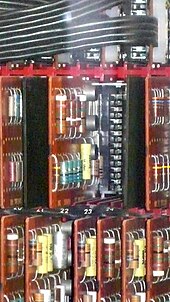
Part of an IBM 7070 card cage populated with Standard Modular System cards
 
Among the earliest products to use transistors were portable transistor radios, introduced in 1954, which typically used 4 to 8 transistors, often advertising the number on the radio's case. However, early junction transistors were relatively bulky devices that were difficult to manufacture on a mass-production basis, limiting the transistor counts and restricting their usage to a number of specialised applications.

The MOSFET (MOS transistor), invented by Mohamed Atalla and Dawon Kahng at Bell Labs in 1959, was the first truly compact transistor that could be miniaturised and mass-produced for a wide range of uses. The MOSFET made it possible to build high-density integrated circuits (ICs), enabling Moore's law and very large-scale integration. Atalla first proposed the concept of the MOS integrated circuit (MOS IC) chip in 1960, followed by Kahng in 1961, both noting that the MOSFET's ease of fabrication made it useful for integrated circuits. The earliest experimental MOS IC to be demonstrated was a 16-transistor chip built by Fred Heiman and Steven Hofstein at RCA Laboratories in 1962. Further large-scale integration was made possible with an improvement in MOSFET semiconductor device fabrication, the CMOS process, developed by Chih-Tang Sah and Frank Wanlass at Fairchild Semiconductor in 1963.

Microprocessors

A microprocessor incorporates the functions of a computer's central processing unit on a single integrated circuit. It is a multi-purpose, programmable device that accepts digital data as input, processes it according to instructions stored in its memory, and provides results as output.

The development of MOS integrated circuit technology in the 1960s led to the development of the first microprocessors. The 20-bit MP944, developed by Garrett AiResearch for the U.S. Navy's F-14 Tomcat fighter in 1970, is considered by its designer Ray Holt to be the first microprocessor. It was a multi-chip microprocessor, fabricated on six MOS chips. However, it was classified by the Navy until 1998. The 4-bit Intel 4004, released in 1971, was the first single-chip microprocessor. It was made possible with an improvement in MOSFET design, MOS silicon-gate technology (SGT), developed in 1968 at Fairchild Semiconductor by Federico Faggin, who went on to use MOS SGT technology to develop the 4004 with Marcian Hoff, Stanley Mazor and Masatoshi Shima at Intel.

All chips over e.g. a million transistors have lots of memory, usually cache memories in level 1 and 2 or more levels, accounting for most transistors on microprocessors in modern times, where large caches have become the norm. The level 1 caches of the Pentium Pro die accounted for over 14% of its transistors, while the much larger L2 cache was on a separate die, but on-package, so it's not included in the transistor count. Later chips included more levels, L2 or even L3 on-chip. The last DEC Alpha chip made has 90% of it for cache.

While Intel's i960CA small cache of 1 KB, at about 50,000 transistors, isn't a big part of the chip, it alone would have been very large in early microprocessors. In the ARM 3 chip, with 4 KB, the cache was over 63% of the chip, and in the Intel 80486 its larger cache is only over a third of it because the rest of the chip is more complex. So cache memories are the largest factor, except for in early chips with smaller caches or even earlier chips with no cache at all. Then the inherent complexity, e.g. number of instructions, is the dominant factor, more than e.g. the memory the registers of the chip represent.

GPUs

A graphics processing unit (GPU) is a specialized electronic circuit designed to rapidly manipulate and alter memory to accelerate the building of images in a frame buffer intended for output to a display. 

The designer refers to the technology company that designs the logic of the integrated circuit chip (such as Nvidia and AMD). The manufacturer refers to the semiconductor company that fabricates the chip using its semiconductor manufacturing process at a foundry (such as TSMC and Samsung Semiconductor). The transistor count in a chip is dependent on a manufacturer's fabrication process, with smaller semiconductor nodes typically enabling higher transistor density and thus higher transistor counts.

The random-access memory (RAM) that comes with GPUs (such as VRAM, SGRAM or HBM) greatly increase the total transistor count, with the memory typically accounting for the majority of transistors in a graphics card. For example, Nvidia's Tesla P100 has 15 billion FinFETs (16 nm) in the GPU in addition to 16 GB of HBM2 memory, totaling about 150 billion MOSFETs on the graphics card. 

Memory

Semiconductor memory is an electronic data storage device, often used as computer memory, implemented on integrated circuits. Nearly all semiconductor memory since the 1970s have used MOSFETs (MOS transistors), replacing earlier bipolar junction transistors. There are two major types of semiconductor memory, random-access memory (RAM) and non-volatile memory (NVM). In turn, there are two major RAM types, dynamic random-access memory (DRAM) and static random-access memory (SRAM), as well as two major NVM types, flash memory and read-only memory (ROM).

Typical CMOS SRAM consists of six transistors per cell. For DRAM, 1T1C, which means one transistor and one capacitor structure, is common. Capacitor charged or not is used to store 1 or 0. For flash memory, the data is stored in floating gate, and the resistance of the transistor is sensed to interpret the data stored. Depending on how fine scale the resistance could be separated, one transistor could store up to 3-bits, meaning eight distinctive level of resistance possible per transistor. However, the fine the scale comes with cost of repeatability therefore reliability. Typically, low grade 2-bits MLC flash is used for flash drives, so a 16 GB flash drive contains roughly 64 billion transistors.

For SRAM chips, six-transistor cells (six transistors per bit) was the standard. DRAM chips during the early 1970s had three-transistor cells (three transistors per bit), before single-transistor cells (one transistor per bit) became standard since the era of 4 Kb DRAM in the mid-1970s. In single-level flash memory, each cell contains one floating-gate MOSFET (one transistor per bit), whereas multi-level flash contains 2, 3 or 4 bits per transistor. 

Flash memory chips are commonly stacked up in layers, up to 128-layer in production, and 136-layer managed, and available in end-user devices up to 69-layer from manufacturers.

Transistor computers

Before transistors were invented, relays were used in early computers. The world's first working programmable, fully automatic digital computer, the 1941 Z3 22-bit word length computer, had 2,600 relays, and operated at a clock frequency of about 4–5 Hz. The 1940 Complex Number Computer had fewer than 500 relays, but it was not fully programmable. 

The second generation of computers were transistor computers that featured boards filled with discrete transistors and magnetic memory cores. The experimental 1953 48-bit Transistor Computer, developed at the University of Manchester, is widely believed to be the first transistor computer to come into operation anywhere in the world (the prototype had 92 point-contact transistors and 550 diodes). A later version the 1955 machine had a total of 250 junction transistors and 1300 point diodes. The Computer also used a small number of tubes in its clock generator, so it was not the first fully transistorized. The ETL Mark III, developed at the Electrotechnical Laboratory in 1956, may have been the first transistor-based electronic computer using the stored program method. It had about "130 point-contact transistors and about 1,800 germanium diodes were used for logic elements, and these were housed on 300 plug-in packages which could be slipped in and out. The 1958 decimal architecture IBM 7070 was the first transistor computer to be fully programmable. It had about 30,000 alloy-junction germanium transistors and 22,000 germanium diodes, on approximately 14,000 Standard Modular System (SMS) cards. The 1959 MOBIDIC, short for "MOBIle DIgital Computer", at 12,000 pounds (6.0 short tons) mounted in the trailer of a semi-trailer truck, was a transistorized computer for battlefield data. 

The third generation of computers used integrated circuits (ICs).[245] The 1962 15-bit Apollo Guidance Computer used "about 4,000 "Type-G" (3-input NOR gate) circuits" for about 12,000 transistors plus 32,000 resistors. The first commercial IC-based computer was the IBM System/360 in 1964. The 1965 12-bit PDP-8 CPU had 1409 transistors and over 10,000 diodes. It was not a microprocessor, as it used discrete transistors on many cards; but later microprocessors, such as the Intersil 6100 reimplemented it.

The next generation of computers were the microcomputers, also known as home computers or personal computers (PC), which used MOS microprocessors, in the 1970s. This list includes early transistorized computers (second generation) and IC-based computers (third generation) from the 1950s and 1960s. 

Parallel systems

Historically, each processing element in earlier parallel systems—like all CPUs of that time—was a serial computer built out of multiple chips. As transistor counts per chip increases, each processing element could be built out of fewer chips, and then later each multi-core processor chip could contain more processing elements.

Goodyear MPP: (1983?) 8 pixel processors per chip, 3,000 to 8,000 transistors per chip.

Brunel University Scape (single-chip array-processing element): (1983) 256 pixel processors per chip, 120,000 to 140,000 transistors per chip.

Cell Broadband Engine: (2006) with 9 cores per chip, had 234 million transistors per chip.

Transistor density

The transistor density is the number of transistors that are fabricated per unit area, typically measured in terms of the number of transistors per square millimeter (mm²). The transistor density usually correlates with the gate length of a semiconductor node (also known as a semiconductor manufacturing process), typically measured in nanometers (nm). As of 2019, the semiconductor node with the highest transistor density is TSMC's 5 nanometer node, with 171.3 million transistors per square millimeter.

Gallium nitride

From Wikipedia, the free encyclopedia
https://en.wikipedia.org/wiki/Gallium_nitride
 
Gallium nitride
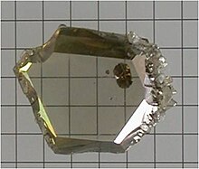
GaNcrystal.jpg
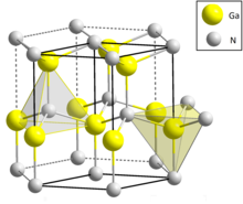
GaN Wurtzite polyhedra.png
Names
IUPAC name
Gallium nitride
Identifiers
3D model (JSmol)
ChemSpider
ECHA InfoCard 100.042.830
PubChem CID
Properties
GaN
Molar mass 83.730 g/mol
Appearance yellow powder
Density 6.1 g/cm3
Melting point >1600 °C
Insoluble
Band gap 3.4 eV (300 K, direct)
Electron mobility 1500 cm2/(V·s) (300 K)
Thermal conductivity 1.3 W/(cm·K) (300 K)
2.429
Structure
Wurtzite
C6v4-P63mc
a = 3.186 Å, c = 5.186 Å
Tetrahedral
Thermochemistry
−110.2 kJ/mol
Hazards
Flash point Non-flammable
Related compounds
Other anions
Gallium phosphide
Gallium arsenide
Gallium antimonide
Other cations
Boron nitride
Aluminium nitride
Indium nitride
Related compounds
Aluminium gallium arsenide
Indium gallium arsenide
Gallium arsenide phosphide
Aluminium gallium nitride
Indium gallium nitride
Except where otherwise noted, data are given for materials in their standard state (at 25 °C [77 °F], 100 kPa).
☑ verify (what is ☑☒ ?)
Infobox references

Gallium nitride (GaN) is a binary III/V direct bandgap semiconductor commonly used in light-emitting diodes since the 1990s. The compound is a very hard material that has a Wurtzite crystal structure. Its wide band gap of 3.4 eV affords it special properties for applications in optoelectronic, high-power and high-frequency devices. For example, GaN is the substrate which makes violet (405 nm) laser diodes possible, without use of nonlinear optical frequency-doubling.

Its sensitivity to ionizing radiation is low (like other group III nitrides), making it a suitable material for solar cell arrays for satellites. Military and space applications could also benefit as devices have shown stability in radiation environments.

Because GaN transistors can operate at much higher temperatures and work at much higher voltages than gallium arsenide (GaAs) transistors, they make ideal power amplifiers at microwave frequencies. In addition, GaN offers promising characteristics for THz devices.

Physical properties

GaN crystal

GaN is a very hard (12±2 GPa), mechanically stable wide bandgap semiconductor material with high heat capacity and thermal conductivity. In its pure form it resists cracking and can be deposited in thin film on sapphire or silicon carbide, despite the mismatch in their lattice constants. GaN can be doped with silicon (Si) or with oxygen to n-type and with magnesium (Mg) to p-type. However, the Si and Mg atoms change the way the GaN crystals grow, introducing tensile stresses and making them brittle. Gallium nitride compounds also tend to have a high dislocation density, on the order of 108 to 1010 defects per square centimeter. The wide band-gap behavior of GaN is connected to specific changes in the electronic band structure, charge occupation and chemical bond regions.

The U.S. Army Research Laboratory (ARL) provided the first measurement of the high field electron velocity in GaN in 1999. Scientists at ARL experimentally obtained a peak steady-state velocity of 1.9 x 107 cm/s, with a transit time of 2.5 picoseconds, attained at an electric field of 225 kV/cm. With this information, the electron mobility was calculated, thus providing data for the design of GaN devices. 

Developments

GaN with a high crystalline quality can be obtained by depositing a buffer layer at low temperatures. Such high-quality GaN led to the discovery of p-type GaN, p-n junction blue/UV-LEDs and room-temperature stimulated emission (essential for laser action). This has led to the commercialization of high-performance blue LEDs and long-lifetime violet-laser diodes, and to the development of nitride-based devices such as UV detectors and high-speed field-effect transistors.

LEDs

High-brightness GaN light-emitting diodes (LEDs) completed the range of primary colors, and made applications such as daylight visible full-color LED displays, white LEDs and blue laser devices possible. The first GaN-based high-brightness LEDs used a thin film of GaN deposited via Metal-Organic Vapour Phase Epitaxy (MOVPE) on sapphire. Other substrates used are zinc oxide, with lattice constant mismatch of only 2% and silicon carbide (SiC). Group III nitride semiconductors are, in general, recognized as one of the most promising semiconductor families for fabricating optical devices in the visible short-wavelength and UV region.

Transistors

The very high breakdown voltages, high electron mobility and saturation velocity of GaN has also made it an ideal candidate for high-power and high-temperature microwave applications, as evidenced by its high Johnson's figure of merit. Potential markets for high-power/high-frequency devices based on GaN include microwave radio-frequency power amplifiers (such as those used in high-speed wireless data transmission) and high-voltage switching devices for power grids. A potential mass-market application for GaN-based RF transistors is as the microwave source for microwave ovens, replacing the magnetrons currently used. The large band gap means that the performance of GaN transistors is maintained up to higher temperatures (~400 °C) than silicon transistors (~150 °C) because it lessens the effects of thermal generation of charge carriers that are inherent to any semiconductor. The first gallium nitride metal semiconductor field-effect transistors (GaN MESFET) were experimentally demonstrated in 1993 and they are being actively developed.

In 2010 the first enhancement-mode GaN transistors became generally available. Only n-channel transistors were available. These devices were designed to replace power MOSFETs in applications where switching speed or power conversion efficiency is critical. These transistors, also called eGaN FETs, are built by growing a thin layer of GaN on top of a standard silicon wafer. This allows the eGaN FETs to maintain costs similar to silicon power MOSFETs but with the superior electrical performance of GaN. 

Applications


LEDs

GaN-based violet laser diodes are used to read Blu-ray Discs. The mixture of GaN with In (InGaN) or Al (AlGaN) with a band gap dependent on ratio of In or Al to GaN allows the manufacture of light-emitting diodes (LEDs) with colors that can go from red to ultra-violet.

Transistors

GaN transistors are suitable for high frequency, high voltage, high temperature and high efficiency applications. 

GaN HEMTs have been offered commercially since 2006, and have found immediate use in various wireless infrastructure applications due to their high efficiency and high voltage operation. A second generation of devices with shorter gate lengths will address higher frequency telecom and aerospace applications.

GaN based MOSFET and MESFET transistors also offer advantages including lower loss in high power electronics, especially in automotive and electric car applications. Since 2008 these can be formed on a silicon substrate. High-voltage (800 V) Schottky barrier diodes (SBDs) have also been made.

GaN-based electronics (not pure GaN) has the potential to drastically cut energy consumption, not only in consumer applications but even for power transmission utilities.

Unlike silicon transistors which switch off due to power surges, GaN transistors are typically depletion mode devices (i.e. on / resistive when the gate-source voltage is zero). Several methods have been proposed to reach normally-off (or E-mode) operation, which is necessary for use in power electronics:
  • the implantation of fluorine ions under the gate (the negative charge of the F-ions favors the depletion of the channel)
  • the use of a MIS-type gate stack, with recess of the AlGaN
  • the integration of a cascaded pair constituted by a normally-on GaN transistor and a low voltage silicon MOSFET
  • the use of a p-type layer on top of the AlGaN/GaN heterojunction

Radars

They are also utilized in military electronics such as active electronically scanned array radars.

The U.S. Army funded Lockheed Martin to incorporate GaN active-device technology into the AN/TPQ-53 radar system to replace two medium-range radar systems, the AN/TPQ-36 and the AN/TPQ-37. The AN/TPQ-53 radar system was designed to detect, classify, track, and locate enemy indirect fire systems, as well as unmanned aerial systems. The AN/TPQ-53 radar system provided enhanced performance, greater mobility, increased reliability and supportability, lower life-cycle cost, and reduced crew size compared to the AN/TPQ-36 and the AN/TPQ-37 systems.

Lockheed Martin fielded other tactical operational radars with GaN technology in 2018, including TPS-77 Multi Role Radar System deployed to Latvia and Romania. In 2019, Lockheed Martin's partner ELTA Systems Limited, developed a GaN-based ELM-2084 Multi Mission Radar that was able to detect and track air craft and ballistic targets, while providing fire control guidance for missile interception or air defense artillery. 

Nanoscale

GaN nanotubes and nanowires are proposed for applications in nanoscale electronics, optoelectronics and biochemical-sensing applications.

Spintronics potential

When doped with a suitable transition metal such as manganese, GaN is a promising spintronics material (magnetic semiconductors).

Synthesis


Bulk substrates

GaN crystals can be grown from a molten Na/Ga melt held under 100 atmospheres of pressure of N2 at 750 °C. As Ga will not react with N2 below 1000 °C, the powder must be made from something more reactive, usually in one of the following ways:
2 Ga + 2 NH3 → 2 GaN + 3 H2
Ga2O3 + 2 NH3 → 2 GaN + 3 H2O
Gallium nitride can also be synthesized by injecting ammonia gas into molten gallium at 900-980 °C at normal atmospheric pressure.

Molecular beam epitaxy

Commercially, GaN crystals can be grown using molecular beam epitaxy or metalorganic vapour phase epitaxy. This process can be further modified to reduce dislocation densities. First, an ion beam is applied to the growth surface in order to create nanoscale roughness. Then, the surface is polished. This process takes place in a vacuum.

Safety

GaN dust is an irritant to skin, eyes and lungs. The environment, health and safety aspects of gallium nitride sources (such as trimethylgallium and ammonia) and industrial hygiene monitoring studies of MOVPE sources have been reported in a 2004 review.

Bulk GaN is non-toxic and biocompatible. Therefore, it may be used in the electrodes and electronics of implants in living organisms.

Epitaxy

From Wikipedia, the free encyclopedia

Crystallization
Process-of-Crystallization-200px.png
Concepts
Crystallization · Crystal growth
Recrystallization · Seed crystal
Protocrystalline · Single crystal
Methods and technology
Boules
Bridgman–Stockbarger technique
Crystal bar process
Czochralski process
Epitaxy Flux method
Fractional crystallization
Fractional freezing
Hydrothermal synthesis
Kyropoulos process
Laser-heated pedestal growth
Micro-pulling-down
Shaping processes in crystal growth
Skull crucible
Verneuil process
Zone melting
Fundamentals
Nucleation · Crystal
Crystal structure · Solid


The term epitaxy comes from the Greek roots epi (ἐπί), meaning "above", and taxis (τάξις), meaning "an ordered manner".

One of the main commercial applications of epitaxial growth is in the semiconductor industry, where semiconductor films are grown epitaxially on semiconductor substrate wafers. For the case of epitaxial growth of a planar film atop a substrate wafer, the epitaxial film's lattice will have a specific orientation relative to the substrate wafer's crystalline lattice such as the [001] Miller index of the film aligning with the [001] index of the substrate. In the simplest case, the epitaxial layer can be a continuation of the same exact semiconductor compound as the substrate; this is referred to as homoepitaxy. Otherwise, the epitaxial layer will be composed of a different compound; this is referred to as heteroepitaxy.

Types

Homoepitaxy is a kind of epitaxy performed with only one material, in which a crystalline film is grown on a substrate or film of the same material. This technology is used to grow a film which is more pure than the substrate and to fabricate layers having different doping levels. In academic literature, homoepitaxy is often abbreviated to "homoepi".

Homotopotaxy is a process similar to homoepitaxy except that the thin-film growth is not limited to two-dimensional growth. Here the substrate is the thin-film material.

Heteroepitaxy is a kind of epitaxy performed with materials that are different from each other. In heteroepitaxy, a crystalline film grows on a crystalline substrate or film of a different material. This technology is often used to grow crystalline films of materials for which crystals cannot otherwise be obtained and to fabricate integrated crystalline layers of different materials. Examples include silicon on sapphire, gallium nitride (GaN) on sapphire, aluminium gallium indium phosphide (AlGaInP) on gallium arsenide (GaAs) or diamond or iridium, and graphene on hexagonal boron nitride (hBN).

Heterotopotaxy is a process similar to heteroepitaxy except that thin-film growth is not limited to two-dimensional growth; the substrate is similar only in structure to the thin-film material.

Pendeo-epitaxy is a process in which the heteroepitaxial film is growing vertically and laterally at the same time. In 2D crystal heterostructure, graphene nanoribbons embedded in hexagonal boron nitride give an example of pendeo-epitaxy. 

Epitaxy is used in silicon-based manufacturing processes for bipolar junction transistors (BJTs) and modern complementary metal–oxide–semiconductors (CMOS), but it is particularly important for compound semiconductors such as gallium arsenide. Manufacturing issues include control of the amount and uniformity of the deposition's resistivity and thickness, the cleanliness and purity of the surface and the chamber atmosphere, the prevention of the typically much more highly doped substrate wafer's diffusion of dopant to the new layers, imperfections of the growth process, and protecting the surfaces during manufacture and handling. 

Applications

Epitaxy is used in nanotechnology and in semiconductor fabrication. Indeed, epitaxy is the only affordable method of high quality crystal growth for many semiconductor materials. In surface science, epitaxy is used to create and study monolayer and multilayer films of adsorbed organic molecules on single crystalline surfaces. Adsorbed molecules form ordered structures on atomically flat terraces of single crystalline surfaces and can directly be observed via scanning tunnelling microscopy. In contrast, surface defects and their geometry have significant influence on the adsorption of organic molecules.

Methods

Epitaxial silicon is usually grown using vapor-phase epitaxy (VPE), a modification of chemical vapor deposition. Molecular-beam and liquid-phase epitaxy (MBE and LPE) are also used, mainly for compound semiconductors. Solid-phase epitaxy is used primarily for crystal-damage healing.

Vapor-phase

Silicon is most commonly deposited by doping with silicon tetrachloride and hydrogen at approximately 1200 to 1250 °C:
SiCl4(g) + 2H2(g) ↔ Si(s) + 4HCl(g)
This reaction is reversible, and the growth rate depends strongly upon the proportion of the two source gases. Growth rates above 2 micrometres per minute produce polycrystalline silicon, and negative growth rates (etching) may occur if too much hydrogen chloride byproduct is present. (In fact, hydrogen chloride may be added intentionally to etch the wafer.) An additional etching reaction competes with the deposition reaction:
SiCl4(g) + Si(s) ↔ 2SiCl2(g)
Silicon VPE may also use silane, dichlorosilane, and trichlorosilane source gases. For instance, the silane reaction occurs at 650 °C in this way:
SiH4 → Si + 2H2
This reaction does not inadvertently etch the wafer, and takes place at lower temperatures than deposition from silicon tetrachloride. However, it will form a polycrystalline film unless tightly controlled, and it allows oxidizing species that leak into the reactor to contaminate the epitaxial layer with unwanted compounds such as silicon dioxide

VPE is sometimes classified by the chemistry of the source gases, such as hydride VPE and metalorganic VPE.

Liquid-phase

Liquid-phase epitaxy (LPE) is a method to grow semiconductor crystal layers from the melt on solid substrates. This happens at temperatures well below the melting point of the deposited semiconductor. The semiconductor is dissolved in the melt of another material. At conditions that are close to the equilibrium between dissolution and deposition, the deposition of the semiconductor crystal on the substrate is relatively fast and uniform. The most used substrate is indium phosphide (InP). Other substrates like glass or ceramic can be applied for special applications. To facilitate nucleation, and to avoid tension in the grown layer the thermal expansion coefficient of substrate and grown layer should be similar. 

Centrifugal liquid-phase epitaxy is used commercially to make thin layers of silicon, germanium, and gallium arsenide. Centrifugally formed film growth is a process used to form thin layers of materials by using a centrifuge. The process has been used to create silicon for thin-film solar cells and far-infrared photodetectors. Temperature and centrifuge spin rate are used to control layer growth. Centrifugal LPE has the capability to create dopant concentration gradients while the solution is held at constant temperature.

Solid-phase

Solid-phase epitaxy (SPE) is a transition between the amorphous and crystalline phases of a material. It is usually done by first depositing a film of amorphous material on a crystalline substrate. The substrate is then heated to crystallize the film. The single crystal substrate serves as a template for crystal growth. The annealing step used to recrystallize or heal silicon layers amorphized during ion implantation is also considered one type of Solid Phase Epitaxy. The Impurity segregation and redistribution at the growing crystal-amorphous layer interface during this process is used to incorporate low-solubility dopants in metals and Silicon.

Molecular-beam epitaxy

In molecular beam epitaxy (MBE), a source material is heated to produce an evaporated beam of particles. These particles travel through a very high vacuum (10−8 Pa; practically free space) to the substrate, where they condense. MBE has lower throughput than other forms of epitaxy. This technique is widely used for growing periodic groups III, IV, and V semiconductor crystals.

Doping

An epitaxial layer can be doped during deposition by adding impurities to the source gas, such as arsine, phosphine, or diborane. The concentration of impurity in the gas phase determines its concentration in the deposited film. As in chemical vapor deposition (CVD), impurities change the deposition rate. Additionally, the high temperatures at which CVD is performed may allow dopants to diffuse into the growing layer from other layers in the wafer ("out-diffusion"). Also, dopants in the source gas, liberated by evaporation or wet etching of the surface, may diffuse into the epitaxial layer ("autodoping"). The dopant profiles of underlying layers change as well, however not as significantly.

Minerals

text
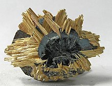
Rutile epitaxial on hematite nearly 6 cm long. Bahia, Brazil

In mineralogy, epitaxy is the overgrowth of one mineral on another in an orderly way, such that certain crystal directions of the two minerals are aligned. This occurs when some planes in the lattices of the overgrowth and the substrate have similar spacings between atoms.

If the crystals of both minerals are well formed so that the directions of the crystallographic axes are clear then the epitaxic relationship can be deduced just by a visual inspection.

Sometimes many separate crystals form the overgrowth on a single substrate, and then if there is epitaxy all the overgrowth crystals will have a similar orientation. The reverse, however, is not necessarily true. If the overgrowth crystals have a similar orientation there is probably an epitaxic relationship, but it is not certain.

Some authors consider that overgrowths of a second generation of the same mineral species should also be considered as epitaxy, and this is common terminology for semiconductor scientists who induce epitaxic growth of a film with a different doping level on a semiconductor substrate of the same material. For naturally produced minerals, however, the International Mineralogical Association (IMA) definition requires that the two minerals be of different species.

Another man-made application of epitaxy is the making of artificial snow using silver iodide, which is possible because hexagonal silver iodide and ice have similar cell dimensions.

Isomorphic minerals

Minerals that have the same structure (isomorphic minerals) may have epitaxic relations. An example is albite NaAlSi
3
O
8
on microcline KAlSi
3
O
8
. Both these minerals are triclinic, with space group 1, and with similar unit cell parameters, a = 8.16 Å, b = 12.87 Å, c = 7.11 Å, α = 93.45°, β = 116.4°, γ = 90.28° for albite and a = 8.5784 Å, b = 12.96 Å, c = 7.2112 Å, α = 90.3°, β = 116.05°, γ = 89° for microcline. 

Polymorphic minerals

text
Rutile on hematite, from Novo Horizonte, Bahia, Northeast Region, Brazil
text
Hematite pseudomorph after magnetite, with terraced epitaxial faces. La Rioja, Argentina
Minerals that have the same composition but different structures (polymorphic minerals) may also have epitaxic relations. Examples are pyrite and marcasite, both FeS2, and sphalerite and wurtzite, both ZnS.

Rutile on hematite

Some pairs of minerals that are not related structurally or compositionally may also exhibit epitaxy. A common example is rutile TiO2 on hematite Template:Fe. Rutile is tetragonal and hematite is trigonal, but there are directions of similar spacing between the atoms in the (100) plane of rutile (perpendicular to the a axis) and the (001) plane of hematite (perpendicular to the c axis). In epitaxy these directions tend to line up with each other, resulting in the axis of the rutile overgrowth being parallel to the c axis of hematite, and the c axis of rutile being parallel to one of the axes of hematite.

Hematite on magnetite

Another example is hematite Fe3+
2
O
3
on magnetite Fe2+Fe3+
2
O
4
. The magnetite structure is based on close-packed oxygen anions stacked in an ABC-ABC sequence. In this packing the close-packed layers are parallel to (111) (a plane that symmetrically "cuts off" a corner of a cube). The hematite structure is based on close-packed oxygen anions stacked in an AB-AB sequence, which results in a crystal with hexagonal symmetry.

If the cations were small enough to fit into a truly close-packed structure of oxygen anions then the spacing between the nearest neighbour oxygen sites would be the same for both species. The radius of the oxygen ion, however, is only 1.36 Å and the Fe cations are big enough to cause some variations. The Fe radii vary from 0.49 Å to 0.92 Å, depending on the charge (2+ or 3+) and the coordination number (4 or 8). Nevertheless, the O spacings are similar for the two minerals hence hematite can readily grow on the (111) faces of magnetite, with hematite (001) parallel to magnetite (111).

Equality (mathematics)

From Wikipedia, the free encyclopedia https://en.wikipedia.org/wiki/Equality_...