Search This Blog

Wednesday, May 22, 2024

Software development

From Wikipedia, the free encyclopedia
(Redirected from Collaborative software development model)

Software development
is the process used to create software. Programming and maintaining the source code is the central step of this process, but it also includes conceiving the project, evaluating its feasibility, analyzing the business requirements, software design, testing, to release. Software engineering, in addition to development, also includes project management, employee management, and other overhead functions. Software development may be sequential, in which each step is complete before the next begins, but iterative development methods where multiple steps can be executed at once and earlier steps can be revisited have also been devised to improve flexibility, efficiency, and scheduling.

Software development involves professionals from various fields, not just software programmers but also individuals specialized in testing, documentation writing, graphic design, user support, marketing, and fundraising. A number of tools and models are commonly used in software development, such as integrated development environment (IDE), version control, computer-aided software engineering, and software documentation.

Methodologies

Flowchart of the evolutionary prototyping model, an iterative development model

Each of the available methodologies are best suited to specific kinds of projects, based on various technical, organizational, project, and team considerations.

  • The simplest methodology is the "code and fix", typically used by a single programmer working on a small project. After briefly considering the purpose of the program, the programmer codes it and runs it to see if it works. When they are done, the product is released. This methodology is useful for prototypes but cannot be used for more elaborate programs.
  • In the top-down waterfall model, feasibility, analysis, design, development, quality assurance, and implementation occur sequentially in that order. This model requires one step to be complete before the next begins, causing delays, and makes it impossible to revise previous steps if necessary.
  • With iterative processes these steps are interleaved with each other for improved flexibility, efficiency, and more realistic scheduling. Instead of completing the project all at once, one might go through most of the steps with one component at a time. Iterative development also lets developers prioritize the most important features, enabling lower priority ones to be dropped later on if necessary. Agile is one popular method, originally intended for small or medium sized projects, that focuses on giving developers more control over the features that they work on to reduce the risk of time or cost overruns. Derivatives of agile include extreme programming and Scrum. Open-source software development typically uses agile methodology with concurrent design, coding, and testing, due to reliance on a distributed network of volunteer contributors.
  • Beyond agile, some companies integrate information technology (IT) operations with software development, which is called DevOps or DevSecOps including computer security. DevOps includes continuous development, testing, integration of new code in the version control system, deployment of the new code, and sometimes delivery of the code to clients. The purpose of this integration is to deliver IT services more quickly and efficiently.

Another focus in many programming methodologies is the idea of trying to catch issues such as security vulnerabilities and bugs as early as possible (shift-left testing) to reduce the cost of tracking and fixing them.

In 2009, it was estimated that 32 percent of software projects were delivered on time and budget, and with the full functionality. An additional 44 percent were delivered, but missing at least one of these features. The remaining 24 percent were cancelled prior to release.

Steps

Software development life cycle refers to the systematic process of developing applications.

Feasibility

The sources of ideas for software products are plentiful. These ideas can come from market research including the demographics of potential new customers, existing customers, sales prospects who rejected the product, other internal software development staff, or a creative third party. Ideas for software products are usually first evaluated by marketing personnel for economic feasibility, fit with existing channels of distribution, possible effects on existing product lines, required features, and fit with the company's marketing objectives. In the marketing evaluation phase, the cost and time assumptions become evaluated. The feasibility analysis estimates the project's return on investment, its development cost and timeframe. Based on this analysis, the company can make a business decision to invest in further development. After deciding to develop the software, the company is focused on delivering the product at or below the estimated cost and time, and with a high standard of quality (i.e., lack of bugs) and the desired functionality. Nevertheless, most software projects run late and sometimes compromises are made in features or quality to meet a deadline.

Analysis

Software analysis begins with a requirements analysis to capture the business needs of the software. Challenges for the identification of needs are that current or potential users may have different and incompatible needs, may not understand their own needs, and change their needs during the process of software development. Ultimately, the result of analysis is a detailed specification for the product that developers can work from. Software analysts often decompose the project into smaller objects, components that can be reused for increased cost-effectiveness, efficiency, and reliability. Decomposing the project may enable a multi-threaded implementation that runs significantly faster on multiprocessor computers.

During the analysis and design phases of software development, structured analysis is often used to break down the customer's requirements into pieces that can be implemented by software programmers. The underlying logic of the program may be represented in data-flow diagrams, data dictionaries, pseudocode, state transition diagrams, and/or entity relationship diagrams. If the project incorporates a piece of legacy software that has not been modeled, this software may be modeled to help ensure it is correctly incorporated with the newer software.

Design

Design involves choices about the implementation of the software, such as which programming languages and database software to use, or how the hardware and network communications will be organized. Design may be iterative with users consulted about their needs in a process of trial and error. Design often involves people expert in aspect such as database design, screen architecture, and the performance of servers and other hardware. Designers often attempt to find patterns in the software's functionality to spin off distinct modules that can be reused with object-oriented programming. An example of this is the model–view–controller, an interface between a graphical user interface and the backend.

Programming

The central feature of software development is creating and understanding the software that implements the desired functionality. There are various strategies for writing the code. Cohesive software has various components that are independent from each other. Coupling is the interrelation of different software components, which is viewed as undesirable because it increases the difficulty of maintenance. Often, software programmers do not follow industry best practices, resulting in code that is inefficient, difficult to understand, or lacking documentation on its functionality. These standards are especially likely to break down in the presence of deadlines. As a result, testing, debugging, and revising the code becomes much more difficult. Code refactoring, for example adding more comments to the code, is a solution to improve the understandibility of code.

Testing

Testing is the process of ensuring that the code executes correctly and without errors. Debugging is performed by each software developer on their own code to confirm that the code does what it is intended to. In particular, it is crucial that the software executes on all inputs, even if the result is incorrect. Code reviews by other developers are often used to scrutinize new code added to the project, and according to some estimates dramatically reduce the number of bugs persisting after testing is complete. Once the code has been submitted, quality assurance—a separate department of non-programmers for most large companies—test the accuracy of the entire software product. Acceptance tests derived from the original software requirements are a popular tool for this. Quality testing also often includes stress and load checking (whether the software is robust to heavy levels of input or usage), integration testing (to ensure that the software is adequately integrated with other software), and compatibility testing (measuring the software's performance across different operating systems or browsers). When tests are written before the code, this is called test-driven development.

Production

Production is the phase in which software is deployed to the end user. During production, the developer may create technical support resources for users or a process for fixing bugs and errors that were not caught earlier. There might also be a return to earlier development phases if user needs changed or were misunderstood.

Workers

Software development is performed by software developers, usually working on a team. Efficient communications between team members is essential to success. This is more easily achieved if the team is small, used to working together, and located near each other. Communications also help identify problems at an earlier state of development and avoid duplicated effort. Many development projects avoid the risk of losing essential knowledge held by only one employee by ensuring that multiple workers are familiar with each component. Software development involves professionals from various fields, not just software programmers but also individuals specialized in testing, documentation writing, graphic design, user support, marketing, and fundraising. Although workers for proprietary software are paid, most contributors to open-source software are volunteers. Alternately, they may be paid by companies whose business model does not involve selling the software, but something else—such as services and modifications to open source software.

Models and tools

Computer-aided software engineering

Computer-aided software engineering (CASE) is tools for the partial automation of software development. CASE enables designers to sketch out the logic of a program, whether one to be written, or an already existing one to help integrate it with new code or reverse engineer it (for example, to change the programming language).

Documentation

Documentation comes in two forms that are usually kept separate—that intended for software developers, and that made available to the end user to help them use the software. Most developer documentation is in the form of code comments for each file, class, and method that cover the application programming interface (API)—how the piece of software can be accessed by another—and often implementation details. This documentation is helpful for new developers to understand the project when they begin working on it. In agile development, the documentation is often written at the same time as the code. User documentation is more frequently written by technical writers.

Effort estimation

Accurate estimation is crucial at the feasibility stage and in delivering the product on time and within budget. The process of generating estimations is often delegated by the project manager. Because the effort estimation is directly related to the size of the complete application, it is strongly influenced by addition of features in the requirements—the more requirements, the higher the development cost. Aspects not related to functionality, such as the experience of the software developers and code reusability, are also essential to consider in estimation. As of 2019, most of the tools for estimating the amount of time and resources for software development were designed for conventional applications and are not applicable to web applications or mobile applications.

Integrated development environment
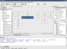
Anjuta, a C and C++ IDE for the GNOME environment

An integrated development environment (IDE) supports software development with enhanced features compared to a simple text editor. IDEs often include automated compiling, syntax highlighting of errors, debugging assistance, integration with version control, and semi-automation of tests.

Version control

Version control is a popular way of managing changes made to the software. Whenever a new version is checked in, the software saves a backup of all modified files. If multiple programmers are working on the software simultaneously, it manages the merging of their code changes. The software highlights cases where there is a conflict between two sets of changes and allows programmers to fix the conflict.

View model

The TEAF Matrix of Views and Perspectives

A view model is a framework that provides the viewpoints on the system and its environment, to be used in the software development process. It is a graphical representation of the underlying semantics of a view.

The purpose of viewpoints and views is to enable human engineers to comprehend very complex systems and to organize the elements of the problem around domains of expertise. In the engineering of physically intensive systems, viewpoints often correspond to capabilities and responsibilities within the engineering organization.

Intellectual property

Intellectual property can be an issue when developers integrate open-source code or libraries into a proprietary product, because most open-source licenses used for software require that modifications be released under the same license. As an alternative, developers may choose a proprietary alternative or write their own software module.

Smart manufacturing

From Wikipedia, the free encyclopedia
Smart manufacturing is a broad category of manufacturing that employs computer-integrated manufacturing, high levels of adaptability and rapid design changes, digital information technology, and more flexible technical workforce training. Other goals sometimes include fast changes in production levels based on demand, optimization of the supply chain, efficient production and recyclability. In this concept, as smart factory has interoperable systems, multi-scale dynamic modelling and simulation, intelligent automation, strong cyber security, and networked sensors.

The broad definition of smart manufacturing covers many different technologies. Some of the key technologies in the smart manufacturing movement include big data processing capabilities, industrial connectivity devices and services, and advanced robotics.

Graphic of a sample manufacturing control system showing the interconnectivity of data analysis, computing and automation. Graphic of a sample manufacturing control system showing the interconnectivity of data analysis, computing and automation
Advanced robotics used in automotive production

Big data processing

Smart manufacturing utilizes big data analytics, to refine complicated processes and manage supply chains. Big data analytics refers to a method for gathering and understanding large data sets in terms of what are known as the three V's, velocity, variety and volume. Velocity informs the frequency of data acquisition, which can be concurrent with the application of previous data. Variety describes the different types of data that may be handled. Volume represents the amount of data. Big data analytics allows an enterprise to use smart manufacturing to predict demand and the need for design changes rather than reacting to orders placed.

Some products have embedded sensors, which produce large amounts of data that can be used to understand consumer behavior and improve future versions of the product.

Advanced robotics

Advanced industrial robots, also known as smart machines, operate autonomously and can communicate directly with manufacturing systems. In some advanced manufacturing contexts, they can work with humans for co-assembly tasks. By evaluating sensory input and distinguishing between different product configurations, these machines are able to solve problems and make decisions independent of people. These robots are able to complete work beyond what they were initially programmed to do and have artificial intelligence that allows them to learn from experience. These machines have the flexibility to be reconfigured and re-purposed. This gives them the ability to respond rapidly to design changes and innovation, which is a competitive advantage over more traditional manufacturing processes. An area of concern surrounding advanced robotics is the safety and well-being of the human workers who interact with robotic systems. Traditionally, measures have been taken to segregate robots from the human workforce, but advances in robotic cognitive ability have opened up opportunities, such as cobots, for robots to work collaboratively with people.

Cloud computing allows large amounts of data storage or computational power to be rapidly applied to manufacturing, and allow a large amount of data on machine performance and output quality to be collected. This can improve machine configuration, predictive maintenance, and fault analysis. Better predictions can facilitate better strategies for ordering raw materials or scheduling production runs.

3D printing

As of 2019, 3D printing is mainly used in rapid prototyping, design iteration, and small-scale production. Improvements in speed, quality, and materials could make it useful in mass production and mass customization.

However, 3D printing developed so much in recent years that it is no longer used just as technology for prototyping. 3D printing sector is moving beyond prototyping especially it is becoming increasingly widespread in supply chains. The industries where digital manufacturing with 3D printing is the most seen are automotive, industrial and medical. In the auto industry, 3D printing is used not only for prototyping but also for the full production of final parts and products. 3D printing has also been used by suppliers and digital manufacturers coming together to help fight COVID-19.

3D printing allows to prototype more successfully, thus companies are saving time and money as significant volumes of parts can be produced in a short period. There is great potential for 3D printing to revolutionise supply chains, hence more companies are using it. The main challenge that 3D printing faces is the change of people's mindset. Moreover, some workers will need to re-learn a set of new skills to manage 3D printing technology.

Eliminating workplace inefficiencies and hazards

Smart manufacturing can also be attributed to surveying workplace inefficiencies and assisting in worker safety. Efficiency optimization is a huge focus for adopters of "smart" systems, which is done through data research and intelligent learning automation. For instance operators can be given personal access cards with inbuilt Wi-Fi and Bluetooth, which can connect to the machines and a Cloud platform to determine which operator is working on which machine in real time. An intelligent, interconnected 'smart' system can be established to set a performance target, determine if the target is obtainable, and identify inefficiencies through failed or delayed performance targets. In general, automation may alleviate inefficiencies due to human error. And in general, evolving AI eliminates the inefficiencies of its predecessors.

As robots take on more of the physical tasks of manufacturing, workers no longer need to be present and are exposed to fewer hazards.

Impact of Industry 4.0

Industry 4.0 is a project in the high-tech strategy of the German government that promotes the computerization of traditional industries such as manufacturing. The goal is the intelligent factory (Smart Factory) that is characterized by adaptability, resource efficiency, and ergonomics, as well as the integration of customers and business partners in business and value processes. Its technological foundation consists of cyber-physical systems and the Internet of Things.

This kind of "intelligent manufacturing" makes a great use of:

  • Wireless connections, both during product assembly and long-distance interactions with them;
  • Last generation sensors, distributed along the supply chain and the same products (Internet of things)
  • Elaboration of a great amount of data to control all phases of construction, distribution and usage of a good.

European Roadmap "Factories of the Future" and German one "Industrie 4.0″ illustrate several of the action lines to undertake and the related benefits. Some examples are:

  • Advanced manufacturing processes and rapid prototyping will make possible for each customer to order one-of-a-kind product without significant cost increase.
  • Collaborative Virtual Factory (VF) platforms will drastically reduce cost and time associated to new product design and engineering of the production process, by exploiting complete simulation and virtual testing throughout the Product Lifecycle.
  • Advanced Human-Machine interaction (HMI) and augmented reality (AR) devices will help increasing safety in production plants and reducing physical demand to workers (whose age has an increasing trend).
  • Machine learning will be fundamental to optimize the production processes, both for reducing lead times and reducing the energy consumption.
  • Cyber-physical systems and machine-to-machine (M2M) communication will allow to gather and share real-time data from the shop floor in order to reduce downtime and idle time by conducting extremely effective predictive maintenance.

Statistics

The Ministry of Economy, Trade and Industry in South Korea announced on 10 March 2016 that it had aided the construction of smart factories in 1,240 small and medium enterprises, which it said resulted in an average 27.6% decrease in defective products, 7.1% faster production of prototypes, and 29.2% lower cost.

Tuesday, May 21, 2024

Electronic design automation

From Wikipedia, the free encyclopedia
https://en.wikipedia.org/wiki/Electronic_design_automation

Electronic design automation (EDA), also referred to as electronic computer-aided design (ECAD), is a category of software tools for designing electronic systems such as integrated circuits and printed circuit boards. The tools work together in a design flow that chip designers use to design and analyze entire semiconductor chips. Since a modern semiconductor chip can have billions of components, EDA tools are essential for their design; this article in particular describes EDA specifically with respect to integrated circuits (ICs).

History

Early days

The earliest electronic design automation is attributed to IBM with the documentation of its 700 series computers in the 1950s.

Prior to the development of EDA, integrated circuits were designed by hand and manually laid out. Some advanced shops used geometric software to generate tapes for a Gerber photoplotter, responsible for generating a monochromatic exposure image, but even those copied digital recordings of mechanically drawn components. The process was fundamentally graphic, with the translation from electronics to graphics done manually; the best-known company from this era was Calma, whose GDSII format is still in use today. By the mid-1970s, developers started to automate circuit design in addition to drafting and the first placement and routing tools were developed; as this occurred, the proceedings of the Design Automation Conference catalogued the large majority of the developments of the time.

The next era began following the publication of "Introduction to VLSI Systems" by Carver Mead and Lynn Conway in 1980; considered the standard textbook for chip design. The result was an increase in the complexity of the chips that could be designed, with improved access to design verification tools that used logic simulation. The chips were easier to lay out and more likely to function correctly, since their designs could be simulated more thoroughly prior to construction. Although the languages and tools have evolved, this general approach of specifying the desired behavior in a textual programming language and letting the tools derive the detailed physical design remains the basis of digital IC design today.

The earliest EDA tools were produced academically. One of the most famous was the "Berkeley VLSI Tools Tarball", a set of UNIX utilities used to design early VLSI systems. Widely used were the Espresso heuristic logic minimizer, responsible for circuit complexity reductions and Magic, a computer-aided design platform. Another crucial development was the formation of MOSIS, a consortium of universities and fabricators that developed an inexpensive way to train student chip designers by producing real integrated circuits. The basic concept was to use reliable, low-cost, relatively low-technology IC processes and pack a large number of projects per wafer, with several copies of chips from each project remaining preserved. Cooperating fabricators either donated the processed wafers or sold them at cost, as they saw the program as helpful to their own long-term growth.

Commercial birth

1981 marked the beginning of EDA as an industry. For many years, the larger electronic companies, such as Hewlett-Packard, Tektronix and Intel, had pursued EDA internally, with managers and developers beginning to spin out of these companies to concentrate on EDA as a business. Daisy Systems, Mentor Graphics and Valid Logic Systems were all founded around this time and collectively referred to as DMV. In 1981, the U.S. Department of Defense additionally began funding of VHDL as a hardware description language. Within a few years, there were many companies specializing in EDA, each with a slightly different emphasis.

The first trade show for EDA was held at the Design Automation Conference in 1984 and in 1986, Verilog, another popular high-level design language, was first introduced as a hardware description language by Gateway Design Automation. Simulators quickly followed these introductions, permitting direct simulation of chip designs and executable specifications. Within several years, back-ends were developed to perform logic synthesis.

Modern day

Current digital flows are extremely modular, with front ends producing standardized design descriptions that compile into invocations of units similar to cells without regard to their individual technology. Cells implement logic or other electronic functions via the utilisation of a particular integrated circuit technology. Fabricators generally provide libraries of components for their production processes, with simulation models that fit standard simulation tools.

Most analog circuits are still designed in a manual fashion, requiring specialist knowledge that is unique to analog design (such as matching concepts). Hence, analog EDA tools are far less modular, since many more functions are required, they interact more strongly and the components are, in general, less ideal.

EDA for electronics has rapidly increased in importance with the continuous scaling of semiconductor technology. Some users are foundry operators, who operate the semiconductor fabrication facilities ("fabs") and additional individuals responsible for utilising the technology design-service companies who use EDA software to evaluate an incoming design for manufacturing readiness. EDA tools are also used for programming design functionality into FPGAs or field-programmable gate arrays, customisable integrated circuit designs.

Software focuses

Design

Design flow primarily remains characterised via several primary components; these include:

  • High-level synthesis (additionally known as behavioral synthesis or algorithmic synthesis) – The high-level design description (e.g. in C/C++) is converted into RTL or the register transfer level, responsible for representing circuitry via the utilisation of interactions between registers.
  • Logic synthesis – The translation of RTL design description (e.g. written in Verilog or VHDL) into a discrete netlist or representation of logic gates.
  • Schematic capture – For standard cell digital, analog, RF-like Capture CIS in Orcad by Cadence and ISIS in Proteus.
  • Layout – usually schematic-driven layout, like Layout in Orcad by Cadence, ARES in Proteus

Simulation

  • Transistor simulation – low-level transistor-simulation of a schematic/layout's behavior, accurate at device-level.
  • Logic simulation – digital-simulation of an RTL or gate-netlist's digital (Boolean 0/1) behavior, accurate at Boolean-level.
  • Behavioral simulation – high-level simulation of a design's architectural operation, accurate at cycle-level or interface-level.
  • Hardware emulation – Use of special purpose hardware to emulate the logic of a proposed design. Can sometimes be plugged into a system in place of a yet-to-be-built chip; this is called in-circuit emulation.
  • Technology CAD simulate and analyze the underlying process technology. Electrical properties of devices are derived directly from device physics
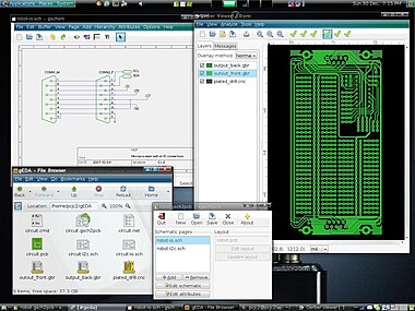
Schematic capture program

Analysis and verification

  • Functional verification: ensures logic design matches specifications and executes tasks correctly. Includes dynamic functional verification via simulation, emulation, and prototypes.
  • RTL Linting for adherence to coding rules such as syntax, semantics, and style.
  • Clock domain crossing verification (CDC check): similar to linting, but these checks/tools specialize in detecting and reporting potential issues like data loss, meta-stability due to use of multiple clock domains in the design.
  • Formal verification, also model checking: attempts to prove, by mathematical methods, that the system has certain desired properties, and that some undesired effects (such as deadlock) cannot occur.
  • Equivalence checking: algorithmic comparison between a chip's RTL-description and synthesized gate-netlist, to ensure functional equivalence at the logical level.
  • Static timing analysis: analysis of the timing of a circuit in an input-independent manner, hence finding a worst case over all possible inputs.
  • Layout extraction: starting with a proposed layout, compute the (approximate) electrical characteristics of every wire and device. Often used in conjunction with static timing analysis above to estimate the performance of the completed chip.
  • Electromagnetic field solvers, or just field solvers, solve Maxwell's equations directly for cases of interest in IC and PCB design. They are known for being slower but more accurate than the layout extraction above.
  • Physical verification, PV: checking if a design is physically manufacturable, and that the resulting chips will not have any function-preventing physical defects, and will meet original specifications.

Manufacturing preparation

Functional safety

  • Functional safety analysis, systematic computation of failure in time (FIT) rates and diagnostic coverage metrics for designs in order to meet the compliance requirements for the desired safety integrity levels.
  • Functional safety synthesis, add reliability enhancements to structured elements (modules, RAMs, ROMs, register files, FIFOs) to improve fault detection / fault tolerance. This includes (not limited to) addition of error detection and / or correction codes (Hamming), redundant logic for fault detection and fault tolerance (duplicate / triplicate) and protocol checks (interface parity, address alignment, beat count)
  • Functional safety verification, running of a fault campaign, including insertion of faults into the design and verification that the safety mechanism reacts in an appropriate manner for the faults that are deemed covered.
PCB layout and schematic for connector design

Companies

Current

Market capitalization and company name as of March 2023:

Defunct

Market capitalization and company name as of December 2011:

Acquisitions

Many EDA companies acquire small companies with software or other technology that can be adapted to their core business. Most of the market leaders are amalgamations of many smaller companies and this trend is helped by the tendency of software companies to design tools as accessories that fit naturally into a larger vendor's suite of programs on digital circuitry; many new tools incorporate analog design and mixed systems. This is happening due to a trend to place entire electronic systems on a single chip.

Technical conferences

Scanning probe microscopy

From Wikipedia, the free encyclopedia
https://en.wikipedia.org/wiki/Scanning_probe_microscopy

Scanning probe microscopy (SPM) is a branch of microscopy that forms images of surfaces using a physical probe that scans the specimen. SPM was founded in 1981, with the invention of the scanning tunneling microscope, an instrument for imaging surfaces at the atomic level. The first successful scanning tunneling microscope experiment was done by Gerd Binnig and Heinrich Rohrer. The key to their success was using a feedback loop to regulate gap distance between the sample and the probe.

Many scanning probe microscopes can image several interactions simultaneously. The manner of using these interactions to obtain an image is generally called a mode.

The resolution varies somewhat from technique to technique, but some probe techniques reach a rather impressive atomic resolution. This is due largely because piezoelectric actuators can execute motions with a precision and accuracy at the atomic level or better on electronic command. This family of techniques can be called "piezoelectric techniques". The other common denominator is that the data are typically obtained as a two-dimensional grid of data points, visualized in false color as a computer image.

Established types

Image formation

To form images, scanning probe microscopes raster scan the tip over the surface. At discrete points in the raster scan a value is recorded (which value depends on the type of SPM and the mode of operation, see below). These recorded values are displayed as a heat map to produce the final STM images, usually using a black and white or an orange color scale.

Constant interaction mode

In constant interaction mode (often referred to as "in feedback"), a feedback loop is used to physically move the probe closer to or further from the surface (in the z axis) under study to maintain a constant interaction. This interaction depends on the type of SPM, for scanning tunneling microscopy the interaction is the tunnel current, for contact mode AFM or MFM it is the cantilever deflection, etc. The type of feedback loop used is usually a PI-loop, which is a PID-loop where the differential gain has been set to zero (as it amplifies noise). The z position of the tip (scanning plane is the xy-plane) is recorded periodically and displayed as a heat map. This is normally referred to as a topography image.

In this mode a second image, known as the ″error signal" or "error image" is also taken, which is a heat map of the interaction which was fed back on. Under perfect operation this image would be a blank at a constant value which was set on the feedback loop. Under real operation the image shows noise and often some indication of the surface structure. The user can use this image to edit the feedback gains to minimise features in the error signal.

If the gains are set incorrectly, many imaging artifacts are possible. If gains are too low features can appear smeared. If the gains are too high the feedback can become unstable and oscillate, producing striped features in the images which are not physical.

Constant height mode

In constant height mode the probe is not moved in the z-axis during the raster scan. Instead the value of the interaction under study is recorded (i.e. the tunnel current for STM, or the cantilever oscillation amplitude for amplitude modulated non-contact AFM). This recorded information is displayed as a heat map, and is usually referred to as a constant height image.

Constant height imaging is much more difficult than constant interaction imaging as the probe is much more likely to crash into the sample surface. Usually before performing constant height imaging one must image in constant interaction mode to check the surface has no large contaminants in the imaging region, to measure and correct for the sample tilt, and (especially for slow scans) to measure and correct for thermal drift of the sample. Piezoelectric creep can also be a problem, so the microscope often needs time to settle after large movements before constant height imaging can be performed.

Constant height imaging can be advantageous for eliminating the possibility of feedback artifacts.

Probe tips

The nature of an SPM probe tip depends entirely on the type of SPM being used. The combination of tip shape and topography of the sample make up a SPM image. However, certain characteristics are common to all, or at least most, SPMs.

Most importantly the probe must have a very sharp apex. The apex of the probe defines the resolution of the microscope, the sharper the probe the better the resolution. For atomic resolution imaging the probe must be terminated by a single atom.

For many cantilever based SPMs (e.g. AFM and MFM), the entire cantilever and integrated probe are fabricated by acid [etching], usually from silicon nitride. Conducting probes, needed for STM and SCM among others, are usually constructed from platinum/iridium wire for ambient operations, or tungsten for UHV operation. Other materials such as gold are sometimes used either for sample specific reasons or if the SPM is to be combined with other experiments such as TERS. Platinum/iridium (and other ambient) probes are normally cut using sharp wire cutters, the optimal method is to cut most of the way through the wire and then pull to snap the last of the wire, increasing the likelihood of a single atom termination. Tungsten wires are usually electrochemically etched, following this the oxide layer normally needs to be removed once the tip is in UHV conditions.

It is not uncommon for SPM probes (both purchased and "home-made") to not image with the desired resolution. This could be a tip which is too blunt or the probe may have more than one peak, resulting in a doubled or ghost image. For some probes, in situ modification of the tip apex is possible, this is usually done by either crashing the tip into the surface or by applying a large electric field. The latter is achieved by applying a bias voltage (of order 10V) between the tip and the sample, as this distance is usually 1-3 Angstroms, a very large field is generated.

The additional attachment of a quantum dot to the tip apex of a conductive probe enables surface potential imaging with high lateral resolution, scanning quantum dot microscopy.

Advantages

The resolution of the microscopes is not limited by diffraction, only by the size of the probe-sample interaction volume (i.e., point spread function), which can be as small as a few picometres. Hence the ability to measure small local differences in object height (like that of 135 picometre steps on <100> silicon) is unparalleled. Laterally the probe-sample interaction extends only across the tip atom or atoms involved in the interaction.

The interaction can be used to modify the sample to create small structures (Scanning probe lithography).

Unlike electron microscope methods, specimens do not require a partial vacuum but can be observed in air at standard temperature and pressure or while submerged in a liquid reaction vessel.

Disadvantages

The detailed shape of the scanning tip is sometimes difficult to determine. Its effect on the resulting data is particularly noticeable if the specimen varies greatly in height over lateral distances of 10 nm or less.

The scanning techniques are generally slower in acquiring images, due to the scanning process. As a result, efforts are being made to greatly improve the scanning rate. Like all scanning techniques, the embedding of spatial information into a time sequence opens the door to uncertainties in metrology, say of lateral spacings and angles, which arise due to time-domain effects like specimen drift, feedback loop oscillation, and mechanical vibration.

The maximum image size is generally smaller.

Scanning probe microscopy is often not useful for examining buried solid-solid or liquid-liquid interfaces.

Scanning photo current microscopy (SPCM)

SPCM can be considered as a member of the Scanning Probe Microscopy (SPM) family. The difference between other SPM techniques and SPCM is, it exploits a focused laser beam as the local excitation source instead of a probe tip.

Characterization and analysis of spatially resolved optical behavior of materials is very important in opto-electronic industry. Simply this involves studying how the properties of a material vary across its surface or bulk structure. Techniques that enable spatially resolved optoelectronic measurements provide valuable insights for the enhancement of optical performance. Scanning electron microscopy (SPCM) has emerged as a powerful technique which can investigate spatially resolved optoelectronic properties in semiconductor nano structures.

Principle

Laser scan of the scanning photocurrent microscope

In SPCM, a focused laser beam is used to excite the semiconducting material producing excitons (electro-hole pairs). These excitons undergo different mechanisms and if they can reach the nearby electrodes before the recombination takes place a photocurrent is generated. This photocurrent is position dependent as it, raster scans the device.

SPCM analysis

Using the position dependent photocurrent map, important photocurrent dynamics can be analyzed.

SPCM provides information such as characteristic length such as minority diffusion length, recombination dynamics, doping concentration, internal electric field  etc.

Visualization and analysis software

In all instances and contrary to optical microscopes, rendering software is necessary to produce images. Such software is produced and embedded by instrument manufacturers but also available as an accessory from specialized work groups or companies. The main packages used are freeware: Gwyddion, WSxM (developed by Nanotec) and commercial: SPIP (developed by Image Metrology), FemtoScan Online (developed by Advanced Technologies Center), MountainsMap SPM (developed by Digital Surf), TopoStitch (developed by Image Metrology).

Kelvin probe force microscope

From Wikipedia, the free encyclopedia
In Kelvin probe force microscopy, a conducting cantilever is scanned over a surface at a constant height in order to map the work function of the surface.
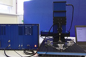
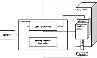
A typical scanning Kelvin probe (SKP) instrument. On the left is the control unit with lock-in amplifier and backing potential controller. On the right is the x, y, z scanning axis with vibrator, electrometer and probe mounted.

Kelvin probe force microscopy (KPFM), also known as surface potential microscopy, is a noncontact variant of atomic force microscopy (AFM). By raster scanning in the x,y plane the work function of the sample can be locally mapped for correlation with sample features. When there is little or no magnification, this approach can be described as using a scanning Kelvin probe (SKP). These techniques are predominantly used to measure corrosion and coatings.

With KPFM, the work function of surfaces can be observed at atomic or molecular scales. The work function relates to many surface phenomena, including catalytic activity, reconstruction of surfaces, doping and band-bending of semiconductors, charge trapping in dielectrics and corrosion. The map of the work function produced by KPFM gives information about the composition and electronic state of the local structures on the surface of a solid.

History

The SKP technique is based on parallel plate capacitor experiments performed by Lord Kelvin in 1898. In the 1930s William Zisman built upon Lord Kelvin's experiments to develop a technique to measure contact potential differences of dissimilar metals.

Working principle

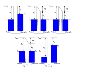
Diagram of Fermi level changes during scanning Kelvin probe
The changes to the Fermi levels of the scanning Kelvin probe (SKP) sample and probe during measurement are shown. On the electrical connection of the probe and sample their Fermi levels equilibrate, and a charge develops at the probe and sample. A backing potential is applied to null this charge, returning the sample Fermi level to its original position.

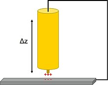
In SKP the probe and sample are held parallel to each other and electrically connected to form a parallel plate capacitor. The probe is selected to be of a different material to the sample, therefore each component initially has a distinct Fermi level. When electrical connection is made between the probe and the sample electron flow can occur between the probe and the sample in the direction of the higher to the lower Fermi level. This electron flow causes the equilibration of the probe and sample Fermi levels. Furthermore, a surface charge develops on the probe and the sample, with a related potential difference known as the contact potential (Vc). In SKP the probe is vibrated along a perpendicular to the plane of the sample. This vibration causes a change in probe to sample distance, which in turn results in the flow of current, taking the form of an ac sine wave. The resulting ac sine wave is demodulated to a dc signal through the use of a lock-in amplifier. Typically the user must select the correct reference phase value used by the lock-in amplifier. Once the dc potential has been determined, an external potential, known as the backing potential (Vb) can be applied to null the charge between the probe and the sample. When the charge is nullified, the Fermi level of the sample returns to its original position. This means that Vb is equal to -Vc, which is the work function difference between the SKP probe and the sample measured.

Illustration of scanning Kelvin probe
Simplified illustration of the scanning Kelvin probe (SKP) technique. The probe is shown to vibrate in z, perpendicular to the sample plane. The probe and sample form a parallel plate capacitor as shown.
 
Block diagram of scanning Kelvin probe
Block diagram of a scanning Kelvin probe (SKP) instrument showing computer, control unit, scan axes, vibrator, probe, and sample

The cantilever in the AFM is a reference electrode that forms a capacitor with the surface, over which it is scanned laterally at a constant separation. The cantilever is not piezoelectrically driven at its mechanical resonance frequency ω0 as in normal AFM although an alternating current (AC) voltage is applied at this frequency.

When there is a direct-current (DC) potential difference between the tip and the surface, the AC+DC voltage offset will cause the cantilever to vibrate. The origin of the force can be understood by considering that the energy of the capacitor formed by the cantilever and the surface is

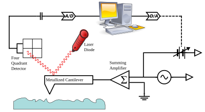
plus terms at DC. Only the cross-term proportional to the VDC·VAC product is at the resonance frequency ω0. The resulting vibration of the cantilever is detected using usual scanned-probe microscopy methods (typically involving a diode laser and a four-quadrant detector). A null circuit is used to drive the DC potential of the tip to a value which minimizes the vibration. A map of this nulling DC potential versus the lateral position coordinate therefore produces an image of the work function of the surface.

A related technique, electrostatic force microscopy (EFM), directly measures the force produced on a charged tip by the electric field emanating from the surface. EFM operates much like magnetic force microscopy in that the frequency shift or amplitude change of the cantilever oscillation is used to detect the electric field. However, EFM is much more sensitive to topographic artifacts than KPFM. Both EFM and KPFM require the use of conductive cantilevers, typically metal-coated silicon or silicon nitride. Another AFM-based technique for the imaging of electrostatic surface potentials, scanning quantum dot microscopy, quantifies surface potentials based on their ability to gate a tip-attached quantum dot.

Factors affecting SKP measurements

The quality of an SKP measurement is affected by a number of factors. This includes the diameter of the SKP probe, the probe to sample distance, and the material of the SKP probe. The probe diameter is important in the SKP measurement because it affects the overall resolution of the measurement, with smaller probes leading to improved resolution. On the other hand, reducing the size of the probe causes an increase in fringing effects which reduces the sensitivity of the measurement by increasing the measurement of stray capacitances. The material used in the construction of the SKP probe is important to the quality of the SKP measurement. This occurs for a number of reasons. Different materials have different work function values which will affect the contact potential measured. Different materials have different sensitivity to humidity changes. The material can also affect the resulting lateral resolution of the SKP measurement. In commercial probes tungsten is used, though probes of platinum, copper, gold, and NiCr has been used. The probe to sample distance affects the final SKP measurement, with smaller probe to sample distances improving the lateral resolution  and the signal-to-noise ratio of the measurement. Furthermore, reducing the SKP probe to sample distance increases the intensity of the measurement, where the intensity of the measurement is proportional to 1/d2, where d is the probe to sample distance. The effects of changing probe to sample distance on the measurement can be counteracted by using SKP in constant distance mode.

Work function

The Kelvin probe force microscope or Kelvin force microscope (KFM) is based on an AFM set-up and the determination of the work function is based on the measurement of the electrostatic forces between the small AFM tip and the sample. The conducting tip and the sample are characterized by (in general) different work functions, which represent the difference between the Fermi level and the vacuum level for each material. If both elements were brought in contact, a net electric current would flow between them until the Fermi levels were aligned. The difference between the work functions is called the contact potential difference and is denoted generally with VCPD. An electrostatic force exists between tip and sample, because of the electric field between them. For the measurement a voltage is applied between tip and sample, consisting of a DC-bias VDC and an AC-voltage VAC sin(ωt) of frequency ω.

Tuning the AC-frequency to the resonant frequency of the AFM cantilever results in an improved sensitivity. The electrostatic force in a capacitor may be found by differentiating the energy function with respect to the separation of the elements and can be written as

where C is the capacitance, z is the separation, and V is the voltage, each between tip and surface. Substituting the previous formula for voltage (V) shows that the electrostatic force can be split up into three contributions, as the total electrostatic force F acting on the tip then has spectral components at the frequencies ω and .

The DC component, FDC, contributes to the topographical signal, the term Fω at the characteristic frequency ω is used to measure the contact potential and the contribution F can be used for capacitance microscopy.

Contact potential measurements

For contact potential measurements a lock-in amplifier is used to detect the cantilever oscillation at ω. During the scan VDC will be adjusted so that the electrostatic forces between the tip and the sample become zero and thus the response at the frequency ω becomes zero. Since the electrostatic force at ω depends on VDC − VCPD, the value of VDC that minimizes the ω-term corresponds to the contact potential. Absolute values of the sample work function can be obtained if the tip is first calibrated against a reference sample of known work function. Apart from this, one can use the normal topographic scan methods at the resonance frequency ω independently of the above. Thus, in one scan, the topography and the contact potential of the sample are determined simultaneously. This can be done in (at least) two different ways: 1) The topography is captured in AC mode which means that the cantilever is driven by a piezo at its resonant frequency. Simultaneously the AC voltage for the KPFM measurement is applied at a frequency slightly lower than the resonant frequency of the cantilever. In this measurement mode the topography and the contact potential difference are captured at the same time and this mode is often called single-pass. 2) One line of the topography is captured either in contact or AC mode and is stored internally. Then, this line is scanned again, while the cantilever remains on a defined distance to the sample without a mechanically driven oscillation but the AC voltage of the KPFM measurement is applied and the contact potential is captured as explained above. It is important to note that the cantilever tip must not be too close to the sample in order to allow good oscillation with applied AC voltage. Therefore, KPFM can be performed simultaneously during AC topography measurements but not during contact topography measurements.

Applications

The Volta potential measured by SKP is directly proportional to the corrosion potential of a material, as such SKP has found widespread use in the study of the fields of corrosion and coatings. In the field of coatings for example, a scratched region of a self-healing shape memory polymer coating containing a heat generating agent on aluminium alloys was measured by SKP. Initially after the scratch was made the Volta potential was noticeably higher and wider over the scratch than over the rest of the sample, implying this region is more likely to corrode. The Volta potential decreased over subsequent measurements, and eventually the peak over the scratch completely disappeared implying the coating has healed. Because SKP can be used to investigate coatings in a non-destructive way it has also been used to determine coating failure. In a study of polyurethane coatings, it was seen that the work function increases with increasing exposure to high temperature and humidity. This increase in work function is related to decomposition of the coating likely from hydrolysis of bonds within the coating.

Using SKP the corrosion of industrially important alloys has been measured. In particular with SKP it is possible to investigate the effects of environmental stimulus on corrosion. For example, the microbially induced corrosion of stainless steel and titanium has been examined. SKP is useful to study this sort of corrosion because it usually occurs locally, therefore global techniques are poorly suited. Surface potential changes related to increased localized corrosion were shown by SKP measurements. Furthermore, it was possible to compare the resulting corrosion from different microbial species. In another example SKP was used to investigate biomedical alloy materials, which can be corroded within the human body. In studies on Ti-15Mo under inflammatory conditions, SKP measurements showed a lower corrosion resistance at the bottom of a corrosion pit than at the oxide protected surface of the alloy. SKP has also been used to investigate the effects of atmospheric corrosion, for example to investigate copper alloys in marine environment. In this study Kelvin potentials became more positive, indicating a more positive corrosion potential, with increased exposure time, due to an increase in thickness of corrosion products. As a final example SKP was used to investigate stainless steel under simulated conditions of gas pipeline. These measurements showed an increase in difference in corrosion potential of cathodic and anodic regions with increased corrosion time, indicating a higher likelihood of corrosion. Furthermore, these SKP measurements provided information about local corrosion, not possible with other techniques.

SKP has been used to investigate the surface potential of materials used in solar cells, with the advantage that it is a non-contact, and therefore a non-destructive technique. It can be used to determine the electron affinity of different materials in turn allowing the energy level overlap of conduction bands of differing materials to be determined. The energy level overlap of these bands is related to the surface photovoltage response of a system.

As a non-contact, non-destructive technique SKP has been used to investigate latent fingerprints on materials of interest for forensic studies. When fingerprints are left on a metallic surface they leave behind salts which can cause the localized corrosion of the material of interest. This leads to a change in Volta potential of the sample, which is detectable by SKP. SKP is particularly useful for these analyses because it can detect this change in Volta potential even after heating, or coating by, for example, oils.

SKP has been used to analyze the corrosion mechanisms of schreibersite-containing meteorites. The aim of these studies has been to investigate the role in such meteorites in releasing species utilized in prebiotic chemistry.

In the field of biology SKP has been used to investigate the electric fields associated with wounding, and acupuncture points.

In the field of electronics, KPFM is used to investigate the charge trapping in High-k gate oxides/interfaces of electronic devices.

Operator (computer programming)

From Wikipedia, the free encyclopedia https://en.wikipedia.org/wiki/Operator_(computer_programmin...