Search This Blog

Sunday, November 25, 2018

Integrated circuit design

From Wikipedia, the free encyclopedia

Layout view of a simple CMOS Operational Amplifier (inputs are to the left and the compensation capacitor is to the right). The metal layer is coloured blue, green and brown are N- and P-doped Si, the polysilicon is red and vias are crosses.

Integrated circuit design, or IC design, is a subset of electronics engineering, encompassing the particular logic and circuit design techniques required to design integrated circuits, or ICs. ICs consist of miniaturized electronic components built into an electrical network on a monolithic semiconductor substrate by photolithography.

IC design can be divided into the broad categories of digital and analog IC design. Digital IC design is to produce components such as microprocessors, FPGAs, memories (RAM, ROM, and flash) and digital ASICs. Digital design focuses on logical correctness, maximizing circuit density, and placing circuits so that clock and timing signals are routed efficiently. Analog IC design also has specializations in power IC design and RF IC design. Analog IC design is used in the design of op-amps, linear regulators, phase locked loops, oscillators and active filters. Analog design is more concerned with the physics of the semiconductor devices such as gain, matching, power dissipation, and resistance. Fidelity of analog signal amplification and filtering is usually critical and as a result, analog ICs use larger area active devices than digital designs and are usually less dense in circuitry.

Modern ICs are enormously complicated. An average desktop computer chip, as of 2015, has over 1 billion transistors. The rules for what can and cannot be manufactured are also extremely complex. Common IC processes of 2015 have more than 500 rules. Furthermore, since the manufacturing process itself is not completely predictable, designers must account for its statistical nature. The complexity of modern IC design, as well as market pressure to produce designs rapidly, has led to the extensive use of automated design tools in the IC design process. In short, the design of an IC using EDA software is the design, test, and verification of the instructions that the IC is to carry out.

Fundamentals

Integrated circuit design involves the creation of electronic components, such as transistors, resistors, capacitors and the metallic interconnect of these components onto a piece of semiconductor, typically silicon. A method to isolate the individual components formed in the substrate is necessary since the substrate silicon is conductive and often forms an active region of the individual components. The two common methods are p-n junction isolation and dielectric isolation. Attention must be given to power dissipation of transistors and interconnect resistances and current density of the interconnect, contacts and vias since ICs contain very tiny devices compared to discrete components, where such concerns are less of an issue. Electromigration in metallic interconnect and ESD damage to the tiny components are also of concern. Finally, the physical layout of certain circuit subblocks is typically critical, in order to achieve the desired speed of operation, to segregate noisy portions of an IC from quiet portions, to balance the effects of heat generation across the IC, or to facilitate the placement of connections to circuitry outside the IC.

Design steps

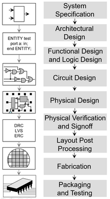
Major steps in the IC design flow

A typical IC design cycle involves several steps:
  1. System Specification
    1. Feasibility study and die size estimate
    2. Function analysis
  2. Architectural or System Level Design
  3. Logic Design
    1. Analogue Design, Simulation & Layout
    2. Digital Design & Simulation
    3. System Simulation & Verification
  4. Circuit Design
    1. Digital design synthesis
    2. Design For Test and Automatic test pattern generation
    3. Design for manufacturability (IC)
  5. Physical Design
    1. Floor planning
    2. Place and Route
    3. Parasitic Extraction
  6. Physical Verification & Signoff
    1. Static timing
    2. Co-simulation and timing
    3. Tape-in
    4. Mask data preparation
    5. Tape-out
  7. Wafer fabrication
  8. Packaging
  9. Die test
    1. Post silicon validation and integration
    2. Device characterization
    3. Tweak (if necessary)
  10. Chip Deployment
    1. Datasheet generation (of usually a Portable Document Format (PDF) file)
    2. Ramp up
    3. Production
    4. Yield Analysis / Warranty Analysis Reliability (semiconductor)
    5. Failure analysis on any returns
    6. Plan for next generation chip using production information if possible
Roughly saying, digital IC design can be divided into three parts.
  1. Electronic system-level design: This step creates the user functional specification. The user may use a variety of languages and tools to create this description. Examples include a C/C++ model, SystemC, SystemVerilog Transaction Level Models, Simulink and MATLAB;
  2. RTL design: This step converts the user specification (what the user wants the chip to do) into a register transfer level (RTL) description. The RTL describes the exact behavior of the digital circuits on the chip, as well as the interconnections to inputs and outputs;
  3. Physical design: This step takes the RTL, and a library of available logic gates, and creates a chip design. This involves figuring out which gates to use, defining places for them, and wiring them together.
Note that the second step, RTL design, is responsible for the chip doing the right thing. The third step, physical design, does not affect the functionality at all (if done correctly) but determines how fast the chip operates and how much it costs.

Design lifecycle

The integrated circuit (IC) development process starts with defining product requirements, progresses through architectural definition, implementation, bringup and finally productization. The various phases of the integrated circuit development process are described below. Although the phases are presented here in a straightforward fashion, in reality there is iteration and these steps may occur multiple times.

Requirements

Before an architecture can be defined some high level product goals must be defined. The requirements are usually generated by a cross functional team that addresses market opportunity, customer needs, feasibility and much more. This phase should result in a product requirements document.

Architecture

The architecture defines the fundamental structure, goals and principles of the product. It defines high level concepts and the intrinsic value proposition of the product. Architecture teams take into account many variables and interface with many groups. People creating the architecture generally have a significant amount of experience dealing with systems in the area for which the architecture is being created. The work product of the architecture phase is an architectural specification.

Micro-architecture

The micro-architecture is a step closer to the hardware. It implements the architecture and defines specific mechanisms and structures for achieving that implementation. The result of the micro-architecture phase is a micro-architecture specification which describes the methods used to implement the architecture.

Implementation

In the implementation phase the design itself is created using the micro-architectural specification as the starting point. This involves low level definition and partitioning, writing code, entering schematics and verification. This phase ends with a design reaching tapeout.

Bringup

After a design is created, taped-out and manufactured, actual hardware, 'first silicon', is received which is taken into the lab where it goes through bringup. Bringup is the process of powering, testing and characterizing the design in the lab. Numerous tests are performed starting from very simple tests such as ensuring that the device will power on to much more complicated tests which try to stress the part in various ways. The result of the bringup phase is documentation of characterization data (how well the part performs to spec) and errata (unexpected behavior).

Productization

Productization is the task of taking a design from engineering into mass production manufacturing. Although a design may have successfully met the specifications of the product in the lab during the bringup phase there are many challenges that face product engineers when trying to mass-produce those designs. The IC must be ramped up to production volumes with an acceptable yield. The goal of the productization phase is to reach mass production volumes at an acceptable cost.

Sustaining

Once a design is mature and has reached mass production it must be sustained. The process must be continually monitored and problems dealt with quickly to avoid a significant impact on production volumes. The goal of sustaining is to maintain production volumes and continually reduce costs until the product reaches end of life.

Design process

Microarchitecture and system-level design

The initial chip design process begins with system-level design and microarchitecture planning. Within IC design companies, management and often analytics will draft a proposal for a design team to start the design of a new chip to fit into an industry segment. Upper-level designers will meet at this stage to decide how the chip will operate functionally. This step is where an IC's functionality and design are decided. IC designers will map out the functional requirements, verification testbenches, and testing methodologies for the whole project, and will then turn the preliminary design into a system-level specification that can be simulated with simple models using languages like C++ and MATLAB and emulation tools. For pure and new designs, the system design stage is where an Instruction set and operation is planned out, and in most chips existing instruction sets are modified for newer functionality. Design at this stage is often statements such as encodes in the MP3 format or implements IEEE floating-point arithmetic. At later stages in the design process, each of these innocent looking statements expands to hundreds of pages of textual documentation.

RTL design

Upon agreement of a system design, RTL designers then implement the functional models in a hardware description language like Verilog, SystemVerilog, or VHDL. Using digital design components like adders, shifters, and state machines as well as computer architecture concepts like pipelining, superscalar execution, and branch prediction, RTL designers will break a functional description into hardware models of components on the chip working together. Each of the simple statements described in the system design can easily turn into thousands of lines of RTL code, which is why it is extremely difficult to verify that the RTL will do the right thing in all the possible cases that the user may throw at it.

To reduce the number of functionality bugs, a separate hardware verification group will take the RTL and design testbenches and systems to check that the RTL actually is performing the same steps under many different conditions, classified as the domain of functional verification. Many techniques are used, none of them perfect but all of them useful – extensive logic simulation, formal methods, hardware emulation, lint-like code checking, code coverage, and so on.

A tiny error here can make the whole chip useless, or worse. The famous Pentium FDIV bug caused the results of a division to be wrong by at most 61 parts per million, in cases that occurred very infrequently. No one even noticed it until the chip had been in production for months. Yet Intel was forced to offer to replace, for free, every chip sold until they could fix the bug, at a cost of $475 million (US).

Physical design

Physical design steps within the digital design flow

RTL is only a behavioral model of the actual functionality of what the chip is supposed to operate under. It has no link to a physical aspect of how the chip would operate in real life at the materials, physics, and electrical engineering side. For this reason, the next step in the IC design process, physical design stage, is to map the RTL into actual geometric representations of all electronics devices, such as capacitors, resistors, logic gates, and transistors that will go on the chip.

The main steps of physical design are listed below. In practice there is not a straightforward progression - considerable iteration is required to ensure all objectives are met simultaneously. This is a difficult problem in its own right, called design closure.
  1. Logic synthesis: The RTL is mapped into a gate-level netlist in the target technology of the chip;
  2. Floorplanning: The RTL of the chip is assigned to gross regions of the chip, input/output (I/O) pins are assigned and large objects (arrays, cores, etc.) are placed;
  3. Placement: The gates in the netlist are assigned to nonoverlapping locations on the die area.
  4. Logic/placement refinement: Iterative logical and placement transformations to close performance and power constraints;
  5. Clock insertion: Clock signal wiring is (commonly, clock trees) introduced into the design.
  6. Routing: The wires that connect the gates in the netlist are added;
  7. Postwiring optimization: Performance (timing closure), noise (signal integrity), and yield (Design for manufacturability) violations are removed;
  8. Design for manufacturability: The design is modified, where possible, to make it as easy and efficient as possible to produce. This is achieved by adding extra vias or adding dummy metal/diffusion/poly layers wherever possible while complying to the design rules set by the foundry;
  9. Final checking: Since errors are expensive, time consuming and hard to spot, extensive error checking is the rule, making sure the mapping to logic was done correctly, and checking that the manufacturing rules were followed faithfully;
  10. Tapeout and mask generation: the design data is turned into photomasks in mask data preparation.

Analog design

Before the advent of the microprocessor and software based design tools, analog ICs were designed using hand calculations and process kit parts. These ICs were low complexity circuits, for example, op-amps, usually involving no more than ten transistors and few connections. An iterative trial-and-error process and "overengineering" of device size was often necessary to achieve a manufacturable IC. Reuse of proven designs allowed progressively more complicated ICs to be built upon prior knowledge. When inexpensive computer processing became available in the 1970s, computer programs were written to simulate circuit designs with greater accuracy than practical by hand calculation. The first circuit simulator for analog ICs was called SPICE (Simulation Program with Integrated Circuits Emphasis). Computerized circuit simulation tools enable greater IC design complexity than hand calculations can achieve, making the design of analog ASICs practical. The computerized circuit simulators also enable mistakes to be found early in the design cycle before a physical device is fabricated. Additionally, a computerized circuit simulator can implement more sophisticated device models and circuit analysis too tedious for hand calculations, permitting Monte Carlo analysis and process sensitivity analysis to be practical. The effects of parameters such as temperature variation, doping concentration variation and statistical process variations can be simulated easily to determine if an IC design is manufacturable. Overall, computerized circuit simulation enables a higher degree of confidence that the circuit will work as expected upon manufacture.

Coping with variability

A challenge most critical to analog IC design involves the variability of the individual devices built on the semiconductor chip. Unlike board-level circuit design which permits the designer to select devices that have each been tested and binned according to value, the device values on an IC can vary widely which are uncontrollable by the designer. For example, some IC resistors can vary ±20% and β of an integrated BJT can vary from 20 to 100. In the latest CMOS processes, β of vertical PNP transistors can even go below 1. To add to the design challenge, device properties often vary between each processed semiconductor wafer. Device properties can even vary significantly across each individual IC due to doping gradients. The underlying cause of this variability is that many semiconductor devices are highly sensitive to uncontrollable random variances in the process. Slight changes to the amount of diffusion time, uneven doping levels, etc. can have large effects on device properties.

Some design techniques used to reduce the effects of the device variation are:
  • Using the ratios of resistors, which do match closely, rather than absolute resistor value.
  • Using devices with matched geometrical shapes so they have matched variations;
  • Making devices large so that statistical variations becomes an insignificant fraction of the overall device property;
  • Segmenting large devices, such as resistors, into parts and interweaving them to cancel variations;
  • Using common centroid device layout to cancel variations in devices which must match closely (such as the transistor differential pair of an op amp).

Vendors

The three largest companies selling electronic design automation tools are Synopsys, Cadence, and Mentor Graphics.

The Dunning-Kruger Effect May Help Explain Trump's Support

A new study suggests some people grossly overestimate their political knowledge.

Posted Aug 22, 2018
Original link:  https://www.psychologytoday.com/us/blog/mind-in-the-machine/201808/the-dunning-kruger-effect-may-help-explain-trumps-support

Elvert Barnes Photography/Flickr
Source: Elvert Barnes Photography/Flickr

In the past, some prominent psychologists have explained President Donald Trump’s unwavering support by alluding to a well-established psychological phenomenon known as the “Dunning-Kruger effect.” The effect is a type of cognitive bias, where people with little expertise or ability assume they have superior expertise or ability. This overestimation occurs as a result of the fact that they don’t have enough knowledge to know they don’t have enough knowledge. This simple but loopy concept has been demonstrated dozens of times in well-controlled psychology studies and in a variety of contexts. However, until now, the effect had not been studied in one of the most obvious and important realms—political knowledge.

new study published in the journal Political Psychology, carried out by the political scientist Ian Anson at the University of Maryland Baltimore County, not only found that the Dunning-Kruger effect applies to politics, it also appears to be exacerbated when partisan identities are made more salient. In other words, those who score low on political knowledge tend to overestimate their expertise even more when greater emphasis is placed on political affiliation.

Anson told PsyPost that he became increasingly interested in the effect after other academics were discussing its potential role in the 2016 U.S. presidential election on social media. “I follow a number of political scientists who marveled at the social media pundit class’ seeming display of ‘Dunning-Kruger-ish tendencies’ in their bombastic coverage of the election.” However, speculation by scientists does not always translate into statistically-significant findings, so Anson began thinking of ways to experimentally test what he described as a “very serious accusation.”

In order to have a large representative sample of subjects, Dr. Anson administered online surveys to over 2,600 Americans. The first survey was designed to assess political knowledge, while the second was used to examine how confident they were in their knowledge. Questions quizzed participants on topics like names of cabinet members, the length of term limits for members of Congress, and the names of programs that the U.S. government spends the least on.

As predicted, the results showed that those who scored low on political knowledge were also the ones who overestimated their level of knowledge. But that wasn’t all. When participants were given cues that made them engage in partisan thought, the Dunning-Kruger effect was made even stronger. This occurred with both Republicans and Democrats, but only in those who scored low on political knowledge to begin with.

These findings are fascinating but equally troubling. How do you combat ignorance when the ignorant believe themselves to be knowledgeable? Even worse, how do you fight it when America is becoming increasingly polarized, which certainly increases the salience of partisan identities?

While the results of Anson’s study suggest that being uninformed leads to overconfidence across the political spectrum, studies have shown that Democrats now tend to be generally more educated than Republicans, possibly making the latter more vulnerable to the Dunning-Kruger effect. In fact, a Pew Research Center poll released in March of this year found that 54 percent of college graduates identified as Democrats or leaned Democratic, compared to 39 percent who identified or leaned Republican.

This effect may help explain why certain Trump supporters seem to be so easily tricked into believing proven falsehoods when the President delivers what have become known as “alternative facts,” often using language designed to activate partisan identities. Because they lack knowledge but are confident that they do not, they may be less likely than others to actually fact-check the claims that the President makes.

This speculation is supported by evidence from empirical studies. In 2016, an experiment found that 45 percent of Republicans believed that the Affordable Care Act included “death panels,” and a 2015 study similarly found that 54 percent of Republican primary voters believed then-president Barack Obama to be a Muslim.

The Dunning-Kruger effect is particularly worrisome when considering issues that pose existential threats, like global warming. A 2017 study conducted at the University of New Hampshire, for instance, found that only 25 percent of self-described Trump supporters believed that human activities contribute to climate change—though 97 percent of scientists who study climate change agree that they do.

This quirky cognitive bias could potentially be making it easier for Donald Trump to say unchallenged falsehoods to his more uneducated followers. In some cases, not only are these individuals uninformed, they are unlikely to ever try to become more informed on their own. In their minds, they have nothing new to learn.

While such a thought is disturbing, we should not lose all hope in trying to reach the victims of the Dunning-Kruger effect. At least one study found that incompetent students increased their ability to accurately estimate their class rank after being tutored in the skills they lacked. With the right education methods and a willingness to learn, the uninformed on both sides of the political aisle can gain a meta-awareness that can help them perceive themselves more objectively.

Unfortunately, Anson’s study shows that getting through to these people becomes more and more difficult as the nation becomes more divided. And with Trump’s fiery rhetoric and fear-mongering, that divide appears to always be growing wider.

Electronic design automation

From Wikipedia, the free encyclopedia

Electronic design automation (EDA), also referred to as electronic computer-aided design (ECAD), is a category of software tools for designing electronic systems such as integrated circuits and printed circuit boards. The tools work together in a design flow that chip designers use to design and analyze entire semiconductor chips. Since a modern semiconductor chip can have billions of components, EDA tools are essential for their design.

This article describes EDA specifically with respect to integrated circuits.

History

Early days

Before EDA, integrated circuits were designed by hand, and manually laid out. Some advanced shops used geometric software to generate the tapes for the Gerber photoplotter, but even those copied digital recordings of mechanically drawn components. The process was fundamentally graphic, with the translation from electronics to graphics done manually. The best known company from this era was Calma, whose GDSII format survives.

By the mid-1970s, developers started to automate the design along with the drafting. The first placement and routing (Place and route) tools were developed. The proceedings of the Design Automation Conference cover much of this era.

The next era began about the time of the publication of "Introduction to VLSI Systems" by Carver Mead and Lynn Conway in 1980. This ground breaking text advocated chip design with programming languages that compiled to silicon. The immediate result was a considerable increase in the complexity of the chips that could be designed, with improved access to design verification tools that used logic simulation. Often the chips were easier to lay out and more likely to function correctly, since their designs could be simulated more thoroughly prior to construction. Although the languages and tools have evolved, this general approach of specifying the desired behavior in a textual programming language and letting the tools derive the detailed physical design remains the basis of digital IC design today.

The earliest EDA tools were produced academically. One of the most famous was the "Berkeley VLSI Tools Tarball", a set of UNIX utilities used to design early VLSI systems. Still widely used are the Espresso heuristic logic minimizer and Magic.

Another crucial development was the formation of MOSIS, a consortium of universities and fabricators that developed an inexpensive way to train student chip designers by producing real integrated circuits. The basic concept was to use reliable, low-cost, relatively low-technology IC processes, and pack a large number of projects per wafer, with just a few copies of each projects' chips. Cooperating fabricators either donated the processed wafers, or sold them at cost, seeing the program as helpful to their own long-term growth.

Birth of commercial EDA

1981 marks the beginning of EDA as an industry. For many years, the larger electronic companies, such as Hewlett Packard, Tektronix, and Intel, had pursued EDA internally. In 1981, managers and developers spun out of these companies to concentrate on EDA as a business. Daisy Systems, Mentor Graphics, and Valid Logic Systems were all founded around this time, and collectively referred to as DMV. Within a few years there were many companies specializing in EDA, each with a slightly different emphasis. The first trade show for EDA was held at the Design Automation Conference in 1984.

In 1981, the U.S. Department of Defense began funding of VHDL as a hardware description language. In 1986, Verilog, another popular high-level design language, was first introduced as a hardware description language by Gateway Design Automation. Simulators quickly followed these introductions, permitting direct simulation of chip designs: executable specifications. In a few more years, back-ends were developed to perform logic synthesis.

Current status

Current digital flows are extremely modular (see Integrated circuit design, Design closure, and Design flow (EDA)). The front ends produce standardized design descriptions that compile into invocations of "cells,", without regard to the cell technology. Cells implement logic or other electronic functions using a particular integrated circuit technology. Fabricators generally provide libraries of components for their production processes, with simulation models that fit standard simulation tools. Analog EDA tools are far less modular, since many more functions are required, they interact more strongly, and the components are (in general) less ideal.

EDA for electronics has rapidly increased in importance with the continuous scaling of semiconductor technology.[2] Some users are foundry operators, who operate the semiconductor fabrication facilities, or "fabs", and design-service companies who use EDA software to evaluate an incoming design for manufacturing readiness. EDA tools are also used for programming design functionality into FPGAs.

Software focuses

Design

  • High-level synthesis (or behavioural synthesis, algorithmic synthesis) – high-level design description (e.g. in C/C++) is converted into RTL.
  • Logic synthesis – translation of RTL design description (e.g. written in Verilog or VHDL) into a discrete netlist of logic gates.
  • Schematic capture – For standard cell digital, analog, RF-like Capture CIS in Orcad by Cadence and ISIS in Proteus
  • Layout – usually schematic-driven layout, like Layout in Orcad by Cadence, ARES in Proteus

Simulation

  • Transistor simulation – low-level transistor-simulation of a schematic/layout's behavior, accurate at device-level.
  • Logic simulation – digital-simulation of an RTL or gate-netlist's digital (boolean 0/1) behavior, accurate at boolean-level.
  • Behavioral Simulation – high-level simulation of a design's architectural operation, accurate at cycle-level or interface-level.
  • Hardware emulation – Use of special purpose hardware to emulate the logic of a proposed design. Can sometimes be plugged into a system in place of a yet-to-be-built chip; this is called in-circuit emulation.
  • Technology CAD simulate and analyze the underlying process technology. Electrical properties of devices are derived directly from device physics.
  • Electromagnetic field solvers, or just field solvers, solve Maxwell's equations directly for cases of interest in IC and PCB design. They are known for being slower but more accurate than the layout extraction above.[where?]
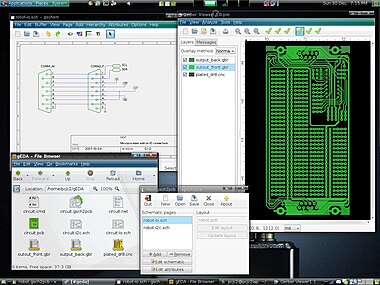
Schematic capture program

Analysis and verification

  • Functional verification
  • Clock Domain Crossing Verification (CDC check): Similar to linting, but these checks/tools specialize in detecting and reporting potential issues like data loss, meta-stability due to use of multiple clock domains in the design.
  • Formal verification, also model checking: Attempts to prove, by mathematical methods, that the system has certain desired properties, and that certain undesired effects (such as deadlock) cannot occur.
  • Equivalence checking: algorithmic comparison between a chip's RTL-description and synthesized gate-netlist, to ensure functional equivalence at the logical level.
  • Static timing analysis: Analysis of the timing of a circuit in an input-independent manner, hence finding a worst case over all possible inputs.
  • Physical verification, PV: checking if a design is physically manufacturable, and that the resulting chips will not have any function-preventing physical defects, and will meet original specifications.

Manufacturing preparation

Functional Safety

  • Functional Safety Analysis, Systematic computation of failure in time (FIT) rates and diagnostic coverage metrics for designs in order to meet the compliance requirements for the desired safety integrity levels.
  • Functional Safety Synthesis, Add reliability enhancements to structured elements (Modules, RAMs, ROMs, Register Files, FIFOs) to improves fault detection / fault tolerance. These includes (not limited to), Addition of error detection and / or correction codes (Hamming), Redundant logic for fault detection and fault tolerance (duplicate / triplicate) and Protocol checks (Interface parity, address alignment, beat count)
  • Functional Safety Verification,Running of a fault campaign, including insertion of faults into the design and verification that the safety mechanism reacts in an appropriate manner for the faults that are deemed covered.
PCB layout and schematic for connector design

Companies

Old companies

Market capitalization and company name as of December 2011:
Note: EEsof should likely be on this list, but it does not have a market cap as it is the EDA division of Keysight.

Acquisitions

Many of the EDA companies acquire small companies with software or other technology that can be adapted to their core business. Most of the market leaders are amalgamations of many smaller companies. This trend is helped by the tendency of software companies to design tools as accessories that fit naturally into a larger vendor's suite of programs on digital circuitry, many new tools incorporate analog design, and mixed systems. This is happening because there is now a trend to place entire electronic systems on a single chip.

LabVIEW

From Wikipedia, the free encyclopedia

LabVIEW
LabVIEW logo.
Developer(s)National Instruments
Initial release1986; 32 years ago
Stable release
LabVIEW NXG 2.1 LabVIEW 2018
/ May 2018; 6 months ago
Preview release
NXG 3.0 Beta1
Written inC, C++, .NET
Operating systemCross-platform: Windows, macOS, Linux
TypeData acquisition, instrument control, test automation, analysis and signal processing, industrial control, embedded system design
LicenseProprietary
Websitewww.ni.com/labview

Laboratory Virtual Instrument Engineering Workbench (LabVIEW) is a system-design platform and development environment for a visual programming language from National Instruments.

The graphical language is named "G"; not to be confused with G-code. Originally released for the Apple Macintosh in 1986, LabVIEW is commonly used for data acquisition, instrument control, and industrial automation on a variety of operating systems (OSs), including Microsoft Windows, various versions of Unix, Linux, and macOS.

The latest versions of LabVIEW are LabVIEW 2018 and LabVIEW NXG 2.1, released in May 2018.

Dataflow programming

The programming paradigm used in LabVIEW, sometimes called G, is based on data availability. If there is enough data available to a subVI or function, that subVI or function will execute. Execution flow is determined by the structure of a graphical block diagram (the LabVIEW-source code) on which the programmer connects different function-nodes by drawing wires. These wires propagate variables and any node can execute as soon as all its input data become available. Since this might be the case for multiple nodes simultaneously, LabVIEW can execute inherently in parallel. Multi-processing and multi-threading hardware is exploited automatically by the built-in scheduler, which multiplexes multiple OS threads over the nodes ready for execution.

Graphical programming

LabVIEW integrates the creation of user interfaces (termed front panels) into the development cycle. LabVIEW programs-subroutines are termed virtual instruments (VIs). Each VI has three components: a block diagram, a front panel, and a connector panel. The last is used to represent the VI in the block diagrams of other, calling VIs. The front panel is built using controls and indicators. Controls are inputs: they allow a user to supply information to the VI. Indicators are outputs: they indicate, or display, the results based on the inputs given to the VI. The back panel, which is a block diagram, contains the graphical source code. All of the objects placed on the front panel will appear on the back panel as terminals. The back panel also contains structures and functions which perform operations on controls and supply data to indicators. The structures and functions are found on the Functions palette and can be placed on the back panel. Collectively controls, indicators, structures, and functions are referred to as nodes. Nodes are connected to one another using wires, e.g., two controls and an indicator can be wired to the addition function so that the indicator displays the sum of the two controls. Thus a virtual instrument can be run as either a program, with the front panel serving as a user interface, or, when dropped as a node onto the block diagram, the front panel defines the inputs and outputs for the node through the connector panel. This implies each VI can be easily tested before being embedded as a subroutine into a larger program.

The graphical approach also allows nonprogrammers to build programs by dragging and dropping virtual representations of lab equipment with which they are already familiar. The LabVIEW programming environment, with the included examples and documentation, makes it simple to create small applications. This is a benefit on one side, but there is also a certain danger of underestimating the expertise needed for high-quality G programming. For complex algorithms or large-scale code, it is important that a programmer possess an extensive knowledge of the special LabVIEW syntax and the topology of its memory management. The most advanced LabVIEW development systems offer the ability to build stand-alone applications. Furthermore, it is possible to create distributed applications, which communicate by a client–server model, and are thus easier to implement due to the inherently parallel nature of G.

Widely-accepted design patterns

Applications in LabVIEW are usually designed using well-known architectures, known as design patterns. The most common design patterns for graphical LabVIEW applications are listed in the table below.

Common design patterns for LabVIEW applications
Design pattern Purpose Implementation details Use cases Limitations
Functional Global Variable Exchange information without using global variables A shift register of a while loop is used to store the data and the while loop runs only one iteration in a "non-reentrant" VI
  • Exchange information with less wiring
  • All owning VIs are kept in memory
State machine Controlled execution that depends on past events Case structure inside a while loop pass an enumerated variable to a shift register, representing the next state; complex state machines can be designed using the Statechart module
  • User interfaces
  • Complex logic
  • Communication protocols
  • All possible states must be known in advance
Event-driven user interface Lossless processing of user actions GUI events are captured by an event structure queue, inside a while loop; the while loop is suspended by the event structure and resumes only when the desired events are captured
  • Graphical user interface
  • Only one event structure in a loop
Master-slave[5] Run independent processes simultaneously Several parallel while loops, out of which one functions as the "master", controlling the "slave" loops
  • Simple GUI for data acquisition and visualization
Producer-consumer Asynchronous of multithreaded execution of loops A master loop controls the execution of two slave loops, that communicate using notifiers, queues and semaphores; data-independent loops are automatically executed in separate threads
  • Data sampling and visualization
  • Order of execution is not obvious to control
Queued state machine with event-driven producer-consumer Highly responsive user-interface for multithreaded applications An event-driven user interface is placed inside the producer loop and a state machine is placed inside the consumer loop, communicating using queues between themselves and other parallel VIs
  • Complex applications

Benefits

Interfacing to devices

LabVIEW includes extensive support for interfacing to devices, instruments, camera, and other devices. Users interface to hardware by either writing direct bus commands (USB, GPIB, Serial) or using high-level, device-specific, drivers that provide native LabVIEW function nodes for controlling the device.

LabVIEW includes built-in support for NI hardware platforms such as CompactDAQ and CompactRIO, with a large number of device-specific blocks for such hardware, the Measurement and Automation eXplorer (MAX) and Virtual Instrument Software Architecture (VISA) toolsets.

National Instruments makes thousands of device drivers available for download on the NI Instrument Driver Network (IDNet).

Code compiling

LabVIEW includes a compiler that produces native code for the CPU platform. This aids performance. The graphical code is translated into executable machine code by a compiler. The LabVIEW syntax is strictly enforced during the editing process and compiled into the executable machine code when requested to run or upon saving. In the latter case, the executable and the source code are merged into a single file. The executable runs with the help of the LabVIEW run-time engine, which contains some pre-compiled code to perform common tasks that are defined by the G language. The run-time engine reduces compiling time and provides a consistent interface to various operating systems, graphic systems, hardware components, etc. The run-time environment makes the code portable across platforms. Generally, LabVIEW code can be slower than equivalent compiled C code, although the differences often lie more with program optimization than inherent execution speed.

Large libraries

Many libraries with a large number of functions for data acquisition, signal generation, mathematics, statistics, signal conditioning, analysis, etc., along with numerous for functions such as integration, filters, and other specialized abilities usually associated with data capture from hardware sensors is enormous. In addition, LabVIEW includes a text-based programming component named MathScript with added functions for signal processing, analysis, and mathematics. MathScript can be integrated with graphical programming using script nodes and uses a syntax that is compatible generally with MATLAB.

Parallel programming

LabVIEW is an inherently concurrent language, so it is very easy to program multiple tasks that are performed in parallel via multithreading. For example, this is done easily by drawing two or more parallel while loops and connecting them to two separate nodes. This is a great benefit for test system automation, where it is common practice to run processes like test sequencing, data recording, and hardware interfacing in parallel.

Ecosystem

Due to the longevity and popularity of the LabVIEW language, and the ability for users to extend its functions, a large ecosystem of third party add-ons has developed via contributions from the community. This ecosystem is available on the LabVIEW Tools Network, which is a marketplace for both free and paid LabVIEW add-ons.

User community

There is a low-cost LabVIEW Student Edition aimed at educational institutions for learning purposes. There is also an active community of LabVIEW users who communicate through several electronic mailing lists (email groups) and Internet forums.

Home Bundle Edition

National Instruments provides a low cost LabVIEW Home Bundle Edition.

Criticism

LabVIEW is a proprietary product of National Instruments. Unlike common programming languages such as C or Fortran, LabVIEW is not managed or specified by a third party standards committee such as American National Standards Institute (ANSI), Institute of Electrical and Electronics Engineers (IEEE), International Organization for Standardization (ISO), etc.

Slow

Very small applications still have to start the runtime environment which is a large and slow task. This tends to restrict LabVIEW to monolithic applications. Examples of this might be tiny programs to grab a single value from some hardware that can be used in a scripting language - the overheads of the runtime environment render this approach impractical with LabVIEW.

Non-textual

G language being non-textual, software tools such as versioning, side-by-side (or diff) comparison, and version code change tracking cannot be applied in the same manner as for textual programming languages. There are some additional tools to make comparison and merging of code with source code control (versioning) tools such as subversion, CVS and Perforce. 

No zoom function

There was no ability to zoom in to (or enlarge) a VI which will be hard to see on a large, high-resolution monitor, although this feature was released as of 2017.

Release history

In 2005, starting with LabVIEW 8.0, major versions are released around the first week of August, to coincide with the annual National Instruments conference NI Week, and followed by a bug-fix release the following February.

In 2009, National Instruments began naming releases after the year in which they are released. A bug-fix is termed a Service Pack, for example, the 2009 service pack 1 was released in February 2010.

In 2017, National Instruments moved the annual conference to May and released LabVIEW 2017 along side a completely redesigned LabVIEW NXG 1.0 built on Windows Presentation Foundation (WPF).

Name-version Build number Date
LabVIEW project begins
April 1983
LabVIEW 1.0 (for Macintosh) ?? October 1986
LabVIEW 2.0 ?? January 1990
LabVIEW 2.5 (first release for Sun & Windows) ?? August 1992
LabVIEW 3.0 (Multiplatform) ?? July 1993
LabVIEW 3.0.1 (first release for Windows NT) ?? 1994
LabVIEW 3.1 ?? 1994
LabVIEW 3.1.1 (first release with "application builder" ability) ?? 1995
LabVIEW 4.0 ?? April 1996
LabVIEW 4.1 ?? 1997
LabVIEW 5.0 ?? February 1998
LabVIEW RT (Real Time) ?? May 1999
LabVIEW 6.0 (6i) 6.0.0.4005 26 July 2000
LabVIEW 6.1 6.1.0.4004 12 April 2001
LabVIEW 7.0 (Express) 7.0.0.4000 April 2003
LabVIEW PDA module first released ?? May 2003
LabVIEW FPGA module first released ?? June 2003
LabVIEW 7.1 7.1.0.4000 2004
LabVIEW Embedded module first released ?? May 2005
LabVIEW 8.0 8.0.0.4005 September 2005
LabVIEW 8.20 (native Object Oriented Programming) ?? August 2006
LabVIEW 8.2.1 8.2.1.4002 21 February 2007
LabVIEW 8.5 8.5.0.4002 2007
LabVIEW 8.6 8.6.0.4001 24 July 2008
LabVIEW 8.6.1 8.6.0.4001 10 December 2008
LabVIEW 2009 (32 and 64-bit) 9.0.0.4022 4 August 2009
LabVIEW 2009 SP1 9.0.1.4011 8 January 2010
LabVIEW 2010 10.0.0.4032 4 August 2010
LabVIEW 2010 f2 10.0.0.4033 16 September 2010
LabVIEW 2010 SP1 10.0.1.4004 17 May 2011
LabVIEW for LEGO MINDSTORMS (2010 SP1 with some modules)
August 2011
LabVIEW 2011 11.0.0.4029 22 June 2011
LabVIEW 2011 SP1 11.0.1.4015 1 March 2012
LabVIEW 2012 12.0.0.4029 August 2012
LabVIEW 2012 SP1 12.0.1.4013 December 2012
LabVIEW 2013 13.0.0.4047 August 2013
LabVIEW 2013 SP1 13.0.1.4017 March 2014
LabVIEW 2014
August 2014
LabVIEW 2014 SP1 14.0.1.4008 March 2015
LabVIEW 2015 15.0f2 August 2015
LabVIEW 2015 SP1 15.0.1f1 March 2016
LabVIEW 2016 16.0.0 August 2016
LabVIEW 2017 17.0f1 May 2017
LabVIEW 2017 SP1 17.0.1f1 Jan 2018 
LabVIEW 2018 18.0 May 2018

Repositories and libraries

OpenG, as well as LAVA Code Repository (LAVAcr), serve as repositories for a wide range of Open Source LabVIEW applications and libraries. SourceForge has LabVIEW listed as one of the possible languages in which code can be written.

VI Package Manager has become the standard package manager for LabVIEW libraries. It is very similar in purpose to Ruby's RubyGems and Perl's CPAN, although it provides a graphical user interface similar to the Synaptic Package Manager. VI Package Manager provides access to a repository of the OpenG (and other) libraries for LabVIEW.

Tools exist to convert MathML into G code.

Related software

National Instruments also offers a product named Measurement Studio, which offers many of the test, measurement, and control abilities of LabVIEW, as a set of classes for use with Microsoft Visual Studio. This allows developers to harness some of LabVIEW's strengths within the text-based .NET Framework. National Instruments also offers LabWindows/CVI as an alternative for ANSI C programmers.

When applications need sequencing, users often use LabVIEW with TestStand test management software, also from National Instruments.

The Ch interpreter is a C/C++ interpreter that can be embedded in LabVIEW for scripting.

The TRIL Centre Ireland BioMobius platform and DSP Robotics' FlowStone DSP also use a form of graphical programming similar to LabVIEW, but are limited to the biomedical and robotics industries respectively.

LabVIEW has a direct node with modeFRONTIER, a multidisciplinary and multi-objective optimization and design environment, written to allow coupling to almost any computer-aided engineering tool. Both can be part of the same process workflow description and can be virtually driven by the optimization technologies available in modeFRONTIER.

Inequality (mathematics)

From Wikipedia, the free encyclopedia https://en.wikipedia.org/wiki/Inequality...