Search This Blog

Thursday, January 16, 2020

Gallium nitride

From Wikipedia, the free encyclopedia
https://en.wikipedia.org/wiki/Gallium_nitride
 
Gallium nitride
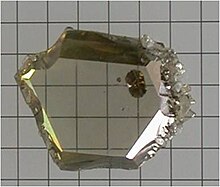
GaNcrystal.jpg
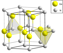
GaN Wurtzite polyhedra.png
Names
IUPAC name
Gallium nitride
Identifiers
3D model (JSmol)
ChemSpider
ECHA InfoCard 100.042.830
PubChem CID
Properties
GaN
Molar mass 83.730 g/mol
Appearance yellow powder
Density 6.1 g/cm3
Melting point >1600 °C
Insoluble
Band gap 3.4 eV (300 K, direct)
Electron mobility 1500 cm2/(V·s) (300 K)
Thermal conductivity 1.3 W/(cm·K) (300 K)
2.429
Structure
Wurtzite
C6v4-P63mc
a = 3.186 Å, c = 5.186 Å
Tetrahedral
Thermochemistry
−110.2 kJ/mol
Hazards
Flash point Non-flammable
Related compounds
Other anions
Gallium phosphide
Gallium arsenide
Gallium antimonide
Other cations
Boron nitride
Aluminium nitride
Indium nitride
Related compounds
Aluminium gallium arsenide
Indium gallium arsenide
Gallium arsenide phosphide
Aluminium gallium nitride
Indium gallium nitride
Except where otherwise noted, data are given for materials in their standard state (at 25 °C [77 °F], 100 kPa).
☑ verify (what is ☑☒ ?)
Infobox references

Gallium nitride (GaN) is a binary III/V direct bandgap semiconductor commonly used in light-emitting diodes since the 1990s. The compound is a very hard material that has a Wurtzite crystal structure. Its wide band gap of 3.4 eV affords it special properties for applications in optoelectronic, high-power and high-frequency devices. For example, GaN is the substrate which makes violet (405 nm) laser diodes possible, without use of nonlinear optical frequency-doubling.

Its sensitivity to ionizing radiation is low (like other group III nitrides), making it a suitable material for solar cell arrays for satellites. Military and space applications could also benefit as devices have shown stability in radiation environments.

Because GaN transistors can operate at much higher temperatures and work at much higher voltages than gallium arsenide (GaAs) transistors, they make ideal power amplifiers at microwave frequencies. In addition, GaN offers promising characteristics for THz devices.

Physical properties

GaN crystal

GaN is a very hard (12±2 GPa), mechanically stable wide bandgap semiconductor material with high heat capacity and thermal conductivity. In its pure form it resists cracking and can be deposited in thin film on sapphire or silicon carbide, despite the mismatch in their lattice constants. GaN can be doped with silicon (Si) or with oxygen to n-type and with magnesium (Mg) to p-type. However, the Si and Mg atoms change the way the GaN crystals grow, introducing tensile stresses and making them brittle. Gallium nitride compounds also tend to have a high dislocation density, on the order of 108 to 1010 defects per square centimeter. The wide band-gap behavior of GaN is connected to specific changes in the electronic band structure, charge occupation and chemical bond regions.

The U.S. Army Research Laboratory (ARL) provided the first measurement of the high field electron velocity in GaN in 1999. Scientists at ARL experimentally obtained a peak steady-state velocity of 1.9 x 107 cm/s, with a transit time of 2.5 picoseconds, attained at an electric field of 225 kV/cm. With this information, the electron mobility was calculated, thus providing data for the design of GaN devices. 

Developments

GaN with a high crystalline quality can be obtained by depositing a buffer layer at low temperatures. Such high-quality GaN led to the discovery of p-type GaN, p-n junction blue/UV-LEDs and room-temperature stimulated emission (essential for laser action). This has led to the commercialization of high-performance blue LEDs and long-lifetime violet-laser diodes, and to the development of nitride-based devices such as UV detectors and high-speed field-effect transistors.

LEDs

High-brightness GaN light-emitting diodes (LEDs) completed the range of primary colors, and made applications such as daylight visible full-color LED displays, white LEDs and blue laser devices possible. The first GaN-based high-brightness LEDs used a thin film of GaN deposited via Metal-Organic Vapour Phase Epitaxy (MOVPE) on sapphire. Other substrates used are zinc oxide, with lattice constant mismatch of only 2% and silicon carbide (SiC). Group III nitride semiconductors are, in general, recognized as one of the most promising semiconductor families for fabricating optical devices in the visible short-wavelength and UV region.

Transistors

The very high breakdown voltages, high electron mobility and saturation velocity of GaN has also made it an ideal candidate for high-power and high-temperature microwave applications, as evidenced by its high Johnson's figure of merit. Potential markets for high-power/high-frequency devices based on GaN include microwave radio-frequency power amplifiers (such as those used in high-speed wireless data transmission) and high-voltage switching devices for power grids. A potential mass-market application for GaN-based RF transistors is as the microwave source for microwave ovens, replacing the magnetrons currently used. The large band gap means that the performance of GaN transistors is maintained up to higher temperatures (~400 °C) than silicon transistors (~150 °C) because it lessens the effects of thermal generation of charge carriers that are inherent to any semiconductor. The first gallium nitride metal semiconductor field-effect transistors (GaN MESFET) were experimentally demonstrated in 1993 and they are being actively developed.

In 2010 the first enhancement-mode GaN transistors became generally available. Only n-channel transistors were available. These devices were designed to replace power MOSFETs in applications where switching speed or power conversion efficiency is critical. These transistors, also called eGaN FETs, are built by growing a thin layer of GaN on top of a standard silicon wafer. This allows the eGaN FETs to maintain costs similar to silicon power MOSFETs but with the superior electrical performance of GaN. 

Applications


LEDs

GaN-based violet laser diodes are used to read Blu-ray Discs. The mixture of GaN with In (InGaN) or Al (AlGaN) with a band gap dependent on ratio of In or Al to GaN allows the manufacture of light-emitting diodes (LEDs) with colors that can go from red to ultra-violet.

Transistors

GaN transistors are suitable for high frequency, high voltage, high temperature and high efficiency applications. 

GaN HEMTs have been offered commercially since 2006, and have found immediate use in various wireless infrastructure applications due to their high efficiency and high voltage operation. A second generation of devices with shorter gate lengths will address higher frequency telecom and aerospace applications.

GaN based MOSFET and MESFET transistors also offer advantages including lower loss in high power electronics, especially in automotive and electric car applications. Since 2008 these can be formed on a silicon substrate. High-voltage (800 V) Schottky barrier diodes (SBDs) have also been made.

GaN-based electronics (not pure GaN) has the potential to drastically cut energy consumption, not only in consumer applications but even for power transmission utilities.

Unlike silicon transistors which switch off due to power surges, GaN transistors are typically depletion mode devices (i.e. on / resistive when the gate-source voltage is zero). Several methods have been proposed to reach normally-off (or E-mode) operation, which is necessary for use in power electronics:
  • the implantation of fluorine ions under the gate (the negative charge of the F-ions favors the depletion of the channel)
  • the use of a MIS-type gate stack, with recess of the AlGaN
  • the integration of a cascaded pair constituted by a normally-on GaN transistor and a low voltage silicon MOSFET
  • the use of a p-type layer on top of the AlGaN/GaN heterojunction

Radars

They are also utilized in military electronics such as active electronically scanned array radars.

The U.S. Army funded Lockheed Martin to incorporate GaN active-device technology into the AN/TPQ-53 radar system to replace two medium-range radar systems, the AN/TPQ-36 and the AN/TPQ-37. The AN/TPQ-53 radar system was designed to detect, classify, track, and locate enemy indirect fire systems, as well as unmanned aerial systems. The AN/TPQ-53 radar system provided enhanced performance, greater mobility, increased reliability and supportability, lower life-cycle cost, and reduced crew size compared to the AN/TPQ-36 and the AN/TPQ-37 systems.

Lockheed Martin fielded other tactical operational radars with GaN technology in 2018, including TPS-77 Multi Role Radar System deployed to Latvia and Romania. In 2019, Lockheed Martin's partner ELTA Systems Limited, developed a GaN-based ELM-2084 Multi Mission Radar that was able to detect and track air craft and ballistic targets, while providing fire control guidance for missile interception or air defense artillery. 

Nanoscale

GaN nanotubes and nanowires are proposed for applications in nanoscale electronics, optoelectronics and biochemical-sensing applications.

Spintronics potential

When doped with a suitable transition metal such as manganese, GaN is a promising spintronics material (magnetic semiconductors).

Synthesis


Bulk substrates

GaN crystals can be grown from a molten Na/Ga melt held under 100 atmospheres of pressure of N2 at 750 °C. As Ga will not react with N2 below 1000 °C, the powder must be made from something more reactive, usually in one of the following ways:
2 Ga + 2 NH3 → 2 GaN + 3 H2
Ga2O3 + 2 NH3 → 2 GaN + 3 H2O
Gallium nitride can also be synthesized by injecting ammonia gas into molten gallium at 900-980 °C at normal atmospheric pressure.

Molecular beam epitaxy

Commercially, GaN crystals can be grown using molecular beam epitaxy or metalorganic vapour phase epitaxy. This process can be further modified to reduce dislocation densities. First, an ion beam is applied to the growth surface in order to create nanoscale roughness. Then, the surface is polished. This process takes place in a vacuum.

Safety

GaN dust is an irritant to skin, eyes and lungs. The environment, health and safety aspects of gallium nitride sources (such as trimethylgallium and ammonia) and industrial hygiene monitoring studies of MOVPE sources have been reported in a 2004 review.

Bulk GaN is non-toxic and biocompatible. Therefore, it may be used in the electrodes and electronics of implants in living organisms.
Epitaxy

From Wikipedia, the free encyclopedia

Crystallization
Process-of-Crystallization-200px.png
Concepts
Crystallization · Crystal growth
Recrystallization · Seed crystal
Protocrystalline · Single crystal
Methods and technology
Boules
Bridgman–Stockbarger technique
Crystal bar process
Czochralski process
Epitaxy Flux method
Fractional crystallization
Fractional freezing
Hydrothermal synthesis
Kyropoulos process
Laser-heated pedestal growth
Micro-pulling-down
Shaping processes in crystal growth
Skull crucible
Verneuil process
Zone melting
Fundamentals
Nucleation · Crystal
Crystal structure · Solid


The term epitaxy comes from the Greek roots epi (ἐπί), meaning "above", and taxis (τάξις), meaning "an ordered manner".

One of the main commercial applications of epitaxial growth is in the semiconductor industry, where semiconductor films are grown epitaxially on semiconductor substrate wafers. For the case of epitaxial growth of a planar film atop a substrate wafer, the epitaxial film's lattice will have a specific orientation relative to the substrate wafer's crystalline lattice such as the [001] Miller index of the film aligning with the [001] index of the substrate. In the simplest case, the epitaxial layer can be a continuation of the same exact semiconductor compound as the substrate; this is referred to as homoepitaxy. Otherwise, the epitaxial layer will be composed of a different compound; this is referred to as heteroepitaxy.

Types

Homoepitaxy is a kind of epitaxy performed with only one material, in which a crystalline film is grown on a substrate or film of the same material. This technology is used to grow a film which is more pure than the substrate and to fabricate layers having different doping levels. In academic literature, homoepitaxy is often abbreviated to "homoepi".

Homotopotaxy is a process similar to homoepitaxy except that the thin-film growth is not limited to two-dimensional growth. Here the substrate is the thin-film material.

Heteroepitaxy is a kind of epitaxy performed with materials that are different from each other. In heteroepitaxy, a crystalline film grows on a crystalline substrate or film of a different material. This technology is often used to grow crystalline films of materials for which crystals cannot otherwise be obtained and to fabricate integrated crystalline layers of different materials. Examples include silicon on sapphire, gallium nitride (GaN) on sapphire, aluminium gallium indium phosphide (AlGaInP) on gallium arsenide (GaAs) or diamond or iridium, and graphene on hexagonal boron nitride (hBN).

Heterotopotaxy is a process similar to heteroepitaxy except that thin-film growth is not limited to two-dimensional growth; the substrate is similar only in structure to the thin-film material.

Pendeo-epitaxy is a process in which the heteroepitaxial film is growing vertically and laterally at the same time. In 2D crystal heterostructure, graphene nanoribbons embedded in hexagonal boron nitride give an example of pendeo-epitaxy. 

Epitaxy is used in silicon-based manufacturing processes for bipolar junction transistors (BJTs) and modern complementary metal–oxide–semiconductors (CMOS), but it is particularly important for compound semiconductors such as gallium arsenide. Manufacturing issues include control of the amount and uniformity of the deposition's resistivity and thickness, the cleanliness and purity of the surface and the chamber atmosphere, the prevention of the typically much more highly doped substrate wafer's diffusion of dopant to the new layers, imperfections of the growth process, and protecting the surfaces during manufacture and handling. 

Applications

Epitaxy is used in nanotechnology and in semiconductor fabrication. Indeed, epitaxy is the only affordable method of high quality crystal growth for many semiconductor materials. In surface science, epitaxy is used to create and study monolayer and multilayer films of adsorbed organic molecules on single crystalline surfaces. Adsorbed molecules form ordered structures on atomically flat terraces of single crystalline surfaces and can directly be observed via scanning tunnelling microscopy. In contrast, surface defects and their geometry have significant influence on the adsorption of organic molecules.

Methods

Epitaxial silicon is usually grown using vapor-phase epitaxy (VPE), a modification of chemical vapor deposition. Molecular-beam and liquid-phase epitaxy (MBE and LPE) are also used, mainly for compound semiconductors. Solid-phase epitaxy is used primarily for crystal-damage healing.

Vapor-phase

Silicon is most commonly deposited by doping with silicon tetrachloride and hydrogen at approximately 1200 to 1250 °C:
SiCl4(g) + 2H2(g) ↔ Si(s) + 4HCl(g)
This reaction is reversible, and the growth rate depends strongly upon the proportion of the two source gases. Growth rates above 2 micrometres per minute produce polycrystalline silicon, and negative growth rates (etching) may occur if too much hydrogen chloride byproduct is present. (In fact, hydrogen chloride may be added intentionally to etch the wafer.) An additional etching reaction competes with the deposition reaction:
SiCl4(g) + Si(s) ↔ 2SiCl2(g)
Silicon VPE may also use silane, dichlorosilane, and trichlorosilane source gases. For instance, the silane reaction occurs at 650 °C in this way:
SiH4 → Si + 2H2
This reaction does not inadvertently etch the wafer, and takes place at lower temperatures than deposition from silicon tetrachloride. However, it will form a polycrystalline film unless tightly controlled, and it allows oxidizing species that leak into the reactor to contaminate the epitaxial layer with unwanted compounds such as silicon dioxide

VPE is sometimes classified by the chemistry of the source gases, such as hydride VPE and metalorganic VPE.

Liquid-phase

Liquid-phase epitaxy (LPE) is a method to grow semiconductor crystal layers from the melt on solid substrates. This happens at temperatures well below the melting point of the deposited semiconductor. The semiconductor is dissolved in the melt of another material. At conditions that are close to the equilibrium between dissolution and deposition, the deposition of the semiconductor crystal on the substrate is relatively fast and uniform. The most used substrate is indium phosphide (InP). Other substrates like glass or ceramic can be applied for special applications. To facilitate nucleation, and to avoid tension in the grown layer the thermal expansion coefficient of substrate and grown layer should be similar. 

Centrifugal liquid-phase epitaxy is used commercially to make thin layers of silicon, germanium, and gallium arsenide. Centrifugally formed film growth is a process used to form thin layers of materials by using a centrifuge. The process has been used to create silicon for thin-film solar cells and far-infrared photodetectors. Temperature and centrifuge spin rate are used to control layer growth. Centrifugal LPE has the capability to create dopant concentration gradients while the solution is held at constant temperature.

Solid-phase

Solid-phase epitaxy (SPE) is a transition between the amorphous and crystalline phases of a material. It is usually done by first depositing a film of amorphous material on a crystalline substrate. The substrate is then heated to crystallize the film. The single crystal substrate serves as a template for crystal growth. The annealing step used to recrystallize or heal silicon layers amorphized during ion implantation is also considered one type of Solid Phase Epitaxy. The Impurity segregation and redistribution at the growing crystal-amorphous layer interface during this process is used to incorporate low-solubility dopants in metals and Silicon.

Molecular-beam epitaxy

In molecular beam epitaxy (MBE), a source material is heated to produce an evaporated beam of particles. These particles travel through a very high vacuum (10−8 Pa; practically free space) to the substrate, where they condense. MBE has lower throughput than other forms of epitaxy. This technique is widely used for growing periodic groups III, IV, and V semiconductor crystals.

Doping

An epitaxial layer can be doped during deposition by adding impurities to the source gas, such as arsine, phosphine, or diborane. The concentration of impurity in the gas phase determines its concentration in the deposited film. As in chemical vapor deposition (CVD), impurities change the deposition rate. Additionally, the high temperatures at which CVD is performed may allow dopants to diffuse into the growing layer from other layers in the wafer ("out-diffusion"). Also, dopants in the source gas, liberated by evaporation or wet etching of the surface, may diffuse into the epitaxial layer ("autodoping"). The dopant profiles of underlying layers change as well, however not as significantly.

Minerals

text
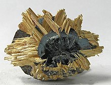
Rutile epitaxial on hematite nearly 6 cm long. Bahia, Brazil

In mineralogy, epitaxy is the overgrowth of one mineral on another in an orderly way, such that certain crystal directions of the two minerals are aligned. This occurs when some planes in the lattices of the overgrowth and the substrate have similar spacings between atoms.

If the crystals of both minerals are well formed so that the directions of the crystallographic axes are clear then the epitaxic relationship can be deduced just by a visual inspection.

Sometimes many separate crystals form the overgrowth on a single substrate, and then if there is epitaxy all the overgrowth crystals will have a similar orientation. The reverse, however, is not necessarily true. If the overgrowth crystals have a similar orientation there is probably an epitaxic relationship, but it is not certain.

Some authors consider that overgrowths of a second generation of the same mineral species should also be considered as epitaxy, and this is common terminology for semiconductor scientists who induce epitaxic growth of a film with a different doping level on a semiconductor substrate of the same material. For naturally produced minerals, however, the International Mineralogical Association (IMA) definition requires that the two minerals be of different species.

Another man-made application of epitaxy is the making of artificial snow using silver iodide, which is possible because hexagonal silver iodide and ice have similar cell dimensions.

Isomorphic minerals

Minerals that have the same structure (isomorphic minerals) may have epitaxic relations. An example is albite NaAlSi
3
O
8
on microcline KAlSi
3
O
8
. Both these minerals are triclinic, with space group 1, and with similar unit cell parameters, a = 8.16 Å, b = 12.87 Å, c = 7.11 Å, α = 93.45°, β = 116.4°, γ = 90.28° for albite and a = 8.5784 Å, b = 12.96 Å, c = 7.2112 Å, α = 90.3°, β = 116.05°, γ = 89° for microcline. 

Polymorphic minerals

text
Rutile on hematite, from Novo Horizonte, Bahia, Northeast Region, Brazil
text
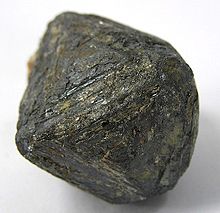
Hematite pseudomorph after magnetite, with terraced epitaxial faces. La Rioja, Argentina
Minerals that have the same composition but different structures (polymorphic minerals) may also have epitaxic relations. Examples are pyrite and marcasite, both FeS2, and sphalerite and wurtzite, both ZnS.

Rutile on hematite

Some pairs of minerals that are not related structurally or compositionally may also exhibit epitaxy. A common example is rutile TiO2 on hematite Template:Fe. Rutile is tetragonal and hematite is trigonal, but there are directions of similar spacing between the atoms in the (100) plane of rutile (perpendicular to the a axis) and the (001) plane of hematite (perpendicular to the c axis). In epitaxy these directions tend to line up with each other, resulting in the axis of the rutile overgrowth being parallel to the c axis of hematite, and the c axis of rutile being parallel to one of the axes of hematite.

Hematite on magnetite

Another example is hematite Fe3+
2
O
3
on magnetite Fe2+Fe3+
2
O
4
. The magnetite structure is based on close-packed oxygen anions stacked in an ABC-ABC sequence. In this packing the close-packed layers are parallel to (111) (a plane that symmetrically "cuts off" a corner of a cube). The hematite structure is based on close-packed oxygen anions stacked in an AB-AB sequence, which results in a crystal with hexagonal symmetry.

If the cations were small enough to fit into a truly close-packed structure of oxygen anions then the spacing between the nearest neighbour oxygen sites would be the same for both species. The radius of the oxygen ion, however, is only 1.36 Å and the Fe cations are big enough to cause some variations. The Fe radii vary from 0.49 Å to 0.92 Å, depending on the charge (2+ or 3+) and the coordination number (4 or 8). Nevertheless, the O spacings are similar for the two minerals hence hematite can readily grow on the (111) faces of magnetite, with hematite (001) parallel to magnetite (111).

Semiconductor device fabrication

 
NASA's Glenn Research Center clean room
 
Semiconductor device fabrication is the process used to manufacture semiconductor devices, typically the metal-oxide-semiconductor (MOS) devices used in the integrated circuit (IC) chips that are present in everyday electrical and electronic devices. It is a multiple-step sequence of photolithographic and chemical processing steps (such as surface passivation, thermal oxidation, planar diffusion and junction isolation) during which electronic circuits are gradually created on a wafer made of pure semiconducting material. Silicon is almost always used, but various compound semiconductors are used for specialized applications.

The entire manufacturing process, from start to packaged chips ready for shipment, takes six to eight weeks and is performed in highly specialized facilities referred to as foundries or fabs. In more advanced semiconductor devices, such as modern 14/10/7 nm nodes, fabrication can take up to 15 weeks (about 4 months) with 11–13 weeks (3 to 4 months) being the industry average. Production in advanced fabrication facilities is completely automated, and carried out in a hermetically sealed, nitrogen environment to improve yield (the proportion of microchips in a wafer that function correctly) with FOUPs and automated material handling systems taking care of the transport of wafers from machine to machine. All machinery as well as FOUPs contain an internal nitrogen atmosphere. The air inside the machinery and the FOUPs is usually kept cleaner than the surrounding air in the cleanroom. This internal atmosphere is known as a mini environment. Fab's need for large amounts of liquid nitrogen arises from the need to mantain the nitrogen atmosphere inside produciton machnery and FOUPs, which are constantly purged with nitrogen.

By industry standard, each generation of the semiconductor manufacturing process, also known as technology node, is designated by the process’s minimum feature size. Technology nodes, also known as "process technologies" or simply "nodes", are typically indicated by the size in nanometers (or historically micrometers) of the process's transistor gate length.

History


20th century

The first MOSFET (metal-oxide-silicon field-effect transistor) semiconductor devices were fabricated by Egyptian engineer Mohamed M. Atalla and Korean engineer Dawon Kahng at Bell Labs between 1959 and 1960. There were originally two types of MOSFET technology, PMOS (p-type MOS) and NMOS (n-type MOS). Both types were developed by Atalla and Kahng when they originally invented the MOSFET, fabricating both PMOS and NMOS devices at 20 µm and 10 µm scales.

An improved type of MOSFET technology, CMOS, was developed by Chih-Tang Sah and Frank Wanlass at Fairchild Semiconductor in 1963. CMOS was commercialised by RCA in the late 1960s. RCA commercially used CMOS for its 4000-series integrated circuits in 1968, starting with a 20 µm process before gradually scaling to a 10 µm process over the next several years.

Semiconductor device manufacturing has since spread from Texas and California in the 1960s to the rest of the world, including Asia, Europe, and the Middle East

21st century

The semiconductor industry is a global business today. The leading semiconductor manufacturers typically have facilities all over the world. Samsung Electronics, the world's largest manufacturer of semiconductors, has facilities in South Korea and the US. Intel, the second largest manufacturer, has facilities in Europe and Asia as well as the US. TSMC, the world's largest pure play foundry, has facilities in Taiwan, China, Singapore, and the US. Qualcomm and Broadcom are among the biggest fabless semiconductor companies, outsourcing their production to companies like TSMC. They also have facilities spread in different countries. 

Since 2009, "node" has become a commercial name for marketing purposes that indicates new generations of process technologies, without any relation to gate length, metal pitch or gate pitch. For example, GlobalFoundries' 7 nm process is similar to Intel's 10 nm process, thus the conventional notion of a process node has become blurred. Additionally, TSMC and Samsung's 10 nm processes are only slightly denser than Intel's 14 nm in transistor density. They are actually much closer to Intel's 14 nm process than they are to Intel's 10 nm process (e.g. Samsung's 10 nm processes' fin pitch is the exact same as that of Intel's 14 nm process: 42 nm).

As of 2019, 14 nanometer and 10 nanometer chips are in mass production by Intel, UMC, TSMC, Samsung, Micron, SK Hynix, Toshiba Memory and GlobalFoundries, with 7 nanometer process chips in mass production by TSMC and Samsung, although their 7 nanometer node definition is similar to Intel's 10 nanometer process. The 5 nanometer process began being produced by Samsung in 2018. As of 2019, the node with the highest transistor density is TSMC's 5 nanometer N5 node, with a density of 171.3 million transistors per square millimeter. In 2019, Samsung and TSMC announced plans to produce 3 nanometer nodes. GlobalFoundries has decided to stop the development of new nodes beyond 12 nanometers in order to save resources, as it has determined that setting up a new fab to handle sub-12nm orders would be beyond the company's financial abilities. As of 2019, Samsung is the industry leader in advanced semiconductor scaling, followed by TSMC and then Intel.

List of steps

This is a list of processing techniques that are employed numerous times throughout the construction of a modern electronic device; this list does not necessarily imply a specific order. Equipment for carrying out these processes is made by a handful of companies. All equipment needs to be tested before a semiconductor fabrication plant is started. 
Progress of miniaturisation, and comparison of sizes of semiconductor manufacturing process nodes with some microscopic objects and visible light wavelengths.

Prevention of contamination and defects

When feature widths were far greater than about 10 micrometres, semiconductor purity was not as big of an issue as it is today in device manufacturing. As devices became more integrated, cleanrooms must become even cleaner. Today, fabrication plants are pressurized with filtered air to remove even the smallest particles, which could come to rest on the wafers and contribute to defects. The workers in a semiconductor fabrication facility are required to wear cleanroom suits to protect the devices from human contamination. To prevent oxidation and to increase yield, FOUPs and semiconductor capital equipment may have a pure nitrogen environment with ISO class 1 levels of dust. 

Wafers

A typical wafer is made out of extremely pure silicon that is grown into mono-crystalline cylindrical ingots (boules) up to 300 mm (slightly less than 12 inches) in diameter using the Czochralski process. These ingots are then sliced into wafers about 0.75 mm thick and polished to obtain a very regular and flat surface. 

Processing

In semiconductor device fabrication, the various processing steps fall into four general categories: deposition, removal, patterning, and modification of electrical properties.
Modern chips have up to eleven metal levels produced in over 300 sequenced processing steps.

Front-end-of-line (FEOL) processing

FEOL processing refers to the formation of the transistors directly in the silicon. The raw wafer is engineered by the growth of an ultrapure, virtually defect-free silicon layer through epitaxy. In the most advanced logic devices, prior to the silicon epitaxy step, tricks are performed to improve the performance of the transistors to be built. One method involves introducing a straining step wherein a silicon variant such as silicon-germanium (SiGe) is deposited. Once the epitaxial silicon is deposited, the crystal lattice becomes stretched somewhat, resulting in improved electronic mobility. Another method, called silicon on insulator technology involves the insertion of an insulating layer between the raw silicon wafer and the thin layer of subsequent silicon epitaxy. This method results in the creation of transistors with reduced parasitic effects

Gate oxide and implants

Front-end surface engineering is followed by growth of the gate dielectric (traditionally silicon dioxide), patterning of the gate, patterning of the source and drain regions, and subsequent implantation or diffusion of dopants to obtain the desired complementary electrical properties. In dynamic random-access memory (DRAM) devices, storage capacitors are also fabricated at this time, typically stacked above the access transistor (the now defunct DRAM manufacturer Qimonda implemented these capacitors with trenches etched deep into the silicon surface).

Back-end-of-line (BEOL) processing


Metal layers

Once the various semiconductor devices have been created, they must be interconnected to form the desired electrical circuits. This occurs in a series of wafer processing steps collectively referred to as BEOL (not to be confused with back end of chip fabrication, which refers to the packaging and testing stages). BEOL processing involves creating metal interconnecting wires that are isolated by dielectric layers. The insulating material has traditionally been a form of SiO2 or a silicate glass, but recently new low dielectric constant materials are being used (such as silicon oxycarbide), typically providing dielectric constants around 2.7 (compared to 3.82 for SiO2), although materials with constants as low as 2.2 are being offered to chipmakers.

Interconnect

Synthetic detail of a standard cell through four layers of planarized copper interconnect, down to the polysilicon (pink), wells (greyish) and substrate (green).
 
Historically, the metal wires have been composed of aluminum. In this approach to wiring (often called subtractive aluminum), blanket films of aluminum are deposited first, patterned, and then etched, leaving isolated wires. Dielectric material is then deposited over the exposed wires. The various metal layers are interconnected by etching holes (called "vias") in the insulating material and then depositing tungsten in them with a CVD technique; this approach is still used in the fabrication of many memory chips such as dynamic random-access memory (DRAM), because the number of interconnect levels is small (currently no more than four). 

More recently, as the number of interconnect levels for logic has substantially increased due to the large number of transistors that are now interconnected in a modern microprocessor, the timing delay in the wiring has become so significant as to prompt a change in wiring material (from aluminum to copper interconnect layer) and a change in dielectric material (from silicon dioxides to newer low-K insulators). This performance enhancement also comes at a reduced cost via damascene processing, which eliminates processing steps. As the number of interconnect levels increases, planarization of the previous layers is required to ensure a flat surface prior to subsequent lithography. Without it, the levels would become increasingly crooked, extending outside the depth of focus of available lithography, and thus interfering with the ability to pattern. CMP (chemical-mechanical planarization) is the primary processing method to achieve such planarization, although dry etch back is still sometimes employed when the number of interconnect levels is no more than three.

Wafer test

The highly serialized nature of wafer processing has increased the demand for metrology in between the various processing steps. For example, thin film metrology based on ellipsometry or reflectometry is used to tightly control the thickness of gate oxide, as well as the thickness, refractive index and extinction coefficient of photoresist and other coatings. Wafer test metrology equipment is used to verify that the wafers haven't been damaged by previous processing steps up until testing; if too many dies on one wafer have failed, the entire wafer is scrapped to avoid the costs of further processing. Virtual metrology has been used to predict wafer properties based on statistical methods without performing the physical measurement itself.

Device test

Once the front-end process has been completed, the semiconductor devices are subjected to a variety of electrical tests to determine if they function properly. The proportion of devices on the wafer found to perform properly is referred to as the yield. Manufacturers are typically secretive about their yields, but it can be as low as 30%. Process variation is one among many reasons for low yield.

The fab tests the chips on the wafer with an electronic tester that presses tiny probes against the chip. The machine marks each bad chip with a drop of dye. Currently, electronic dye marking is possible if wafer test data is logged into a central computer database and chips are "binned" (i.e. sorted into virtual bins) according to the predetermined test limits. The resulting binning data can be graphed, or logged, on a wafer map to trace manufacturing defects and mark bad chips. This map can also be used during wafer assembly and packaging.

Chips are also tested again after packaging, as the bond wires may be missing, or analog performance may be altered by the package. This is referred to as the "final test". 

Usually, the fab charges for testing time, with prices in the order of cents per second. Testing times vary from a few milliseconds to a couple of seconds, and the test software is optimized for reduced testing time. Multiple chip (multi-site) testing is also possible, because many testers have the resources to perform most or all of the tests in parallel.

Chips are often designed with "testability features" such as scan chains or a "built-in self-test" to speed testing, and reduce testing costs. In certain designs that use specialized analog fab processes, wafers are also laser-trimmed during testing, in order to achieve tightly-distributed resistance values as specified by the design.

Good designs try to test and statistically manage corners (extremes of silicon behavior caused by a high operating temperature combined with the extremes of fab processing steps). Most designs cope with at least 64 corners. 

Die preparation

Once tested, a wafer is typically reduced in thickness in a process also known as "backlap", "backfinish" or "wafer thinning" before the wafer is scored and then broken into individual dice, a process known as wafer dicing. Only the good, unmarked chips are packaged. 

Packaging

Plastic or ceramic packaging involves mounting the die, connecting the die pads to the pins on the package, and sealing the die. Tiny bondwires are used to connect the pads to the pins. Originally, wires were attached by hand, but now specialized machines perform the task. Traditionally, these wires have been composed of gold, leading to a lead frame (pronounced "leed frame") of solder-plated copper; lead is poisonous, so lead-free "lead frames" are now mandated by RoHS.

Chip scale package (CSP) is another packaging technology. A plastic dual in-line package, like most packages, is many times larger than the actual die hidden inside, whereas CSP chips are nearly the size of the die; a CSP can be constructed for each die before the wafer is diced.

The packaged chips are retested to ensure that they were not damaged during packaging and that the die-to-pin interconnect operation was performed correctly. A laser then etches the chip's name and numbers on the package. 

Hazardous materials

Many toxic materials are used in the fabrication process. These include:
It is vital that workers should not be directly exposed to these dangerous substances. The high degree of automation common in the IC fabrication industry helps to reduce the risks of exposure. Most fabrication facilities employ exhaust management systems, such as wet scrubbers, combustors, heated absorber cartridges, etc., to control the risk to workers and to the environment. 


Inequality (mathematics)

From Wikipedia, the free encyclopedia https://en.wikipedia.org/wiki/Inequality...