Search This Blog

Saturday, January 5, 2019

Transparent conducting film

From Wikipedia, the free encyclopedia

Figure 1. Cross-section of thin film polycrystalline solar cell. The transparent conducting coating contacts the n-type semiconductor to draw current.
 
Transparent conducting films (TCFs) are thin films of optically transparent and electrically conductive material. They are an important component in a number of electronic devices including liquid-crystal displays, OLEDs, touchscreens and photovoltaics. While indium tin oxide (ITO) is the most widely used, alternatives include wider-spectrum transparent conductive oxides (TCOs), conductive polymers, metal grids and random metallic networks, carbon nanotubes (CNT), graphene, nanowire meshes and ultra thin metal films.

TCFs for photovoltaic applications have been fabricated from both inorganic and organic materials. Inorganic films typically are made up of a layer of transparent conducting oxide (TCO), most commonly indium tin oxide (ITO), fluorine doped tin oxide (FTO)  or doped zinc oxide. Organic films are being developed using carbon nanotube networks and graphene, which can be fabricated to be highly transparent to infrared light, along with networks of polymers such as poly(3,4-ethylenedioxythiophene) and its derivatives. 

Transparent conducting films are typically used as electrodes when a situation calls for low resistance electrical contacts without blocking light (e.g. LEDs, photovoltaics). Transparent materials possess wide bandgaps whose energy value is greater than those of visible light. As such, photons with energies below the bandgap value are not absorbed by these materials and visible light passes through. Some applications, such as solar cells, often require a wider range of transparency beyond visible light to make efficient use of the full solar spectrum.

Transparent conducting oxides

This solar cell, made of monocrystalline silicon, has no transparent conducting film. Instead, it uses a "grid contact": a network of very thin metal wires.

Overview

Transparent conductive oxides (TCO) are doped metal oxides used in optoelectronic devices such as flat panel displays and photovoltaics (including inorganic devices, organic devices, and dye-sensitized solar cell). Most of these films are fabricated with polycrystalline or amorphous microstructures. Typically, these applications use electrode materials that have greater than 80% transmittance of incident light as well as electrical conductivities higher than 103 S/cm for efficient carrier transport. In general, TCOs for use as thin-film electrodes in solar cells should have a minimum carrier concentration on the order of 1020 cm−3 for low resistivity and a bandgap greater than 3.2 eV to avoid absorption of light over most of the solar spectra. Mobility in these films is typically limited by ionized impurity scattering due to the large amount of ionized dopant atoms and is on the order of 40 cm2/(V·s) for the best performing TCOs. Current transparent conducting oxides used in industry are primarily n-type conductors, meaning their primary conduction is as donors of electrons. This is because electron mobilities are typically higher than hole mobilities, making it difficult to find shallow acceptors in wide band gap oxides to create a large hole population. Suitable p-type transparent conducting oxides are still being researched, though the best of them are still orders of magnitude behind n-type TCOs. The lower carriers' concentration of TCOs with respect to metals shift their plasma resonance in the NIR and SWIR range.

To date, the industry standard in TCOs is ITO, or indium tin oxide. This material boasts a low resistivity of ~10−4 Ω·cm and a transmittance of greater than 80%. ITO has the drawback of being expensive. Indium, the film’s primary metal, is rare (6000 metric tons worldwide in 2006), and its price fluctuates due to market demand (over $800 per kg in 2006). For this reason, doped binary compounds such as aluminum-doped zinc oxide (AZO) and indium-doped cadmium oxide have been proposed as alternative materials. AZO is composed of aluminum and zinc, two common and inexpensive materials, while indium-doped cadmium oxide only uses indium in low concentrations. Other novel transparent conducting oxides include barium stannate and the correlated metal oxides strontium vanadate and calcium vanadate. 

Binary compounds of metal oxides without any intentional impurity doping have also been developed for use as TCOs. These systems are typically n-type with a carrier concentration on the order of 1020 cm−3, provided by interstitial metal ions and oxygen vacancies which both act as donors. However, these simple TCOs have not found practical use due to the high dependence of their electrical properties on temperature and oxygen partial pressure.

In current research, labs are looking to optimize the electrical and optical characteristics of certain TCOs. Researchers deposit TCO onto the sample by using a sputtering machine. The targets have been changed and researchers are looking at materials such as IZO (Indium Zinc Oxide), ITO (Indium Tin Oxide) and AZO (Aluminum Zinc Oxide), and they are optimizing these materials by changing parameters within the sputtering deposition machine. When researchers vary parameters such as concentration of the gases within the sputtering, the pressure within the sputtering machine, power of the sputtering, and pressure, they are able to achieve different carrier concentrations and sheet resistivities within the machine. Carrier concentrations affect the short circuit current of the sample, and a change in sheet resistivity affects the fill factor of the sample. Researchers have varied parameters enough and found combinations that will optimize the short circuit current as well as the fill factor for TCOs such as indium tin oxide.

Fabrication

Doped metal oxides for use as transparent conducting layers in photovoltaic devices are typically grown on a glass substrate. This glass substrate, apart from providing a support that the oxide can grow on, has the additional benefit of blocking most infrared wavelengths greater than 2 µm for most silicates, and converting it to heat in the glass layer. This in turn helps maintain a low temperature of the active region of the solar cell, which degrades in performance as it heats up. TCO films can be deposited on a substrate through various deposition methods, including metal organic chemical vapor deposition (MOCVD), metal organic molecular beam deposition (MOMBD), solution deposition, spray pyrolysis, ultrasonic nozzle sprayed graphene oxide and air sprayed Ag Nanowire and pulsed laser deposition (PLD), however conventional fabrication techniques typically involve magnetron sputtering of the film. The sputtering process is very inefficient, with only 30% of planar target material available for deposition on the substrate. Cylindrical targets offer closer to 80% utilization. In the case of ITO recycling of unused target material is required for economic production. For AZO or ZnAl sputtering target material is sufficiently inexpensive that recovery of materials use is of no concern. There is some concern that there is a physical limit to the available indium for ITO. Growth typically is performed in a reducing environment to compensating acceptor defects within the film (e.g. metal vacancies), which degrade the carrier concentration (if n-type).

For AZO thin film deposition, the coating method of reactive magnetron sputtering is a very economical and practical way of mass production. In this method, a Zn-Al metal target is sputtered in an oxygen atmosphere such that metal ions oxidize when they reach the substrates surface. By using a metal target instead of an oxide target, direct current magnetron sputtering may be used which enable much faster deposition rates.

Theory

Charge carriers in these n-type oxides arise from three fundamental sources: interstitial metal ion impurities, oxygen vacancies, and doping ions. The first two sources always act as electron donors; indeed, some TCOs are fabricated solely using these two intrinsic sources as carrier generators. When an oxygen vacancy is present in the lattice it acts as a doubly charged electron donor. In ITO, for example, each oxygen vacancy causes the neighboring In3+ ion 5s orbitals to be stabilized from the 5s conduction band by the missing bonds to the oxygen ion, while two electrons are trapped at the site due to charge neutrality effects. This stabilization of the 5s orbitals causes a formation of a donor level for the oxygen ion, determined to be 0.03 eV below the conduction band. Thus these defects act as shallow donors to the bulk crystal. Common notation for this doping is Kröger–Vink notation and is written as:
Here “O” in the subscripts indicates that both the initially bonded oxygen and the vacancy that is produced lie on an oxygen lattice site, while the superscripts on the oxygen and vacancy indicate charge. Thus to enhance their electrical properties, ITO films and other transparent conducting oxides are grown in reducing environments, which encourage oxygen vacancy formation.

Dopant ionization within the oxide occurs in the same way as in other semiconductor crystals. Shallow donors near the conduction band (n-type) allow electrons to be thermally excited into the conduction band, while acceptors near the valence band (p-type) allow electrons to jump from the valence band to the acceptor level, populating the valence band with holes. It is important to note that carrier scattering in these oxides arises primarily from ionized impurity scattering at high dopant levels (>1 at%). Charged impurity ions and point defects have scattering cross-sections that are much greater than their neutral counterparts. Increasing the scattering decreases the mean-free path of the carriers in the oxide, which leads to low electron mobility and a high resistivity. These materials can be modeled reasonably well by the free electron model assuming a parabolic conduction band and doping levels above the Mott Criterion. This criterion states that an insulator such as an oxide can experience a composition-induced transition to a metallic state given a minimum doping concentration nc, determined by:
where aH* is the mean ground state Bohr radius. For ITO, this value requires a minimum doping concentration of roughly 1019 cm−3. Above this level, the conduction type in the material switches from semiconductor to metallic.

Transparent conducting polymers

Figure 2. Polymer photovoltaic cell using transparent conducting polymers.
 
Conductive polymers were reported in the mid the 20th century as derivatives of polyaniline. Research continued on such polymers in the 1960s and 70s and continued into the turn of the 21st century. Most conductive polymers are derivatives of polyacetylene, polyaniline, polypyrrole or polythiophenes. These polymers have conjugated double bonds which allow for conduction. By manipulating the band structure, polythiophenes have been modified to achieve a HOMO-LUMO separation (bandgap) that is large enough to make them transparent to visible light.

Applications

Transparent conductive polymers are used as electrodes on light emitting diodes and photovoltaic devices. They have conductivity below that of transparent conducting oxides but have low absorption of the visible spectrum allowing them to act as a transparent conductor on these devices. However, because transparent conductive polymers do absorb some of the visible spectrum and significant amounts of the mid to near IR, they lower the efficiency of photovoltaic devices.

The transparent conductive polymers can be made into flexible films making them desirable despite their lower conductivity. This makes them useful in the development of flexible electronics where traditional transparent conductors will fail.

Poly(3,4-ethylenedioxythiophene) (PEDOT)

Poly(3,4-ethylenedioxythiophene) (PEDOT) has conductivity of up to around 1,000 S/cm. Thin oxidized PEDOT films have approx. 10% or less absorption in the visible spectrum and excellent stability. However, PEDOT is insoluble in water making processing more difficult and costly.

The bandgap of PEDOT can be varied between 1.4 and 2.5 eV by varying the degree of π-overlap along the backbone. This can be done by adding substituents along the chain, which result in steric interactions preventing π-overlap. Substituents can also be electron-accepting or donating which will modify the electronic character and thus modify the bandgap. This allows for the formation of a wide bandgap conductor which is transparent to the visible spectrum.

PEDOT is prepared by mixing EDT monomer with an oxidizing agent such as FeCl3. The oxidizing agent acts as an initiator for polymerization. Research has shown that increasing the ratio of [FeCl3]/[monomer] decreases the solubility of the PEDOT. This is thought to be a result of increased crosslinking in the polymer making it more difficult to dissolve in a solvent.

Poly(3,4-ethylenedioxythiophene) PEDOT: poly(styrene sulfonate) PSS

Doping PEDOT with poly(styrene sulfonate) can improve the properties over the unmodified PEDOT. This PEDOT:PSS compound has become the industry leader in transparent conductive polymers. PEDOT:PSS is water-soluble, making processing easier. PEDOT:PSS has a conductivity ranging from 400 to 600 S/cm while still transmitting ~80% of visible light. Treatment in air at 100 °C for over 1000 hours will result in a minimal change in conductivity. Recently, it was reported that the conductivity of PEDOT:PSS can be improved to be more than 4600 S/cm.

PEDOT:PSS is prepared by polymerizing EDT monomer in an aqueous solution of PSS using Na2S2O8 as the oxidizing agent. This aqueous solution is then spin coated and dried to make a film.

Poly(4,4-dioctyl cyclopentadithiophene)

Poly(4,4-dioctyl cyclopentadithiophene) can be doped with iodine or 2,3-dichloro-5,6-dicyano-1,4-benzoquinone (DDQ) to form a transparent conductor. The doped polymer has low absorption of the visible spectrum with an absorption band centered around 1050 nm. When doped with iodine, a conductivity of 0.35 S/cm can be achieved. However, the iodine has a tendency to diffuse out in air, making the iodine-doped poly(4,4-dioctyl cyclopentadithiophene) unstable.

DDQ itself has a conductivity of 1.1 S/cm. However, DDQ-doped poly(4,4-dioctyl cyclopentadithiophene) also tends to decrease its conductivity in air. DDQ-doped polymer has better stability than the iodine-doped polymer, but the stability is still below that of PEDOT. In summary, poly(4,4-dioctyl cyclopentadithiophene) has inferior properties relative to PEDOT and PEDOT:PSS, which need to be improved for realistic applications.

Poly(4,4-dioctyl cyclopentadithiophene) is solution polymerized by combining monomer with iron(III) chloride. Once the polymerization is complete the doping is done by exposing the polymer to iodine vapor or DDQ solution.

Carbon nanotubes

Advantages

Transparent conductors are fragile and tend to break down due to fatigue. The most commonly used TCO is Indium-Tin-Oxide (ITO) because of its good electrical properties and ease of fabrication. However, these thin films are usually fragile and such problems as lattice mismatch and stress-strain constraints lead to restrictions in possible uses for TCFs. ITO has been shown to degrade with time when subject to mechanical stresses. Recent increases in cost are also forcing many to look to carbon nanotube films as a potential alternative. 

Carbon nanotubes (CNTs) have attracted much attention because of their materials properties, including a high elastic modulus (~1–2 TPa), a high tensile strength (~13–53 GPa), and a high conductivity (metallic tubes can theoretically carry an electric current density of 4×10⁹ A/cm2, which is ~1000 times higher than for other metals such as copper). CNT thin films have been used as transparent electrodes in TCFs because of these good electronic properties.

Preparation of CNT thin films

Figure 3. CNTs of various diameters separated within a centrifuge tube. Each distinct diameter results in a different color.
 
The preparation of CNT thin films for TCFs is composed of three steps: the CNT growth process, putting the CNTs in solution, and, finally, creation of the CNT thin film. Nanotubes can be grown using laser ablation, electric-arc discharge, or different forms of chemical vapor deposition (such as PECVD). However, nanotubes are grown en-masse, with nanotubes of different chiralities stuck together due to van der Waals attraction. Density gradient ultracentrifugation (DGU) has recently been used to get rid of this problem. Using DGU, transparent conductors were constructed using only metallic tubes. Because DGU allows for separation by density, tubes with similar optical properties (due to similar diameters) were selected and used to make CNT conductive films of different colors.

In order to separate the grown tubes, the CNTs are mixed with surfactant and water and sonicated until satisfactory separation occurs. This solution is then sprayed onto the desired substrate in order to create a CNT thin film. The film is then rinsed in water in order to get rid of excess surfactant.

One method of spray deposition used for CNT film creation is an ultrasonic nozzle to atomize CNTs in solution to form PEDOT layers.

By optimizing spray parameters, including surfactant, drop size (dictated by the ultrasonic nozzle frequency) and solution flow rate, sheet resistance characteristics can be tuned. Due to the ultrasonic vibration of the nozzle itself, this method also provides an additional level of sonification during the spray process for added separation of agglomerated CNTs.

Comparing CNTs to TCOs

CNTs can also be used in addition to transparent conducting oxides (TCOs) in thin-film photovoltaic devices. Two TCOs which are often used are ZnO/Al and In2O3/Sn indium tin oxide (ITO). PV devices made with these TCOs attained energy-conversion efficiencies of 19.5% in CuIn1−xGaxSe2-based (CIGS) solar cells and 16.5% in CdTe-based solar cells. These photovoltaic devices had much higher efficiencies compared to the devices made with CNT thin films: Britz et al. report an efficiency of 8%, with an open circuit voltage (Voc) of 0.676 V, a short circuit flux (Jsc) of 23.9 mA/cm2, and a fill factor of 45.48%. However, CNT thin films show many advantages over other transparent electrodes in the IR range. CNT thin films were reported to have a transmittance of over 90% in this range (400 nm – 22 µm). This paves the way for new applications, indicating that CNT thin films can be used as heat dissipaters in solar cells because of this high transmittance. 

As stated previously, nanotube chirality is important in helping determine its potential aid to these devices. Before mass production can occur, more research is needed in exploring the significance of tube diameter and chirality for transparent conducting films in photovoltaic applications. It is expected that the conductivity of the SWNT thin films will increase with an increase in CNT length and purity. As stated previously, the CNT films are made using randomly oriented bundles of CNTs. Ordering these tubes should also increase conductivity, as it will minimise scattering losses and improve contact between the nanotubes.

Conducting nanowire networks and metal mesh as flexible transparent electrodes

Figure 4. Schematic of metal network based Transparent Conducting Electrodes. Electrical transport is through the percolating metal network, while optical transmittance is through the voids.
 
Randomly conducting networks of wires or metal meshes obtained from templates are new generation transparent electrodes. In these electrodes, nanowire or metal mesh network is charge collector, while the voids between them are transparent to light. These are obtained from the deposition of silver or copper nanowires, or by depositing metals in templates such as hierarchical patterns of random cracks, leaves venation and grain boundaries etc. These metal networks can be made on flexible substrates and can act as flexible transparent electrodes. For better performance of these conducting network based electrodes, optimized density of nanowires has to be used as excess density, leads to shadowing losses in solar cells, while the lower density of the wires, leads to higher sheet resistance and more recombination losses of charge carriers generated in solar cells.

This Bill Gates-Backed Company Is Developing a Possibly World-Changing Nuclear Reactor

By Peter Kotecki, Business Insider, December 01, 2018

Bill Gates sees nuclear energy as a potential solution to lowering carbon-dioxide emissions around the world, and he has spent the past decade funding new ways to produce the energy in a safe, affordable way.

About 10 years ago, Gates cofounded a company called TerraPower to build new kinds of nuclear reactors.

TerraPower is developing a line of reactors that use a molten-chloride coolant, drawing on a decades-old, but still unused, invention to lower costs and reduce waste.

The most common reactors use light (or regular) water as a coolant.

Following a US Department of Energy investment worth US$40 million and a partnership with energy provider Southern Company, TerraPower plans on opening a new laboratory next year.

Gates' company wants to develop a molten-chloride prototype by 2030, and the laboratory will be used to test reactor materials in the meantime.

John Gilleland, the company's chief technology officer, told Business Insider that molten chloride designs are the "ultimate green reactor".

"It not only would allow you to produce electricity without carbon emissions, but by shipping the heat directly to some process in an industrial facility, you can provide the necessary heat to cause reactions to occur in industrial processing, or whatever you want to use it for, without carbon emissions," Gilleland said.

How a molten-salt reactor works

Nuclear energy grew into prominence after 20th-century scientists figured out how to harness the atom's power, but high costs and safety concerns over dangerous radioactive waste have deterred many countries from investing in it.

Scientists at the Massachusetts Institute of Technology Energy Initiative wrote that within the electricity sector, nuclear energy would be the least expensive solution to reducing greenhouse-gas emissions in the next few decades.

But nuclear energy accounts for only 11 percent of the world's electricity, according to the World Nuclear Association.

Nuclear energy is produced when radioactive fuel is put into a reactor to trigger fission – a process in which the nucleus of an atom splits within a reactor core.

In light-water reactors, solid fuel sits within cladding, or corrosion-resistant metal that prevents radioactive pieces from contaminating the coolant. The water around the cladding helps turn a reaction's heat into steam for turbines, which generate electricity.

TerraPower's liquid-chloride design, however, puts uranium fuel and the coolant in the same molten salt, Gilleland said.

Fission can heat the salts directly as the mixture flows through the reactor core, and the mixture then goes through heat exchangers to generate heat or electricity, he said.

Light-water reactors can't sustain reactions at very high temperatures because the coolant evaporates. With molten chloride, though, TerraPower could operate reactors at much higher temperatures than before.

In addition to generating electricity, nuclear technology could be used in high-temperature processes like fertiliser production and oil refining.

The materials inside light-water reactors degrade quickly and need to be replaced roughly every 18 months, as it becomes more difficult to sustain fission with older fuel.

Molten-chloride reactors, meanwhile, produce little residual waste and could theoretically run for years without the need to add fuel or get rid of waste.

TerraPower's design is also less likely to be used in nuclear-weapon production because its radioactive fuel is not isolated.

TerraPower's new reactor was inspired by a 1960s experiment

Though TerraPower began working on its newest line of reactors just a few years ago, the design is based on Cold War-era molten-salt technology. (TerraPower has also spent the past decade developing a travelling-wave reactor, another advanced design.)

Researchers at the Oak Ridge National Laboratory in Tennessee developed a molten-salt reactor in the 1960s, but funding came to a halt several years later as scientists raised concerns about corrosion and safety problems associated with the reactor.

Now, with government funding and the support of billionaires like Gates, these reactors have another shot at hitting the market.

TerraPower and Southern Company are working on their design with scientists from Oak Ridge National Laboratory, Idaho National Laboratory, the Electric Power Research Institute, and Vanderbilt University.

Several other startups are competing with Gates' company to commercialize similar molten-salt reactors.

In April, Florida-based company ThorCon received US$400,000 from the US Department of Energy for a joint research project with Argonne National Laboratory.

ThorCon aims to begin testing a molten-salt-fuelled fission reactor by 2023.

Department of Energy officials have also given US$2.1 million to Alabama-based Flibe Energy, which is using thorium instead of uranium.

The molten-salt reactor movement extends beyond the US. Terrestrial Energy, a Canadian company, wants to commercialize the design for its Integral Molten Salt Reactor by the late 2020s .

And in the UK, Moltex Energy is making a Stable Salt Reactor, which uses molten-salt fuel. Moltex plans on deploying its product at a nuclear-reactor site by 2030.

At the same time, some nuclear startups have struggled to make their designs commercially viable. MIT-affiliated Transatomic Power, for example, shut down in September after seven years of operation.

The company, founded just after the 2011 nuclear disaster in Japan's Fukushima Prefecture, had claimed its reactors would produce electricity 75 times more efficiently than light-water reactors.

In a blog post announcing the shutdown, Transatomic CEO Leslie Dewan acknowledged there had been errors in early analyses and said the company was unable to scale up fast enough.

Transatomic Power later open-sourced its intellectual property for other researchers to use.

Clean energy is in urgent demand, and Gates' startup is at least a decade away from a working prototype

Renewable energy use is growing too slowly to prevent dangerous climate change on its own.

If governments don't implement new policies that reduce carbon-dioxide emissions, the bulk of the world's energy will still come from fossil fuels, according to the International Energy Agency's 2018 World Energy Outlook.

Solar, wind, and nuclear-energy systems are not keeping up with global energy demands, the report said.

About 25 percent of the world's electricity comes from renewable energy sources, according to the World Energy Outlook.

The International Energy Agency predicts that the share will rise to 40 percent by 2040, and nuclear energy can prove to be a vital factor in any changes.

For Southern Company and TerraPower, the companies' ambitious plan could produce a new reactor well before 2040.

The partners are developing a prototype with the capacity to produce up to 1,100 megawatts of electricity – enough to power about 825,000 homes, according to the California Energy Commission.

TerraPower's US$20 million laboratory, set to open in the state of Washington next year, will help researchers ensure the reactor is safe to run.

Gilleland said TerraPower will run tests with depleted uranium, which is not used in fission, to determine which materials can hold molten salt without being damaged by corrosion.

Gates, who still serves as TerraPower's chairman, has emphasised that fewer people die in nuclear-plant disasters than in coal-mine or natural-gas accidents.

During a 2010 speech at MIT, he also praised nuclear energy for its potential to benefit countries where solar and wind energy are scarce.

"It is infinite. You can filter out of the sea very cheaply enough uranium to run this thing for as long as the sun will shine," Gates said. "I love nuclear."
 
This article was originally published by Business Insider.

Transparency and translucency

From Wikipedia, the free encyclopedia

Dichroic filters are created using optically transparent materials.
 
In the field of optics, transparency (also called pellucidity or diaphaneity) is the physical property of allowing light to pass through the material without being scattered. On a macroscopic scale (one where the dimensions investigated are much larger than the wavelength of the photons in question), the photons can be said to follow Snell's Law. Translucency (also called translucence or translucidity) is a superset of transparency: it allows light to pass through, but does not necessarily (again, on the macroscopic scale) follow Snell's law; the photons can be scattered at either of the two interfaces, or internally, where there is a change in index of refraction. In other words, a translucent medium allows the transport of light while a transparent medium not only allows the transport of light but allows for image formation. Transparent materials appear clear, with the overall appearance of one color, or any combination leading up to a brilliant spectrum of every color. The opposite property of translucency is opacity

When light encounters a material, it can interact with it in several different ways. These interactions depend on the wavelength of the light and the nature of the material. Photons interact with an object by some combination of reflection, absorption and transmission. Some materials, such as plate glass and clean water, transmit much of the light that falls on them and reflect little of it; such materials are called optically transparent. Many liquids and aqueous solutions are highly transparent. Absence of structural defects (voids, cracks, etc.) and molecular structure of most liquids are mostly responsible for excellent optical transmission. 

Materials which do not transmit light are called opaque. Many such substances have a chemical composition which includes what are referred to as absorption centers. Many substances are selective in their absorption of white light frequencies. They absorb certain portions of the visible spectrum while reflecting others. The frequencies of the spectrum which are not absorbed are either reflected or transmitted for our physical observation. This is what gives rise to color. The attenuation of light of all frequencies and wavelengths is due to the combined mechanisms of absorption and scattering.

Transparency can provide almost perfect camouflage for animals able to achieve it. This is easier in dimly-lit or turbid seawater than in good illumination. Many marine animals such as jellyfish are highly transparent.

Comparisons of 1. opacity, 2. translucency, and 3. transparency; behind each panel is a star

Introduction

With regard to the absorption of light, primary material considerations include:
  • At the electronic level, absorption in the ultraviolet and visible (UV-Vis) portions of the spectrum depends on whether the electron orbitals are spaced (or "quantized") such that they can absorb a quantum of light (or photon) of a specific frequency, and does not violate selection rules. For example, in most glasses, electrons have no available energy levels above them in range of that associated with visible light, or if they do, they violate selection rules, meaning there is no appreciable absorption in pure (undoped) glasses, making them ideal transparent materials for windows in buildings.
  • At the atomic or molecular level, physical absorption in the infrared portion of the spectrum depends on the frequencies of atomic or molecular vibrations or chemical bonds, and on selection rules. Nitrogen and oxygen are not greenhouse gases because there is no absorption, but because there is no molecular dipole moment.
With regard to the scattering of light, the most critical factor is the length scale of any or all of these structural features relative to the wavelength of the light being scattered. Primary material considerations include:
  • Crystalline structure: whether or not the atoms or molecules exhibit the 'long-range order' evidenced in crystalline solids.
  • Glassy structure: scattering centers include fluctuations in density or composition.
  • Microstructure: scattering centers include internal surfaces such as grain boundaries, crystallographic defects and microscopic pores.
  • Organic materials: scattering centers include fiber and cell structures and boundaries.

Light scattering in solids

General mechanism of diffuse reflection

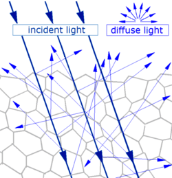
Diffuse reflection - Generally, when light strikes the surface of a (non-metallic and non-glassy) solid material, it bounces off in all directions due to multiple reflections by the microscopic irregularities inside the material (e.g., the grain boundaries of a polycrystalline material, or the cell or fiber boundaries of an organic material), and by its surface, if it is rough. Diffuse reflection is typically characterized by omni-directional reflection angles. Most of the objects visible to the naked eye are identified via diffuse reflection. Another term commonly used for this type of reflection is "light scattering". Light scattering from the surfaces of objects is our primary mechanism of physical observation.

Light scattering in liquids and solids depends on the wavelength of the light being scattered. Limits to spatial scales of visibility (using white light) therefore arise, depending on the frequency of the light wave and the physical dimension (or spatial scale) of the scattering center. Visible light has a wavelength scale on the order of a half a micrometer (one millionth of a meter). Scattering centers (or particles) as small as one micrometer have been observed directly in the light microscope (e.g., Brownian motion).

Transparent ceramics

Optical transparency in polycrystalline materials is limited by the amount of light which is scattered by their microstructural features. Light scattering depends on the wavelength of the light. Limits to spatial scales of visibility (using white light) therefore arise, depending on the frequency of the light wave and the physical dimension of the scattering center. For example, since visible light has a wavelength scale on the order of a micrometer, scattering centers will have dimensions on a similar spatial scale. Primary scattering centers in polycrystalline materials include microstructural defects such as pores and grain boundaries. In addition to pores, most of the interfaces in a typical metal or ceramic object are in the form of grain boundaries which separate tiny regions of crystalline order. When the size of the scattering center (or grain boundary) is reduced below the size of the wavelength of the light being scattered, the scattering no longer occurs to any significant extent. 

In the formation of polycrystalline materials (metals and ceramics) the size of the crystalline grains is determined largely by the size of the crystalline particles present in the raw material during formation (or pressing) of the object. Moreover, the size of the grain boundaries scales directly with particle size. Thus a reduction of the original particle size well below the wavelength of visible light (about 1/15 of the light wavelength or roughly 600/15 = 40 nanometers) eliminates much of light scattering, resulting in a translucent or even transparent material. 

Computer modeling of light transmission through translucent ceramic alumina has shown that microscopic pores trapped near grain boundaries act as primary scattering centers. The volume fraction of porosity had to be reduced below 1% for high-quality optical transmission (99.99 percent of theoretical density). This goal has been readily accomplished and amply demonstrated in laboratories and research facilities worldwide using the emerging chemical processing methods encompassed by the methods of sol-gel chemistry and nanotechnology.

Translucency of a material being used to highlight the structure of a photographic subject
 
Transparent ceramics have created interest in their applications for high energy lasers, transparent armor windows, nose cones for heat seeking missiles, radiation detectors for non-destructive testing, high energy physics, space exploration, security and medical imaging applications. Large laser elements made from transparent ceramics can be produced at a relatively low cost. These components are free of internal stress or intrinsic birefringence, and allow relatively large doping levels or optimized custom-designed doping profiles. This makes ceramic laser elements particularly important for high-energy lasers. 

The development of transparent panel products will have other potential advanced applications including high strength, impact-resistant materials that can be used for domestic windows and skylights. Perhaps more important is that walls and other applications will have improved overall strength, especially for high-shear conditions found in high seismic and wind exposures. If the expected improvements in mechanical properties bear out, the traditional limits seen on glazing areas in today's building codes could quickly become outdated if the window area actually contributes to the shear resistance of the wall. 

Currently available infrared transparent materials typically exhibit a trade-off between optical performance, mechanical strength and price. For example, sapphire (crystalline alumina) is very strong, but it is expensive and lacks full transparency throughout the 3–5 micrometer mid-infrared range. Yttria is fully transparent from 3–5 micrometers, but lacks sufficient strength, hardness, and thermal shock resistance for high-performance aerospace applications. Not surprisingly, a combination of these two materials in the form of the yttrium aluminium garnet (YAG) is one of the top performers in the field.

Absorption of light in solids

When light strikes an object, it usually has not just a single frequency (or wavelength) but many. Objects have a tendency to selectively absorb, reflect or transmit light of certain frequencies. That is, one object might reflect green light while absorbing all other frequencies of visible light. Another object might selectively transmit blue light while absorbing all other frequencies of visible light. The manner in which visible light interacts with an object is dependent upon the frequency of the light, the nature of the atoms in the object, and often the nature of the electrons in the atoms of the object.

Some materials allow much of the light that falls on them to be transmitted through the material without being reflected. Materials that allow the transmission of light waves through them are called optically transparent. Chemically pure (undoped) window glass and clean river or spring water are prime examples of this.

Materials which do not allow the transmission of any light wave frequencies are called opaque. Such substances may have a chemical composition which includes what are referred to as absorption centers. Most materials are composed of materials which are selective in their absorption of light frequencies. Thus they absorb only certain portions of the visible spectrum. The frequencies of the spectrum which are not absorbed are either reflected back or transmitted for our physical observation. In the visible portion of the spectrum, this is what gives rise to color.

Absorption centers are largely responsible for the appearance of specific wavelengths of visible light all around us. Moving from longer (0.7 micrometer) to shorter (0.4 micrometer) wavelengths: red, orange, yellow, green and blue (ROYGB) can all be identified by our senses in the appearance of color by the selective absorption of specific light wave frequencies (or wavelengths). Mechanisms of selective light wave absorption include:
  • Electronic: Transitions in electron energy levels within the atom (e.g., pigments). These transitions are typically in the ultraviolet (UV) and/or visible portions of the spectrum.
  • Vibrational: Resonance in atomic/molecular vibrational modes. These transitions are typically in the infrared portion of the spectrum.

UV-Vis: Electronic transitions

In electronic absorption, the frequency of the incoming light wave is at or near the energy levels of the electrons within the atoms which compose the substance. In this case, the electrons will absorb the energy of the light wave and increase their energy state, often moving outward from the nucleus of the atom into an outer shell or orbital

The atoms that bind together to make the molecules of any particular substance contain a number of electrons (given by the atomic number Z in the periodic chart). Recall that all light waves are electromagnetic in origin. Thus they are affected strongly when coming into contact with negatively charged electrons in matter. When photons (individual packets of light energy) come in contact with the valence electrons of atom, one of several things can and will occur:
  • A molecule absorbs the photon, some of the energy may be lost via luminescence, fluorescence and phosphorescence.
  • A molecule absorbs the photon which results in reflection or scattering.
  • A molecule cannot absorb the energy of the photon and the photon continues on its path. This results in transmission (provided no other absorption mechanisms are active).
Most of the time, it is a combination of the above that happens to the light that hits an object. The states in different materials vary in the range of energy that they can absorb. Most glasses, for example, block ultraviolet (UV) light. What happens is the electrons in the glass absorb the energy of the photons in the UV range while ignoring the weaker energy of photons in the visible light spectrum. But there are also existing special glass types, like special types of borosilicate glass or quartz that are UV-permeable and thus allow a high transmission of ultra violet light. 

Thus, when a material is illuminated, individual photons of light can make the valence electrons of an atom transition to a higher electronic energy level. The photon is destroyed in the process and the absorbed radiant energy is transformed to electric potential energy. Several things can happen then to the absorbed energy: it may be re-emitted by the electron as radiant energy (in this case the overall effect is in fact a scattering of light), dissipated to the rest of the material (i.e. transformed into heat), or the electron can be freed from the atom (as in the photoelectric and Compton effects).

Infrared: Bond stretching

Normal modes of vibration in a crystalline solid
 
The primary physical mechanism for storing mechanical energy of motion in condensed matter is through heat, or thermal energy. Thermal energy manifests itself as energy of motion. Thus, heat is motion at the atomic and molecular levels. The primary mode of motion in crystalline substances is vibration. Any given atom will vibrate around some mean or average position within a crystalline structure, surrounded by its nearest neighbors. This vibration in two dimensions is equivalent to the oscillation of a clock’s pendulum. It swings back and forth symmetrically about some mean or average (vertical) position. Atomic and molecular vibrational frequencies may average on the order of 1012 cycles per second (Terahertz radiation). 

When a light wave of a given frequency strikes a material with particles having the same or (resonant) vibrational frequencies, then those particles will absorb the energy of the light wave and transform it into thermal energy of vibrational motion. Since different atoms and molecules have different natural frequencies of vibration, they will selectively absorb different frequencies (or portions of the spectrum) of infrared light. Reflection and transmission of light waves occur because the frequencies of the light waves do not match the natural resonant frequencies of vibration of the objects. When infrared light of these frequencies strikes an object, the energy is reflected or transmitted. 

If the object is transparent, then the light waves are passed on to neighboring atoms through the bulk of the material and re-emitted on the opposite side of the object. Such frequencies of light waves are said to be transmitted.

Transparency in insulators

An object may be not transparent either because it reflects the incoming light or because it absorbs the incoming light. Almost all solids reflect a part and absorb a part of the incoming light. 

When light falls onto a block of metal, it encounters atoms that are tightly packed in a regular lattice and a "sea of electrons" moving randomly between the atoms. In metals, most of these are non-bonding electrons (or free electrons) as opposed to the bonding electrons typically found in covalently bonded or ionically bonded non-metallic (insulating) solids. In a metallic bond, any potential bonding electrons can easily be lost by the atoms in a crystalline structure. The effect of this delocalization is simply to exaggerate the effect of the "sea of electrons". As a result of these electrons, most of the incoming light in metals is reflected back, which is why we see a shiny metal surface. 

Most insulators (or dielectric materials) are held together by ionic bonds. Thus, these materials do not have free conduction electrons, and the bonding electrons reflect only a small fraction of the incident wave. The remaining frequencies (or wavelengths) are free to propagate (or be transmitted). This class of materials includes all ceramics and glasses

If a dielectric material does not include light-absorbent additive molecules (pigments, dyes, colorants), it is usually transparent to the spectrum of visible light. Color centers (or dye molecules, or "dopants") in a dielectric absorb a portion of the incoming light. The remaining frequencies (or wavelengths) are free to be reflected or transmitted. This is how colored glass is produced.

Most liquids and aqueous solutions are highly transparent. For example, water, cooking oil, rubbing alcohol, air, and natural gas are all clear. Absence of structural defects (voids, cracks, etc.) and molecular structure of most liquids are chiefly responsible for their excellent optical transmission. The ability of liquids to "heal" internal defects via viscous flow is one of the reasons why some fibrous materials (e.g., paper or fabric) increase their apparent transparency when wetted. The liquid fills up numerous voids making the material more structurally homogeneous.

Light scattering in an ideal defect-free crystalline (non-metallic) solid which provides no scattering centers for incoming light will be due primarily to any effects of anharmonicity within the ordered lattice. Light transmission will be highly directional due to the typical anisotropy of crystalline substances, which includes their symmetry group and Bravais lattice. For example, the seven different crystalline forms of quartz silica (silicon dioxide, SiO2) are all clear, transparent materials.

Optical waveguides

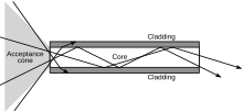
Propagation of light through a multi-mode optical fiber
 
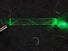
A laser beam bouncing down an acrylic rod, illustrating the total internal reflection of light in a multimode optical fiber
 
Optically transparent materials focus on the response of a material to incoming light waves of a range of wavelengths. Guided light wave transmission via frequency selective waveguides involves the emerging field of fiber optics and the ability of certain glassy compositions to act as a transmission medium for a range of frequencies simultaneously (multi-mode optical fiber) with little or no interference between competing wavelengths or frequencies. This resonant mode of energy and data transmission via electromagnetic (light) wave propagation is relatively lossless.

An optical fiber is a cylindrical dielectric waveguide that transmits light along its axis by the process of total internal reflection. The fiber consists of a core surrounded by a cladding layer. To confine the optical signal in the core, the refractive index of the core must be greater than that of the cladding. The refractive index is the parameter reflecting the speed of light in a material. (Refractive index is the ratio of the speed of light in vacuum to the speed of light in a given medium. The refractive index of vacuum is therefore 1.) The larger the refractive index, the more slowly light travels in that medium. Typical values for core and cladding of an optical fiber are 1.48 and 1.46, respectively.

When light traveling in a dense medium hits a boundary at a steep angle, the light will be completely reflected. This effect, called total internal reflection, is used in optical fibers to confine light in the core. Light travels along the fiber bouncing back and forth off of the boundary. Because the light must strike the boundary with an angle greater than the critical angle, only light that enters the fiber within a certain range of angles will be propagated. This range of angles is called the acceptance cone of the fiber. The size of this acceptance cone is a function of the refractive index difference between the fiber's core and cladding. Optical waveguides are used as components in integrated optical circuits (e.g. combined with lasers or light-emitting diodes, LEDs) or as the transmission medium in local and long haul optical communication systems.

Mechanisms of attenuation

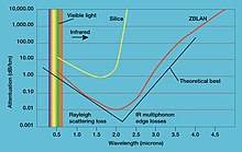
Light attenuation by ZBLAN and silica fibers
 
Attenuation in fiber optics, also known as transmission loss, is the reduction in intensity of the light beam (or signal) with respect to distance traveled through a transmission medium. Attenuation coefficients in fiber optics usually use units of dB/km through the medium due to the very high quality of transparency of modern optical transmission media. The medium is usually a fiber of silica glass that confines the incident light beam to the inside. Attenuation is an important factor limiting the transmission of a signal across large distances. In optical fibers the main attenuation source is scattering from molecular level irregularities (Rayleigh scattering) due to structural disorder and compositional fluctuations of the glass structure. This same phenomenon is seen as one of the limiting factors in the transparency of infrared missile domes. Further attenuation is caused by light absorbed by residual materials, such as metals or water ions, within the fiber core and inner cladding. Light leakage due to bending, splices, connectors, or other outside forces are other factors resulting in attenuation.

As camouflage

Many animals of the open sea, like this Aurelia labiata jellyfish, are largely transparent.

Many marine animals that float near the surface are highly transparent, giving them almost perfect camouflage. However, transparency is difficult for bodies made of materials that have different refractive indices from seawater. Some marine animals such as jellyfish have gelatinous bodies, composed mainly of water; their thick mesogloea is acellular and highly transparent. This conveniently makes them buoyant, but it also makes them large for their muscle mass, so they cannot swim fast, making this form of camouflage a costly trade-off with mobility. Gelatinous planktonic animals are between 50 and 90 percent transparent. A transparency of 50 percent is enough to make an animal invisible to a predator such as cod at a depth of 650 metres (2,130 ft); better transparency is required for invisibility in shallower water, where the light is brighter and predators can see better. For example, a cod can see prey that are 98 percent transparent in optimal lighting in shallow water. Therefore, sufficient transparency for camouflage is more easily achieved in deeper waters. For the same reason, transparency in air is even harder to achieve, but a partial example is found in the glass frogs of the South American rain forest, which have translucent skin and pale greenish limbs. Several Central American species of clearwing (ithomiine) butterflies and many dragonflies and allied insects also have wings which are mostly transparent, a form of crypsis that provides some protection from predators.

Entropy (information theory)

From Wikipedia, the free encyclopedia https://en.wikipedia.org/wiki/Entropy_(information_theory) In info...