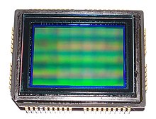
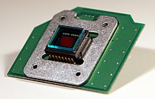
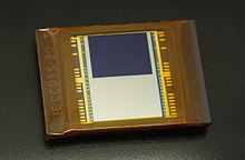
An active-pixel sensor (APS) is an image sensor where each pixel sensor unit cell has a photodetector (typically a pinned photodiode) and one or more active transistors. In a metal–oxide–semiconductor (MOS) active-pixel sensor, MOS field-effect transistors (MOSFETs) are used as amplifiers. There are different types of APS, including the early NMOS APS and the much more common complementary MOS (CMOS) APS, also known as the CMOS sensor, which is widely used in digital camera technologies such as cell phone cameras, web cameras, most modern digital pocket cameras, most digital single-lens reflex cameras (DSLRs), and mirrorless interchangeable-lens cameras (MILCs). CMOS sensors emerged as an alternative to charge-coupled device (CCD) image sensors and eventually outsold them by the mid-2000s.
The term 'active pixel sensor' is also used to refer to the individual pixel sensor itself, as opposed to the image sensor. In this case, the image sensor is sometimes called an active pixel sensor imager, or active-pixel image sensor.
History
Background
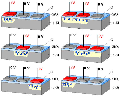
While researching metal–oxide–semiconductor (MOS) technology, Willard Boyle and George E. Smith realized that an electric charge could be stored on a tiny MOS capacitor, which became the basic building block of the charge-couple device (CCD), which they invented in 1969. An issue with CCD technology was that it required the need for nearly perfect charge transfer, which, according to Eric Fossum, "makes their radiation 'soft,' difficult to use under low light conditions, difficult to manufacture in large array sizes, difficult to integrate with on-chip electronics, difficult to use at low temperatures, difficult to use at high frame rates, and difficult to manufacture in non-silicon materials that extend wavelength response."
At RCA Laboratories, a research team including Paul K. Weimer, W.S. Pike and G. Sadasiv in 1969 proposed a solid-state image sensor with scanning circuits using thin-film transistors (TFTs), with photoconductive film used for the photodetector. A low-resolution "mostly digital" N-channel MOSFET (NMOS) imager with intra-pixel amplification, for an optical mouse application, was demonstrated by Richard F. Lyon in 1981. Another type of image sensor technology that is related to the APS is the hybrid infrared focal plane array (IRFPA), designed to operate at cryogenic temperatures in the infrared spectrum. The devices are two chips that are put together like a sandwich: one chip contains detector elements made in InGaAs or HgCdTe, and the other chip is typically made of silicon and is used to read out the photodetectors. The exact date of origin of these devices is classified, but they were in use by the mid-1980s.
A key element of the modern CMOS sensor is the pinned photodiode (PPD). It was invented by Nobukazu Teranishi, Hiromitsu Shiraki and Yasuo Ishihara at NEC in 1980, and then publicly reported by Teranishi and Ishihara with A. Kohono, E. Oda and K. Arai in 1982, with the addition of an anti-blooming structure. The pinned photodiode is a photodetector structure with low lag, low noise, high quantum efficiency and low dark current. The new photodetector structure invented at NEC was given the name "pinned photodiode" (PPD) by B.C. Burkey at Kodak in 1984. In 1987, the PPD began to be incorporated into most CCD sensors, becoming a fixture in consumer electronic video cameras and then digital still cameras. Since then, the PPD has been used in nearly all CCD sensors and then CMOS sensors.
Passive-pixel sensor
The precursor to the APS was the passive-pixel sensor (PPS), a type of photodiode array (PDA). A passive-pixel sensor consists of passive pixels which are read out without amplification, with each pixel consisting of a photodiode and a MOSFET switch. In a photodiode array, pixels contain a p-n junction, integrated capacitor, and MOSFETs as selection transistors. A photodiode array was proposed by G. Weckler in 1968, predating the CCD. This was the basis for the PPS, which had image sensor elements with in-pixel selection transistors, proposed by Peter J.W. Noble in 1968, and by Savvas G. Chamberlain in 1969.
Passive-pixel sensors were being investigated as a solid-state alternative to vacuum-tube imaging devices. The MOS passive-pixel sensor used just a simple switch in the pixel to read out the photodiode integrated charge. Pixels were arrayed in a two-dimensional structure, with an access enable wire shared by pixels in the same row, and output wire shared by column. At the end of each column was a transistor. Passive-pixel sensors suffered from many limitations, such as high noise, slow readout, and lack of scalability. Early photodiode arrays were complex and impractical, requiring selection transistors to be fabricated within each pixel, along with on-chip multiplexer circuits. The noise of photodiode arrays was also a limitation to performance, as the photodiode readout bus capacitance resulted in increased noise level. Correlated double sampling (CDS) could also not be used with a photodiode array without external memory. It was not possible to fabricate active pixel sensors with a practical pixel size in the 1970s, due to limited microlithography technology at the time. Because the MOS process was so variable and MOS transistors had characteristics that changed over time (Vth instability), the CCD's charge-domain operation was more manufacturable than MOS passive pixel sensors.
Active-pixel sensor
The active-pixel sensor consists of active pixels, each containing one or more MOSFET amplifiers which convert the photo-generated charge to a voltage, amplify the signal voltage, and reduce noise. The concept of an active-pixel device was proposed by Peter Noble in 1968. He created sensor arrays with active MOS readout amplifiers per pixel, in essentially the modern three-transistor configuration: the buried photodiode-structure, selection transistor and MOS amplifier.
The MOS active-pixel concept was implemented as the charge modulation device (CMD) by Olympus in Japan during the mid-1980s. This was enabled by advances in MOSFET semiconductor device fabrication, with MOSFET scaling reaching smaller micron and then sub-micron levels during the 1980s to early 1990s. The first MOS APS was fabricated by Tsutomu Nakamura's team at Olympus in 1985. The term active pixel sensor (APS) was coined by Nakamura while working on the CMD active-pixel sensor at Olympus. The CMD imager had a vertical APS structure, which increases fill-factor (or reduces pixel size) by storing the signal charge under an output NMOS transistor. Other Japanese semiconductor companies soon followed with their own active pixel sensors during the late 1980s to early 1990s. Between 1988 and 1991, Toshiba developed the "double-gate floating surface transistor" sensor, which had a lateral APS structure, with each pixel containing a buried-channel MOS photogate and a PMOS output amplifier. Between 1989 and 1992, Canon developed the base-stored image sensor (BASIS), which used a vertical APS structure similar to the Olympus sensor, but with bipolar transistors rather than MOSFETs.
In the early 1990s, American companies began developing practical MOS active pixel sensors. In 1991, Texas Instruments developed the bulk CMD (BCMD) sensor, which was fabricated at the company's Japanese branch and had a vertical APS structure similar to the Olympus CMD sensor, but was more complex and used PMOS rather than NMOS transistors.
CMOS sensor
By the late 1980s to early 1990s, the CMOS process was well-established as a well-controlled stable semiconductor manufacturing process and was the baseline process for almost all logic and microprocessors. There was a resurgence in the use of passive-pixel sensors for low-end imaging applications, while active-pixel sensors began being used for low-resolution high-function applications such as retina simulation and high-energy particle detectors. However, CCDs continued to have much lower temporal noise and fixed-pattern noise and were the dominant technology for consumer applications such as camcorders as well as for broadcast cameras, where they were displacing video camera tubes.
In 1993, the first practical APS to be successfully fabricated outside of Japan was developed at NASA's Jet Propulsion Laboratory (JPL), which fabricated a CMOS compatible APS, with its development led by Eric Fossum. It had a lateral APS structure similar to the Toshiba sensor, but was fabricated with CMOS rather than PMOS transistors. It was the first CMOS sensor with intra-pixel charge transfer.
Fossum, who worked at JPL, led the development of an image sensor that used intra-pixel charge transfer along with an in-pixel amplifier to achieve true correlated double sampling (CDS) and low temporal noise operation, and on-chip circuits for fixed-pattern noise reduction. He also published an extensive 1993 article predicting the emergence of APS imagers as the commercial successor of CCDs. The active pixel sensor (APS) was broadly defined by Fossum in this paper. He classified two types of APS structures, the lateral APS and the vertical APS. He also gave an overview of the history of APS technology, from the first APS sensors in Japan to the development of the CMOS sensor at JPL.
In 1994, Fossum proposed an improvement to the CMOS sensor: the integration of the pinned photodiode (PPD). A CMOS sensor with PPD technology was first fabricated in 1995 by a joint JPL and Kodak team that included Fossum along with P. P. K. Lee, R. C. Gee, R. M. Guidash and T. H. Lee. Between 1993 and 1995, the Jet Propulsion Laboratory developed a number of prototype devices, which validated the key features of the technology. Though primitive, these devices demonstrated good image performance with high readout speed and low power consumption.
In 1995, being frustrated by the slow pace of the technology's adoption, Fossum and his then-wife Dr. Sabrina Kemeny co-founded Photobit Corporation to commercialize the technology. It continued to develop and commercialize APS technology for a number of applications, such as web cams, high speed and motion capture cameras, digital radiography, endoscopy (pill) cameras, digital single-lens reflex cameras (DSLRs) and camera-phones. Many other small image sensor companies also sprang to life shortly thereafter due to the accessibility of the CMOS process and all quickly adopted the active pixel sensor approach.
Photobit's CMOS sensors found their way into webcams manufactured by Logitech and Intel, before Photobit was purchased by Micron Technology in 2001. The early CMOS sensor market was initially led by American manufacturers such as Micron, and Omnivision, allowing the United States to briefly recapture a portion of the overall image sensor market from Japan, before the CMOS sensor market eventually came to be dominated by Japan, South Korea and China. The CMOS sensor with PPD technology was further advanced and refined by R. M. Guidash in 1997, K. Yonemoto and H. Sumi in 2000, and I. Inoue in 2003. This led to CMOS sensors achieve imaging performance on par with CCD sensors, and later exceeding CCD sensors.
By 2000, CMOS sensors were used in a variety of applications, including low-cost cameras, PC cameras, fax, multimedia, security, surveillance, and videophones.
The video industry switched to CMOS cameras with the advent of high-definition video (HD video), as the large number of pixels would require significantly higher power consumption with CCD sensors, which would overheat and drain batteries. Sony in 2007 commercialized CMOS sensors with an original column A/D conversion circuit, for fast, low-noise performance, followed in 2009 by the CMOS back-illuminated sensor (BI sensor), with twice the sensitivity of conventional image sensors and going beyond the human eye.
CMOS sensors went on to have a significant cultural impact, leading to the mass proliferation of digital cameras and camera phones, which bolstered the rise of social media and selfie culture, and impacted social and political movements around the world. By 2007, sales of CMOS active-pixel sensors had surpassed CCD sensors, with CMOS sensors accounting for 54% of the global image sensor market at the time. By 2012, CMOS sensors increased their share to 74% of the market. As of 2017, CMOS sensors account for 89% of global image sensor sales. In recent years, the CMOS sensor technology has spread to medium-format photography with Phase One being the first to launch a medium format digital back with a Sony-built CMOS sensor.
In 2012, Sony introduced the stacked CMOS BI sensor. Fossum now performs research on the Quanta Image Sensor (QIS) technology. The QIS is a revolutionary change in the way we collect images in a camera that is being invented at Dartmouth. In the QIS, the goal is to count every photon that strikes the image sensor, and to provide resolution of 1 billion or more specialized photoelements (called jots) per sensor, and to read out jot bit planes hundreds or thousands of times per second resulting in terabits/sec of data.
Boyd Fowler of OmniVision is known for his work in CMOS image sensor development. His contributions include the first digital-pixel CMOS image sensor in 1994; the first scientific linear CMOS image sensor with single-electron RMS read noise in 2003; the first multi-megapixel scientific area CMOS image sensor with simultaneous high dynamic range (86dB), fast readout (100 frames/second) and ultra-low read noise (1.2e- RMS) (sCMOS) in 2010. He also patented the first CMOS image sensor for inter-oral dental X-rays with clipped corners for better patient comfort.
By the late 2010s CMOS sensors had largely if not completely replaced CCD sensors, as CMOS sensors can not only be made in existing semiconductor production lines, reducing costs, but they also consume less power, just to name a few advantages.
Comparison to CCDs
APS pixels solve the speed and scalability issues of the passive-pixel sensor. They generally consume less power than CCDs, have less image lag, and require less specialized manufacturing facilities. Unlike CCDs, APS sensors can combine the image sensor function and image processing functions within the same integrated circuit. APS sensors have found markets in many consumer applications, especially camera phones. They have also been used in other fields including digital radiography, military ultra high speed image acquisition, security cameras, and optical mice. Manufacturers include Aptina Imaging (independent spinout from Micron Technology, who purchased Photobit in 2001), Canon, Samsung, STMicroelectronics, Toshiba, OmniVision Technologies, Sony, and Foveon, among others. CMOS-type APS sensors are typically suited to applications in which packaging, power management, and on-chip processing are important. CMOS type sensors are widely used, from high-end digital photography down to mobile-phone cameras.
Advantages of CMOS compared with CCD
A primary advantage of a CMOS sensor is that it is typically less expensive to produce than a CCD sensor, as the image capturing and image sensing elements can be combined onto the same IC, with simpler construction required.
A CMOS sensor also typically has better control of blooming (that is, of bleeding of photo-charge from an over-exposed pixel into other nearby pixels).
In three-sensor camera systems that use separate sensors to resolve the red, green, and blue components of the image in conjunction with beam splitter prisms, the three CMOS sensors can be identical, whereas most splitter prisms require that one of the CCD sensors has to be a mirror image of the other two to read out the image in a compatible order. Unlike CCD sensors, CMOS sensors have the ability to reverse the addressing of the sensor elements. CMOS Sensors with a film speed of ISO 4 million exist.
Disadvantages of CMOS compared with CCD
Since a CMOS sensor typically captures a row at a time within approximately 1/60 or 1/50 of a second (depending on refresh rate) it may result in a "rolling shutter" effect, where the image is skewed (tilted to the left or right, depending on the direction of camera or subject movement). For example, when tracking a car moving at high speed, the car will not be distorted but the background will appear to be tilted. A frame-transfer CCD sensor or "global shutter" CMOS sensor does not have this problem; instead it captures the entire image at once into a frame store.
A long-standing advantage of CCD sensors has been their capability for capturing images with lower noise. With improvements in CMOS technology, this advantage has closed as of 2020, with modern CMOS sensors available capable of outperforming CCD sensors.
The active circuitry in CMOS pixels takes some area on the surface which is not light-sensitive, reducing the photon-detection efficiency of the device (back-illuminated sensors can mitigate this problem). But the frame-transfer CCD also has about half non-sensitive area for the frame store nodes, so the relative advantages depend on which types of sensors are being compared.
Architecture
Pixel
The standard CMOS APS pixel consists of a photodetector (pinned photodiode), a floating diffusion, and the so-called 4T cell consisting of four CMOS (complementary metal–oxide–semiconductor) transistors, including a transfer gate, reset gate, selection gate and source-follower readout transistor. The pinned photodiode was originally used in interline transfer CCDs due to its low dark current and good blue response, and when coupled with the transfer gate, allows complete charge transfer from the pinned photodiode to the floating diffusion (which is further connected to the gate of the read-out transistor) eliminating lag. The use of intrapixel charge transfer can offer lower noise by enabling the use of correlated double sampling (CDS). The Noble 3T pixel is still sometimes used since the fabrication requirements are less complex. The 3T pixel comprises the same elements as the 4T pixel except the transfer gate and the photodiode. The reset transistor, Mrst, acts as a switch to reset the floating diffusion to VRST, which in this case is represented as the gate of the Msf transistor. When the reset transistor is turned on, the photodiode is effectively connected to the power supply, VRST, clearing all integrated charge. Since the reset transistor is n-type, the pixel operates in soft reset. The read-out transistor, Msf, acts as a buffer (specifically, a source follower), an amplifier which allows the pixel voltage to be observed without removing the accumulated charge. Its power supply, VDD, is typically tied to the power supply of the reset transistor VRST. The select transistor, Msel, allows a single row of the pixel array to be read by the read-out electronics. Other innovations of the pixels such as 5T and 6T pixels also exist. By adding extra transistors, functions such as global shutter, as opposed to the more common rolling shutter, are possible. In order to increase the pixel densities, shared-row, four-ways and eight-ways shared read out, and other architectures can be employed. A variant of the 3T active pixel is the Foveon X3 sensor invented by Dick Merrill. In this device, three photodiodes are stacked on top of each other using planar fabrication techniques, each photodiode having its own 3T circuit. Each successive layer acts as a filter for the layer below it shifting the spectrum of absorbed light in successive layers. By deconvolving the response of each layered detector, red, green, and blue signals can be reconstructed.
Array
A typical two-dimensional array of pixels is organized into rows and columns. Pixels in a given row share reset lines, so that a whole row is reset at a time. The row select lines of each pixel in a row are tied together as well. The outputs of each pixel in any given column are tied together. Since only one row is selected at a given time, no competition for the output line occurs. Further amplifier circuitry is typically on a column basis.
Size
The size of the pixel sensor is often given in height and width, but also in the optical format.
Lateral and vertical structures
There are two types of active-pixel sensor (APS) structures, the lateral APS and vertical APS. Eric Fossum defines the lateral APS as follows:
A lateral APS structure is defined as one that has part of the pixel area used for photodetection and signal storage, and the other part is used for the active transistor(s). The advantage of this approach, compared to a vertically integrated APS, is that the fabrication process is simpler, and is highly compatible with state-of-the-art CMOS and CCD device processes.
Fossum defines the vertical APS as follows:
A vertical APS structure increases fill-factor (or reduces pixel size) by storing the signal charge under the output transistor.
Thin-film transistors
For applications such as large-area digital X-ray imaging, thin-film transistors (TFTs) can also be used in APS architecture. However, because of the larger size and lower transconductance gain of TFTs compared with CMOS transistors, it is necessary to have fewer on-pixel TFTs to maintain image resolution and quality at an acceptable level. A two-transistor APS/PPS architecture has been shown to be promising for APS using amorphous silicon TFTs. In the two-transistor APS architecture on the right, TAMP is used as a switched-amplifier integrating functions of both Msf and Msel in the three-transistor APS. This results in reduced transistor counts per pixel, as well as increased pixel transconductance gain. Here, Cpix is the pixel storage capacitance, and it is also used to capacitively couple the addressing pulse of the "Read" to the gate of TAMP for ON-OFF switching. Such pixel readout circuits work best with low capacitance photoconductor detectors such as amorphous selenium.
Design variants
Many different pixel designs have been proposed and fabricated. The standard pixel uses the fewest wires and the fewest, most tightly packed transistors possible for an active pixel. It is important that the active circuitry in a pixel take up as little space as possible to allow more room for the photodetector. High transistor count hurts fill factor, that is, the percentage of the pixel area that is sensitive to light. Pixel size can be traded for desirable qualities such as noise reduction or reduced image lag. Noise is a measure of the accuracy with which the incident light can be measured. Lag occurs when traces of a previous frame remain in future frames, i.e. the pixel is not fully reset. The voltage noise variance in a soft-reset (gate-voltage regulated) pixel is , but image lag and fixed pattern noise may be problematic. In rms electrons, the noise is .
Hard reset
Operating the pixel via hard reset results in a Johnson–Nyquist noise on the photodiode of or , but prevents image lag, sometimes a desirable tradeoff. One way to use hard reset is replace Mrst with a p-type transistor and invert the polarity of the RST signal. The presence of the p-type device reduces fill factor, as extra space is required between p- and n-devices; it also removes the possibility of using the reset transistor as an overflow anti-blooming drain, which is a commonly exploited benefit of the n-type reset FET. Another way to achieve hard reset, with the n-type FET, is to lower the voltage of VRST relative to the on-voltage of RST. This reduction may reduce headroom, or full-well charge capacity, but does not affect fill factor, unless VDD is then routed on a separate wire with its original voltage.
Combinations of hard and soft reset
Techniques such as flushed reset, pseudo-flash reset, and hard-to-soft reset combine soft and hard reset. The details of these methods differ, but the basic idea is the same. First, a hard reset is done, eliminating image lag. Next, a soft reset is done, causing a low noise reset without adding any lag. Pseudo-flash reset requires separating VRST from VDD, while the other two techniques add more complicated column circuitry. Specifically, pseudo-flash reset and hard-to-soft reset both add transistors between the pixel power supplies and the actual VDD. The result is lower headroom, without affecting fill factor.


