The silicon atoms on the surface of a crystal of silicon carbide (SiC). Image obtained using an STM.
An STM image of a single-walled carbon nanotube
STM is based on the concept of quantum tunneling. When a conducting tip is brought very near to the surface to be examined, a bias (voltage difference) applied between the two can allow electrons to tunnel through the vacuum between them. The resulting tunneling current is a function of tip position, applied voltage, and the local density of states (LDOS) of the sample.[4] Information is acquired by monitoring the current as the tip's position scans across the surface, and is usually displayed in image form. STM can be a challenging technique, as it requires extremely clean and stable surfaces, sharp tips, excellent vibration control, and sophisticated electronics, but nonetheless many hobbyists have built their own.[6]
Scanning tunneling microscope operating principle
Procedure
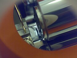
A close-up of a simple scanning tunneling microscope head using a platinum–iridium tip.
First, a voltage bias is applied and the tip is brought close to the sample by coarse sample-to-tip control, which is turned off when the tip and sample are sufficiently close. At close range, fine control of the tip in all three dimensions when near the sample is typically piezoelectric, maintaining tip-sample separation W typically in the 4-7 Å (0.4-0.7 nm) range, which is the equilibrium position between attractive (3
In this situation, the voltage bias will cause electrons to tunnel between the tip and sample, creating a current that can be measured. Once tunneling is established, the tip's bias and position with respect to the sample can be varied (with the details of this variation depending on the experiment) and data are obtained from the resulting changes in current.
If the tip is moved across the sample in the x-y plane, the changes in surface height and density of states causes changes in current. These changes are mapped in images. This change in current with respect to position can be measured itself, or the height, z, of the tip corresponding to a constant current can be measured.[4] These two modes are called constant height mode and constant current mode, respectively. In constant current mode, feedback electronics adjust the height by a voltage to the piezoelectric height control mechanism.[7] This leads to a height variation and thus the image comes from the tip topography across the sample and gives a constant charge density surface; this means contrast on the image is due to variations in charge density.[8] In constant height mode, the voltage and height are both held constant while the current changes to keep the voltage from changing; this leads to an image made of current changes over the surface, which can be related to charge density.[8] The benefit to using a constant height mode is that it is faster, as the piezoelectric movements require more time to register the height change in constant current mode than the current change in constant height mode.[8] All images produced by STM are grayscale, with color optionally added in post-processing in order to visually emphasize important features.
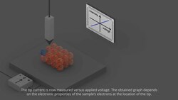
In addition to scanning across the sample, information on the electronic structure at a given location in the sample can be obtained by sweeping voltage and measuring current at a specific location.[3] This type of measurement is called scanning tunneling spectroscopy (STS) and typically results in a plot of the local density of states as a function of energy within the sample. The advantage of STM over other measurements of the density of states lies in its ability to make extremely local measurements: for example, the density of states at an impurity site can be compared to the density of states far from impurities.[9]
Frame rates of at least 25 Hz enable so called video-rate STM.[10][11] Framerates up to 80 Hz are possible with fully working feedback that adjusts the height of the tip.[12] Due to the line-by-line scanning motion, a proper comparison on the speed requires not only the framerate, but also the number of pixels in an image: with a framerate of 10 Hz and 100x100 pixels the tip moves with a line frequency of 1 kHz, whereas it moves with only with 500 Hz, when measuring with a faster framerate of 50 Hz but only 10x10 pixels. Video-rate STM can be used to scan surface diffusion.[13]
Instrumentation
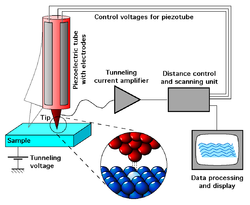
Schematic view of an STM
The components of an STM include scanning tip, piezoelectric controlled height and x,y scanner, coarse sample-to-tip control, vibration isolation system, and computer.[7]
The resolution of an image is limited by the radius of curvature of the scanning tip of the STM. Additionally, image artifacts can occur if the tip has two tips at the end rather than a single atom; this leads to “double-tip imaging,” a situation in which both tips contribute to the tunneling.[3] Therefore, it has been essential to develop processes for consistently obtaining sharp, usable tips. Recently, carbon nanotubes have been used in this instance.[14]
The tip is often made of tungsten or platinum-iridium, though gold is also used.[3] Tungsten tips are usually made by electrochemical etching, and platinum-iridium tips by mechanical shearing.[3]
Due to the extreme sensitivity of tunnel current to height, proper vibration insulation or an extremely rigid STM body is imperative for obtaining usable results. In the first STM by Binnig and Rohrer, magnetic levitation was used to keep the STM free from vibrations; now mechanical spring or gas spring systems are often used.[4] Additionally, mechanisms for reducing eddy currents are sometimes implemented.
Maintaining the tip position with respect to the sample, scanning the sample and acquiring the data is computer controlled.[7] The computer may also be used for enhancing the image with the help of image processing[15][16] as well as performing quantitative measurements.[17][18]
Nanomanipulation via STM of a self-assembled organic semiconductor monolayer (here: PTCDA molecules) on graphite, in which the logo of the Center for NanoScience (CeNS), LMU has been written.
Image of a graphite surface at an atomic level obtained by an STM.
Many other microscopy techniques have been developed based upon STM. These include photon scanning microscopy (PSTM), which uses an optical tip to tunnel photons;[3] scanning tunneling potentiometry (STP), which measures electric potential across a surface;[3] spin polarized scanning tunneling microscopy (SPSTM), which uses a ferromagnetic tip to tunnel spin-polarized electrons into a magnetic sample,[19] and atomic force microscopy (AFM), in which the force caused by interaction between the tip and sample is measured.
Other STM methods involve manipulating the tip in order to change the topography of the sample. This is attractive for several reasons. Firstly the STM has an atomically precise positioning system which allows very accurate atomic scale manipulation. Furthermore, after the surface is modified by the tip, it is a simple matter to then image with the same tip, without changing the instrument. IBM researchers developed a way to manipulate xenon atoms adsorbed on a nickel surface.[3] This technique has been used to create electron "corrals" with a small number of adsorbed atoms, which allows the STM to be used to observe electron Friedel oscillations on the surface of the material. Aside from modifying the actual sample surface, one can also use the STM to tunnel electrons into a layer of electron beam photoresist on a sample, in order to do lithography. This has the advantage of offering more control of the exposure than traditional electron beam lithography. Another practical application of STM is atomic deposition of metals (gold, silver, tungsten, etc.) with any desired (pre-programmed) pattern, which can be used as contacts to nanodevices or as nanodevices themselves.
Variable temperature STM was used to investigate temperature dependency of molecular rotations on single crystalline surfaces.[20] Rotating molecules appear blurred compared to non-rotating ones.
Recently groups have found they can use the STM tip to rotate individual bonds within single molecules.[citation needed] The electrical resistance of the molecule depends on the orientation of the bond, so the molecule effectively becomes a molecular switch.
Principle of operation
The first STM produced commercially, 1986.
Tunneling is a functioning concept that arises from quantum mechanics. Classically, an object hitting an impenetrable barrier will not pass through. In contrast, objects with a very small mass, such as the electron, have wavelike characteristics which permit such an event, referred to as tunneling.
Electrons behave as beams of energy, and in the presence of a potential U(z), assuming 1-dimensional case, the energy levels ψn(z) of the electrons are given by solutions to Schrödinger’s equation,
 .[4]
.[4]Knowing the wave function allows one to calculate the probability density for that electron to be found at some location. In the case of tunneling, the tip and sample wave functions overlap such that when under a bias, there is some finite probability to find the electron in the barrier region and even on the other side of the barrier.[4] Let us assume the bias is V and the barrier width is W. This probability, P, that an electron at z=0 (left edge of barrier) can be found at z=W (right edge of barrier) is proportional to the wave function squared,
-
.[4]
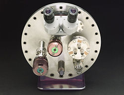
A large scanning tunneling microscope, in the labs of the London Centre for Nanotechnology
However, tunneling does require that there be an empty level of the same energy as the electron for the electron to tunnel into on the other side of the barrier. It is because of this restriction that the tunneling current can be related to the density of available or filled states in the sample. The current due to an applied voltage V (assume tunneling occurs sample to tip) depends on two factors: 1) the number of electrons between Ef and eV in the sample, and 2) the number among them which have corresponding free states to tunnel into on the other side of the barrier at the tip.[4] The higher the density of available states the greater the tunneling current. When V is positive, electrons in the tip tunnel into empty states in the sample; for a negative bias, electrons tunnel out of occupied states in the sample into the tip.[4]
Mathematically, this tunneling current is given by
-
.
-
,
This approach fails to account for the rate at which electrons can pass the barrier. This rate should affect the tunnel current, so it can be treated using the Fermi's golden rule with the appropriate tunneling matrix element. John Bardeen solved this problem in his study of the metal-insulator-metal junction.[21] He found that if he solved Schrödinger’s equation for each side of the junction separately to obtain the wave functions ψ and χ for each electrode, he could obtain the tunnel matrix, M, from the overlap of these two wave functions.[4] This can be applied to STM by making the electrodes the tip and sample, assigning ψ and χ as sample and tip wave functions, respectively, and evaluating M at some surface S between the metal electrodes, where z=0 at the sample surface and z=W at the tip surface.[4]
Now, Fermi’s Golden Rule gives the rate for electron transfer across the barrier, and is written
-
,
-
,
Summing over all the states gives the tunneling current as
-
,


