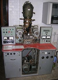
An electron microprobe (EMP), also known as an electron probe microanalyzer (EPMA) or electron micro probe analyzer (EMPA), is an analytical tool used to non-destructively determine the chemical composition of small volumes of solid materials. It works similarly to a scanning electron microscope: the sample is bombarded with an electron beam, emitting x-rays at wavelengths characteristic to the elements being analyzed. This enables the abundances of elements present within small sample volumes (typically 10-30 cubic micrometers or less) to be determined, when a conventional accelerating voltage of 15-20 kV is used. The concentrations of elements from lithium to plutonium may be measured at levels as low as 100 parts per million (ppm), material dependent, although with care, levels below 10 ppm are possible. The ability to quantify lithium by EPMA became a reality in 2008.
History
The electron microprobe (electron probe microanalyzer) developed from two technologies: electron microscopy — using a focused high energy electron beam to impact a target material, and X-ray spectroscopy — identification of the photons scattered from the electron beam impact, with the energy/wavelength of the photons characteristic of the atoms excited by the incident electrons. Ernst Ruska and Max Knoll are associated with the prototype electron microscope in 1931. Henry Moseley was involved in the discovery of the direct relationship between the wavelength of X-rays and the identity of the atom from which it originated.
There have been at several historical threads to electron beam microanalysis. One was developed by James Hillier and Richard Baker at RCA. In the early 1940s, they built an electron microprobe, combining an electron microscope and an energy loss spectrometer. A patent application was filed in 1944. Electron energy loss spectroscopy is very good for light element analysis and they obtained spectra of C-Kα, N-Kα and O-Kα radiation. In 1947, Hiller patented the concept of using an electron beam to produce analytical X-rays, but never constructed a working model. His design proposed using Bragg diffraction from a flat crystal to select specific X-ray wavelengths and a photographic plate as a detector. However, RCA had no interest in commercializing this invention.
A second thread developed in France in the late 1940s. In 1948–1950, Raimond Castaing, supervised by André Guinier, built the first electron “microsonde électronique” (electron microprobe) at ONERA. This microprobe produced an electron beam diameter of 1-3 μm with a beam current of ~10 nanoamperes (nA) and used a Geiger counter to detect the X-rays produced from the sample. However, the Geiger counter could not distinguish X-rays produced from specific elements and in 1950, Castaing added a quartz crystal between the sample and the detector to permit wavelength discrimination. He also added an optical microscope to view the point of beam impact. The resulting microprobe was described in Castaing's 1951 PhD Thesis, translated into English by Pol Duwez and David Wittry, in which he laid the foundations of the theory and application of quantitative analysis by electron microprobe, establishing the theoretical framework for the matrix corrections of absorption and fluorescence effects. Castaing (1921-1999) is considered the father of electron microprobe analysis.
The 1950s was a decade of great interest in electron beam X-ray microanalysis, following Castaing's presentations at the First European Microscopy Conference in Delft in 1949 and then at the National Bureau of Standards conference on Electron Physics in Washington, DC, in 1951, as well as at other conferences in the early to mid-1950s. Many researchers, mainly material scientists, developed their own experimental electron microprobes, sometimes starting from scratch, but many times using surplus electron microscopes.
One of the organizers of the Delft 1949 Electron Microscopy conference was Vernon Ellis Cosslett at the Cavendish Laboratory at Cambridge University, a center of research on electron microscopy, as well as scanning electron microscopy with Charles Oatley as well as X-ray microscopy with Bill Nixon. Peter Duncumb combined all three technologies and developed a scanning electron X-ray microanalyzer for his PhD thesis (1957), which was commercialized as the Cambridge MicroScan.
Pol Duwez, a Belgian material scientist who fled the Nazis and settled at the California Institute of Technology and collaborated with Jesse DuMond, encountered André Guinier on a train in Europe in 1952, where he learned of Castaing's new instrument and the suggestion that Caltech build a similar instrument. David Wittry was hired to build such an instrument as his PhD thesis, which he completed in 1957. It became the prototype for the ARL EMX electron microprobe.
During the late 1950s and early 1960s there were over a dozen other laboratories in North America, the United Kingdom, Europe, Japan and the USSR developing electron beam X-ray microanalyzers.
The first commercial electron microprobe, the "MS85" was produced by CAMECA (France) in 1956. It was soon followed in the early-mid 1960s by microprobes from other companies; however, all companies except CAMECA, JEOL and Shimadzu Corporation went out of business. In addition, many researchers build electron microprobes in their labs. Significant subsequent improvements and modifications to microprobes included scanning the electron beam to make X-ray maps (1960), the addition of solid state EDS detectors (1968) and the development of synthetic multilayer diffracting crystals for analysis of light elements (1984). Later, CAMECA pioneered manufacturing a shielded electron microprobe for nuclear applications. Several advances in CAMECA instruments in recent decades expanded the range of applications on metallurgy, electronics, geology, mineralogy, nuclear plants, trace elements, and dentistry.
Operation
A beam of electrons is fired at a sample. The beam causes each element in the sample to emit X-rays at a characteristic frequency; the X-rays can then be detected by the electron microprobe. The size and current density of the electron beam determines the trade-off between resolution and scan time and/or analysis time.
Detailed description
Low-energy electrons are produced from a tungsten filament, a lanthanum hexaboride crystal cathode or a field emission electron source and accelerated by a positively biased anode plate to 3 to 30 thousand electron volts (keV). The anode plate has central aperture and electrons that pass through it are collimated and focused by a series of magnetic lenses and apertures. The resulting electron beam (approximately 5 nm to 10 μm diameter) may be rastered across the sample or used in spot mode to produce excitation of various effects in the sample. Among these effects are: phonon excitation (heat), cathodoluminescence (visible light fluorescence), continuum X-ray radiation (bremsstrahlung), characteristic X-ray radiation, secondary electrons (plasmon production), backscattered electron production, and Auger electron production.
When the beam electrons (and scattered electrons from the sample) interact with bound electrons in the innermost electron shells of the atoms of the various elements in the sample, they can scatter the bound electrons from the electron shell producing a vacancy in that shell (ionization of the atom). This vacancy is unstable and must be filled by an electron from either a higher energy bound shell in the atom (producing another vacancy which is in turn filled by electrons from yet higher energy bound shells) or by unbound electrons of low energy. The difference in binding energy between the electron shell in which the vacancy was produced and the shell from which the electron comes to fill the vacancy is emitted as a photon. The energy of the photon is in the X-ray region of the electromagnetic spectrum. As the electron structure of each element is unique, the series X-ray line energies produced by vacancies in the innermost shells is characteristic of that element, although lines from different elements may overlap. As the innermost shells are involved, the X-ray line energies are generally not affected by chemical effects produced by bonding between elements in compounds except in low atomic number (Z) elements ( B, C, N, O and F for Kalpha and Al to Cl for Kbeta) where line energies may be shifted as a result of the involvement of the electron shell from which vacancies are filled in chemical bonding.
The characteristic X-rays are used for chemical analysis. Specific X-ray wavelengths or energies are selected and counted, either by wavelength dispersive X-ray spectroscopy (WDS) or energy dispersive X-ray spectroscopy (EDS). WDS utilizes Bragg diffraction from crystals to select X-ray wavelengths of interest and direct them to gas-flow or sealed proportional detectors. In contrast, EDS uses a solid state semiconductor detector to accumulate X-rays of all wavelengths produced from the sample. While EDS yields more information and typically requires a much shorter counting time, WDS is generally more precise with lower limits of detection due to its superior X-ray peak resolution and greater peak to background ratio.
Chemical composition is determined by comparing the intensities of characteristic X-rays from the sample with intensities from standards of known composition. Counts from the sample must be corrected for matrix effects (depth of production of the X-rays, absorption and secondary fluorescence) to yield quantitative chemical compositions. The resulting chemical data is gathered in textural context. Variations in chemical composition within a material (zoning), such as a mineral grain or metal, can be readily determined.
Volume from which chemical information is gathered (volume of X-rays generated) is 0.3 – 3 cubic micrometers.
Limitations
- WDS cannot determine elements below number 3 (lithium). This restricts WDS when analyzing geologically important elements such as H, Li, and Be.
- Despite the improved spectral resolution of elemental peaks, some peaks exhibit significant overlap that causes analytical challenges (e.g., VKα and TiKβ). WDS analyses are unable to distinguish the valence states of elements (e.g. Fe2+ vs. Fe3+) which must be obtained by other techniques such as Mössbauer spectroscopy or electron energy loss spectroscopy.
- Element isotopes cannot be determined by WDS, but are most commonly obtained with a mass spectrometer.
Applications
Materials science and engineering


The technique is commonly used for analyzing the chemical composition of metals, alloys, ceramics, and glasses. It is particularly useful for assessing the composition of individual particles or grains and chemical changes on the scale of a few micrometres to millimeters. The electron microprobe is widely used for research, quality control, and failure analysis.
Mineralogy and petrology
This technique is most commonly used by mineralogists and petrologists. Most rocks are aggregates of small mineral grains. These grains may preserve chemical information acquired during their formation and subsequent alteration. This information may illuminate geologic processes such as crystallization, lithification, volcanism, metamorphism, orogenic events (mountain building), and plate tectonics. This technique is also used for the study of extraterrestrial rocks (meteorites), and provides chemical data which is vital to understanding the evolution of the planets, asteroids, and comets.
The change in elemental composition from the center (also known as core) to the edge (or rim) of a mineral can yield information about the history of the crystal's formation, including the temperature, pressure, and chemistry of the surrounding medium. Quartz crystals, for example, incorporate a small, but measurable amount of titanium into their structure as a function of temperature, pressure, and the amount of titanium available in their environment. Changes in these parameters are recorded by titanium as the crystal grows.
Paleontology
In exceptionally preserved fossils, such as those of the Burgess shale, soft parts of organisms may be preserved. Since these fossils are often compressed into a planar film, it can be difficult to distinguish the features: a famous example is the triangular extensions in Opabinia, which were interpreted as either legs or extensions of the gut. Elemental mapping showed that their composition was similar to the gut, favoring that interpretation. Because of the thinness of carbon films, only low voltages (5-15 kV) can be used on them.
Meteorite analysis
The chemical composition of meteorites can be analyzed quite accurately using EPMA. This can reveal much about the conditions that existed in the early Solar System.