The problem of mental causation is a conceptual issue in the philosophy of mind. That problem, in short, is how to account for the common sense idea that intentional thoughts or intentional mental states
are causes of intentional actions. The problem divides into several
distinct sub-problems, including the problem of causal exclusion, the
problem of anomalism, and the problem of externalism. However, the
sub-problem which has attracted most attention in the philosophical
literature is arguably the exclusion problem.
Description
The basic problem of mental causation is an intuitive one: on the face of it, it seems that mental events
cause physical events (and vice versa), but how can mental events have
any causal effect on physical events? Suppose that a person, John,
orders dessert after dinner. It seems that at least one cause for such a
physical, behavioral event is that John desired to have dessert and
believed that by ordering dessert he would be able to soon have dessert.
But, how can such mental events as beliefs and desires cause John's
mouth to move in such a way that he orders dessert?
Sub-problems of mental causation
Exclusion problem
What follows is a summary of the causal exclusion problem
in its simplest form, and it is merely one of several possible
formulations.
To the extent that we do not have to go
outside human physiology in order to trace the causal antecedents of any
bodily movement, intentional action can be fully causally explained by
the existence of these physiological antecedents alone.
No mention of mental states need enter into the explanation. This
troubles philosophers because intuitively it seems that mental states
are crucial in causing a person to act (for example, their beliefs and
desires). But, given that physiological facts are sufficient to account
for action, mental states appear to be superfluous; they are at risk of
being causally and explanatorily irrelevant with respect to human action
(Yoo 2006, p.§3b.iii).
Many philosophers consider this apparent irrelevance to be a
highly counter-intuitive and undesirable position to take. It
ultimately leads to epiphenomenalism—the
view that mental events or states are causally irrelevant, they are
merely after effects that play no role in any causal chains whatsoever. Thomas Huxley
famously noted that epiphenomenalism treats mental states like the
steam coming off a train: it plays no causal role in the train's moving
forward, it is merely an "emergent property" of the actual causation
occurring in the engine (Walter 2003, p.§2).
Problem of anomalism
Another problem with mental causation is that mental events
seem anomalous in the sense that there are no scientific laws that
mental states can figure into without having exceptions. There are no
"strict" laws, and mental events must factor into strict laws in order
to fit respectably into the causal order described by current science
[see (Davidson 1970)].
In short, one response has been to deny that psychological laws involving mental states require strict, exceptionless laws. Jerry Fodor argues that non-basic (or "special") sciences do not in fact require strict laws (Fodor 1980). In current practice, special sciences (for example, biology and chemistry) have ceteris paribus
laws (or laws with "all else being equal" clauses), according to which
there are exceptions. However, only in the basic sciences (physics) are
there strict, exceptionless laws. Thus, although mental states are
anomalous, they can still figure into scientifically respectable laws of
psychology.
Problem of externalism
In the latter half of the twentieth century externalism about meanings
became espoused by many philosophers. Externalism is roughly the view
that certain parts of an individual's environment play a crucial role in
the meaning of at least some of an individual's words [see (Putnam 1975) and (Burge 1979)]. A thesis about meaning affects the mind insofar as our thoughts are about
things in the world. A common view in the philosophy of mind is that at
least certain mental states have intentional content in this sense. For
example, one's belief that water is wet has the semantic content of water is wet.
The thought is about water and the fact that it is wet. But, if
externalism is true—if some of the contents of one's thoughts are
constituted at least in part by factors external to one's mind—then
there is yet another difficulty in explaining how mental states can
cause physical states (Yoo 2006, p.§3b.ii)].
Some have claimed that while the mental and the physical
are quite different things, they can nonetheless causally interact with
one another, a view going back to Descartes [(Descartes & 1642/1986), especially meditations II & VI]. This view is known as interactionist dualism.
The major problem that interactionist dualism faces is that of
explicating a satisfactory notion of causation according to which
non-spatial events, such as mental events, can causally interact with
physical events. According to the current mainstream scientific
world-view, the physical realm is causally closed,
in that causal relationships only hold among physical events in the
physical realm. Given these types of considerations, some argue that it
is appropriate to say that the main assumptions in interactionist
dualism generate the problem of mental causation rather than solve it
(see (Yoo 2006, p.§1a).
The other major option is to assert that mental events are either (at least contingently) identical to physical events, or supervene on physical events. Views that fall under this general heading are called physicalism or materialism. But, such views require a particular theory to explain how mental events are physical in nature. One such theory is behaviorism. Behaviorists, in general, argue that mental events are merely dispositions to behave in certain ways. Another theory is the identity theory, according to which mental events are (either type- or token-) identical to physical events. A more recent view, known as functionalism,
claims that mental events are individuated (or constituted by) the
causal role they play. As such, mental events would fit directly into
the causal realm, as they are simply certain causal (or functional)
roles.
Idealist solutions
Popper's three-world formulation
Related to dualism above, a more general and somewhat differently posed approach to mental causation is provided by Karl Popper's three worlds. Popper split the world into three categories:
The mental or psychological world, the world of our
feelings of pain and of pleasure, of our thoughts, of our decisions, of
our perceptions and our observations; in other words, the world of
mental or psychological states or processes, or of subjective
experiences.
The world of products of the human mind, including art, science, and religion.
World 3 includes physical theory as a particular case. But
World 3 is a creation of the human imagination, and such acts of
imagination are a part of World 2. Accordingly, one could argue that the
physical notion of causality is a child of the imagination, and
although causation has its successes in describing World 1, it may not
apply to World 2 or World 3. The subjective aspects of theories
contained in World 3 are not readily framed within the third-person
perspective of science used to explain World 1.
From this perspective, it is hubris to suppose that the
methods successful in describing World 1, in particular to suppose the
notions of cause and effect, invented
by World 2 in its creation of the theory of World 3 used to explain
World 1, have direct application to Worlds 2 and 3 themselves, and
control mental agency.
Psychological nativism
A still different approach to mental causation is based
upon the philosophies of Kant, Chomsky and Pinker. These philosophers
stress the impact of built-in aspects of mind, studied in the field of psychological nativism.
Immanuel Kant (1724–1804) pointed out that we all shape our experience of things through the filter of our mind, a view sometimes called epistemological solipsism. The mind shapes that experience, and among other things, Kant believed the concepts of space and time were programmed into the human brain, as was the notion of cause and effect. We never have direct experience of things, the noumenal world, and what we do experience is the phenomenal
world as conveyed by our senses, this conveyance processed by the
machinery of the mind and nervous system. Kant focused upon this
processing. Kant believed in a priori knowledge arrived at independent of experience, so-called synthetica priori
knowledge. In particular, he thought that by introspection some aspects
of the filtering mechanisms of the mind/brain/nervous system could be
discovered. The following observations summarize Kant's views upon the subject-object problem, called Kant's Copernican revolution:
"It has hitherto
been assumed that our cognition must conform to the objects; but all
attempts to ascertain anything about these objects a priori, by
means of conceptions, and thus to extend the range of our knowledge,
have been rendered abortive by this assumption. Let us then make the
experiment whether we may not be more successful in metaphysics, if we
assume that the objects must conform to our cognition. This appears, at
all events, to accord better with the possibility of our gaining the end
we have in view, that is to say, of arriving at the cognition of
objects a priori, of determining something with respect to these
objects, before they are given to us. We here propose to do just what
Copernicus did in attempting to explain the celestial movements. When he
found that he could make no progress by assuming that all the heavenly
bodies revolved round the spectator, he reversed the process, and tried
the experiment of assuming that the spectator revolved, while the stars
remained at rest. We may make the same experiment with regard to the
intuition of objects."
—Immanuel Kant, English translation by John Meiklejohn of The Critique of Pure Reason (1. edition 1781, April 23, 1787 Immanuel Kant, Preface to the 2. edition)
Although Kant has posed the issue of built-in aspects of
mind, the particulars that depend upon the science of his day have
become outmoded. A more recent approach to these limitations is proposed
by Noam Chomsky and Steven Pinker. Like Kant, Noam Chomsky
raised the issue of the mind's inherent programming. Chomsky selected
as a particular example the acquiring of language by children. Of course, language is indispensable in the formulation and communication of our perceptions of the objective world:
"People do not
think in English or Chinese or Apache; they think in a language of
thought. This language of thought probably looks a bit like all these
languages;...But compared with any given language, mentalese must be
richer in some ways and simpler in others."
—Steven Pinker, The Language Instinct, p. 72
Chomsky marshaled evidence that a child's rapid mastery of
the complexity of language indicated an innate ability programmed into
the development of the human mind from birth that could not be explained
by the "blank slate"
view of the infant mind. Rather, the mind has a built-in propensity to
process symbolic representations. The origins of this ability were
sought by Steven Pinker in a Darwinian struggle that established the survival value of the ability to communicate. According to Pinker, Charles Darwin
himself "concluded that language ability is 'an instinctive tendency to
acquire an art', a design that is not peculiar to humans but seen in
other species such as song-learning birds." This observation is strongly
supported by research on crows.
This work can be taken to suggest that although a physical
theory is an intermediary between our observations and our notions of
connections between them, it is an elaborate mental construction that is
a meld of the way the mind works and objective observations. Although a
physical theory is used to determine connections about objective
events, the specific form of the theoretical construct is a product of
subjective activities, and this particular form may well involve the
workings of the brain. Perhaps some aspects of the universe's operation
can be expressed in terms of mental constructs, but this process is
analogous with the expression of a computer algorithm in terms of assembly language instructions peculiar to a particular computer, a translation by a compiler of the general statement of an algorithm into specific tiny steps that particular computer can handle.
From this standpoint, as with the philosophy of Kant, the
first-person active actions of mental causation may involve innate
workings of the brain itself.
Solar cells are often classified into generations based on
the kinds of light-absorbing layers used to make them. The most
well-established or first-generation solar cells are made of single- or multi-crystalline silicon. This is the dominant technology currently used in most solar PV systems. Most types of thin-film solar cells are classified as second generation, made using thin layers of materials like amorphous silicon (a-Si), cadmium telluride (CdTe), copper indium gallium selenide (CIGS), or gallium arsenide (GaAs). Solar cells made with newer, less established materials are classified as third-generation or emerging solar cells. This includes some innovative thin-film technologies, such as perovskite, dye-sensitized, quantum dot, organic, and CZTS thin-film solar cells.
Thin-film cells have several advantages over
first-generation silicon solar cells, including being lighter and more
flexible due to their thin construction. This makes them suitable for
use in building-integrated photovoltaics
and as semi-transparent photovoltaic glazing material that can be
laminated onto windows. Other commercial applications use rigid thin
film solar panels (interleaved between two panes of glass) in some of the world's largestphotovoltaic power stations.
Additionally, the materials used in thin-film solar cells are typically
produced using simple and scalable methods more cost-effective than
first-generation cells, leading to lower environmental impacts like greenhouse gas (GHG) emissions in many cases. Thin-film cells also typically outperform renewable and non-renewable sources for electricity generation in terms of human toxicity and heavy-metal emissions.
Despite initial challenges with efficient light conversion,
especially among third-generation PV materials, as of 2023 some
thin-film solar cells have reached efficiencies of up to 29.1% for
single-junction thin-film GaAs cells, exceeding the maximum of 26.1%
efficiency for standard single-junction first-generation solar cells. Multi-junctionconcentrator cells incorporating thin-film technologies have reached efficiencies of up to 47.6% as of 2023.
Many thin-film technologies have been found to have shorter operational
lifetimes and larger degradation rates than first-generation cells in accelerated life testing, which has contributed to their somewhat limited deployment. Globally, the PV market share of thin-film technologies remains around 5% as of 2023. However, thin-film technology has become considerably more popular in
the United States, where CdTe cells alone accounted for 29% of new utility-scale deployment in 2021.
History
Market-share of thin-film technologies in terms of annual production since 1980
Early research into thin-film solar cells began in the 1970s. In 1970, Zhores Alferov's team at Ioffe Institute created the first gallium arsenide (GaAs) solar cells, later winning the 2000 Nobel prize in Physics for this and other work. Two years later in 1972, Prof. Karl Böer founded the Institute of Energy Conversion
(IEC) at the University of Delaware to further thin-film solar
research. The institute first focused on copper sulfide/cadmium sulfide
(Cu2S/CdS) cells and later expanded to zinc phosphide (Zn3P2) and amorphous silicon (a-Si) thin-films as well in 1975. In 1973, the IEC debuted a solar-powered house, Solar One, in the first
example of residential building-integrated photovoltaics. In the next decade, interest in thin-film technology for commercial use and aerospace applications increased significantly, with several companies beginning
development of amorphous silicon thin-film solar devices. Thin-film solar efficiencies rose to 10% for Cu2S/CdS in 1980, and in 1986 ARCO Solar launched the first commercially available thin-film solar cell, the G-4000, made from amorphous silicon.
In the 1990s and 2000s, thin-film solar cells saw
significant increases in maximum efficiencies and expansion of existing
thin-film technologies into new sectors. In 1992, a thin-film solar cell
with greater than 15% efficiency was developed at University of South Florida. Only seven years later in 1999, the U.S. National Renewable Energy Laboratory and Spectrolab collaborated on a three-junction gallium arsenide solar cell that reached 32% efficiency. That same year, Kiss + Cathcart designed transparent thin-film solar cells for some of the windows in 4 Times Square, generating enough electricity to power 5-7 houses. In 2000, BP Solar introduced two new commercial solar cells based on thin-film technology. In 2001, the first organic thin-film solar cells were developed at the Johannes Kepler University of Linz. In 2005, GaAs solar cells got even thinner with the first free-standing (no substrate) cells introduced by researchers at Radboud University.
This was also a time of significant advances in the
exploration of new third-generation solar materials–materials with the
potential to overcome theoretical efficiency limits for traditional
solid-state materials. In 1991, the first high-efficiency dye-sensitized solar cell
was developed, replacing the ordinary solid semiconducting (active)
layer of the cell with a liquid electrolyte mixture containing
light-absorbing dye. In the early 2000s, development of quantum dot solar cells began, technology later certified by the National Renewable Energy Laboratory in 2011. In 2009, researchers at the University of Tokyo reported a new type solar cell using perovskites as the active layer and achieving over 3% efficiency, building on Murase Chikao's 1999 work which created a perovskite layer capable of absorbing light.
In the 2010s and early 2020s, innovation in thin-film solar
technology has included efforts to expand third-generation solar
technology to new applications and to decrease production costs, as well
as significant efficiency improvements for both second and third
generation materials. In 2015, Kyung-In Synthetic released the first inkjet solar cells, flexible solar cells made with industrial printers. In 2016, Vladimir Bulović's Organic and Nanostructured Electronics (ONE) Lab at the Massachusetts Institute of Technology (MIT) created thin-film cells light enough to sit on top of soap bubbles. In 2022, the same group introduced flexible organic thin-film solar cells integrated into fabric.
Thin-film solar technology captured a peak global market
share of 32% of the new photovoltaic deployment in 1988 before declining
for several decades and reaching another, smaller peak of 17% again in
2009. Market share then steadily declined to 5% in 2021 globally, however thin-film technology captured approximately 19% of the total
U.S. market share in the same year, including 30% of utility-scale
production.
In a typical solar cell, the photovoltaic effect is used to generate electricity from sunlight. The light-absorbing or "active layer" of the solar cell is typically a semiconducting material, meaning that there is a gap in its energy spectrum between the valence band of localized electrons around host ions
and the conduction band of higher-energy electrons which are free to
move throughout the material. For most semiconducting materials at room temperature,
electrons which have not gained extra energy from another source will
exist largely in the valence band, with few or no electrons in the
conduction band. When a solar photon reaches the semiconducting active
layer in a solar cell, electrons in the valence band can absorb the
energy of the photon and be excited into the conduction band, allowing them to move freely throughout the material. When this happens, an empty electron state (or hole) is left behind in the valence band. Together, the conduction band electron and the valence band hole are called an electron-hole pair. Both the electron and the hole in the electron-hole pair can move freely throughout the material as electricity. However, if the electron-hole pair is not separated, the electron and hole can recombine into the lower-energy original state, releasing a photon of the corresponding energy. In thermodynamic equilibrium,
the forward process (absorbing a photon to excite an electron-hole
pair) and reverse process (emitting a photon to destroy an electron-hole
pair) must occur at the same rate by the principle of detailed balance.
Therefore, to construct a solar cell from a semiconducting material and
extract current during the excitation process, the electron and hole of
the electron-hole pair must be separated. This can be achieved in a
variety of different ways, but the most common is with a p-n junction, where a positively doped (p-type) semiconducting layer and a negatively doped (n-type) semiconducting layer meet, creating a chemical potential difference which draws electrons one direction and holes the other, separating the electron-hole pair. This may instead be achieved using metal contacts with different work functions, as in a Schottky-junction cell.
In a thin-film solar cell, the process is largely the same
but the active semiconducting layer is made much thinner. This may be
made possible by some intrinsic property of the semiconducting material
used that allows it to convert a particularly large number of photons
per thickness. For example, some thin-film materials have a direct bandgap, meaning the conduction and valence band electron states are at the same momentum
instead of different momenta as in the case of an indirect bandgap
semiconductor like silicon. Having a direct bandgap eliminates the need
for a source or sink of momentum (typically a lattice vibration, or phonon), simplifying the two-step process of absorbing a photon into a single-step process. Other thin-film materials may be able to absorb more photons per
thickness simply due to having an energy bandgap that is well-matched to
the peak energy of the solar spectrum, meaning there are many solar photons of the correct energy available to excite electron-hole pairs.
Thin-film technologies reduce the amount of active
material in a cell. The active layer may be placed on a rigid substrate
made from glass, plastic, or metal or the cell may be made with a
flexible substrate like cloth. Thin-film solar cells tend to be cheaper
than crystalline silicon cells and have a smaller ecological impact. Their thin and flexible nature also makes them ideal for applications
like building-integrated photovoltaics. The majority of film panels have
2-3 percentage points lower conversion efficiencies than crystalline
silicon, though some thin-film materials outperform crystalline silicon panels in terms of efficiency. Cadmium telluride (CdTe), copper indium gallium selenide (CIGS) and amorphous silicon (a-Si) are three of the most prominent thin-film technologies.
Cadmium telluride (CdTe) is a chalcogenide
material that is the predominant thin film technology. With about 5
percent of worldwide PV production, it accounts for more than half of
the thin film market. The cell's lab efficiency has also increased
significantly in recent years and is on a par with CIGS thin film and
close to the efficiency of multi-crystalline silicon as of 2013. Also, CdTe has the lowest energy payback time of all mass-produced PV technologies, and can be as short as eight months in favorable locations. CdTe also performs better than most other thin-film PV materials across
many important environmental impact factors like global warming
potential and heavy metal emissions. A prominent manufacturer is the US-company First Solar based in Tempe, Arizona, that produces CdTe-panels with an efficiency of about 18 percent.
Although the toxicity of cadmium
may not be that much of an issue and environmental concerns completely
resolved with the recycling of CdTe modules at the end of their life
time, there are still uncertainties and the public opinion is skeptical towards this technology. The usage of rare materials may also become a limiting factor to the
industrial scalability of CdTe thin film technology. The rarity of tellurium—of which telluride is the anionic form—is comparable to that of platinum in the earth's crust and contributes significantly to the module's cost.
Copper indium gallium selenide (CIGS)
CIGS laboratory record efficiencies (updated 12/02/2024)
Like CdTe, copper indium gallium selenide
(CIGS) and its variations are chalcogenide compound semiconductors.
CIGS solar cells reached a lab-efficiency above 23 percent (see table)
and a share of 0.8 percent in the overall PV market in 2021. In 2025, researchers achieved a new milestone for CIGS-based tandem solar cells, reporting a world-record power conversion efficiency of 23.64 percent for a flexible perovskite–CIGS tandem device, highlighting continued advancements in the performance of CIGS technology.Numerous companies
have produced CIGS solar cells and modules, however, some of them have
significantly reduced or ceased production during the last years.
Setup of a typical CIGS solar cell in an SEM cross section image
Actual research aims at improving properties related to
fabrication and functionality by modifying or replacing the individual
layers, for example:
Alternative materials are investigated to replace cadmium sulfide as a buffer layer due to its hazard potential.
Flexible CIGS solar cell, produced at Solarion AG (substrate: polyimide)
CIGS solar cells show a particularly low
loss in efficiency, when deposited on a flexible substrate instead of
glass (see table), hence they are considered promising candidates for
bendable and lightweight solar modules.
Apart from the development potential of the other layers
in the solar cell, the absorber material CIGS has the remarkable
property, that its band gap can be tuned by adjusting the ratio of indium and gallium in the compound. By tuning the band gap, the fraction of the solar spectrum which is absorbed by the solar cell can be changed, making CIGS cells especially interesting as constituents of multi-junction solar cells.
It is also possible to partially replace copper by silver and selenium by sulfur yielding the compound (AgzCu1-z)(In1−xGax)(Se1−ySy)2.
In order to distinguish the sulfur-free compound, it is sometimes
abbrievated CIGSe, while the acronym CIGS can refer to both sulfur and
selenium containing compounds. The silver containing compound is
sometimes referred to as ACIGS. Variations of the CIGS composition are
subject to current research and in part also fabricated in industry.
Silicon
Possible crystal structures of silicon.
There are three prominent silicon thin-film architectures:
Amorphous silicon cells
Amorphous / microcrystalline tandem cells (micromorph)
Amorphous silicon
(a-Si) is a non-crystalline, allotropic form of silicon and the most
well-developed thin film technology to-date. Thin-film silicon is an
alternative to conventional wafer (or bulk) crystalline silicon. While chalcogenide-based
CdTe and CIS thin films cells have been developed in the lab with great
success, there is still industry interest in silicon-based thin film
cells. Silicon-based devices exhibit fewer problems than their CdTe and
CIS counterparts such as toxicity and humidity issues with CdTe cells
and low manufacturing yields of CIS due to material complexity.
Additionally, while there is political resistance to the use of
non-"green" materials in solar energy production, there is no stigma in
the use of standard silicon.
This type of thin-film cell is mostly fabricated by a technique called plasma-enhanced chemical vapor deposition. It uses a gaseous mixture of silane (SiH4)
and hydrogen to deposit a very thin layer of only 1 micrometre (μm) of
silicon on a substrate, such as glass, plastic or metal, that has
already been coated with a layer of transparent conducting oxide. Other methods used to deposit amorphous silicon on a substrate include sputtering and hot wire chemical vapor deposition techniques.
a-Si is attractive as a solar cell material because it's
an abundant, non-toxic material. It requires a low processing
temperature and enables a scalable production upon a flexible, low-cost
substrate with little silicon material required. Due to its bandgap of
1.7eV, amorphous silicon also absorbs a very broad range of the light spectrum, that includes infrared and even some ultraviolet
and performs very well at weak light. This allows the cell to generate
power in the early morning, or late afternoon and on cloudy and rainy
days, contrary to crystalline silicon cells, that are significantly less efficient when exposed at diffuse and indirect daylight.
However, the efficiency of an a-Si cell suffers a significant drop of
about 10 to 30 percent during the first six months of operation. This is
called the Staebler-Wronski effect
(SWE) – a typical loss in electrical output due to changes in
photoconductivity and dark conductivity caused by prolonged exposure to
sunlight. Although this degradation is perfectly reversible upon annealing at or above 150°C, conventional c-Si solar cells do not exhibit this effect in the first place.
Aerospace product with flexible thin-film solar PV from United Solar Ovonic
Its basic electronic structure is the p-i-n
junction. The amorphous structure of a-Si implies high inherent
disorder and dangling bonds, making it a bad conductor for charge
carriers. These dangling bonds act as recombination centers that
severely reduce carrier lifetime. A p-i-n structure is usually used, as
opposed to an n-i-p structure. This is because the mobility of electrons
in a-Si:H is roughly 1 or 2 orders of magnitude larger than that of
holes, and thus the collection rate of electrons moving from the n- to
p-type contact is better than holes moving from p- to n-type contact.
Therefore, the p-type layer should be placed at the top where the light
intensity is stronger, so that the majority of the charge carriers
crossing the junction are electrons.
Tandem-cell using a-Si/μc-Si
A layer of amorphous silicon can be combined with layers of other allotropic forms of silicon to produce a multi-junction solar cell. When only two layers (two p-n junctions) are combined, it is called a tandem-cell.
By stacking these layers on top of one other, a broader range of the
light spectra is absorbed, improving the cell's overall efficiency.
In micromorphous silicon, a layer of microcrystalline silicon
(μc-Si) is combined with amorphous silicon, creating a tandem cell. The
top a-Si layer absorbs the visible light, leaving the infrared part to
the bottom μc-Si layer. The micromorph stacked-cell concept was
pioneered and patented at the Institute of Microtechnology (IMT) of the
Neuchâtel University in Switzerland, and was licensed to TEL Solar. A new world record PV module based on the micromorph concept with 12.24% module efficiency was independently certified in July 2014.[51]
Because all layers are made of silicon, they can be manufactured using PECVD. The band gap
of a-Si is 1.7 eV and that of c-Si is 1.1 eV. The c-Si layer can absorb
red and infrared light. The best efficiency can be achieved at
transition between a-Si and c-Si. As nanocrystalline silicon (nc-Si) has
about the same bandgap as c-Si, nc-Si can replace c-Si.
United Solar Ovonic roll-to-roll solar photovoltaic production line with 30 MW annual capacity
Tandem-cell using a-Si/pc-Si
Amorphous silicon can also be combined with protocrystalline
silicon (pc-Si) into a tandem-cell. Protocrystalline silicon with a low
volume fraction of nanocrystalline silicon is optimal for high open-circuit voltage. These types of silicon present dangling and twisted bonds, which
results in deep defects (energy levels in the bandgap) as well as
deformation of the valence and conduction bands (band tails).
Polycrystalline silicon on glass
A new attempt to fuse the advantages of bulk silicon with
those of thin-film devices is thin film polycrystalline silicon on
glass. These modules are produced by depositing an antireflection
coating and doped silicon onto textured glass substrates using
plasma-enhanced chemical vapor deposition (PECVD). The texture in the
glass enhances the efficiency of the cell by approximately 3% by
reducing the amount of incident light reflecting from the solar cell and
trapping light inside the solar cell. The silicon film is crystallized
by an annealing step, temperatures of 400–600 Celsius, resulting in
polycrystalline silicon.
These new devices show energy conversion efficiencies of
8% and high manufacturing yields of >90%. Crystalline silicon on
glass (CSG), where the polycrystalline silicon is 1–2 micrometres, is
noted for its stability and durability; the use of thin film techniques
also contributes to a cost savings over bulk photovoltaics. These
modules do not require the presence of a transparent conducting oxide
layer. This simplifies the production process twofold; not only can this
step be skipped, but the absence of this layer makes the process of
constructing a contact scheme much simpler. Both of these
simplifications further reduce the cost of production. Despite the
numerous advantages over alternative design, production cost estimations
on a per unit area basis show that these devices are comparable in cost
to single-junction amorphous thin film cells.
Gallium arsenide
(GaAs) is a III-V direct bandgap semiconductor and is a very common
material used for single-crystalline thin-film solar cells. GaAs solar
cells have continued to be one of the highest performing thin-film solar
cells due to their exceptional heat resistant properties and high
efficiencies. As of 2019, single-crystalline GaAs cells have shown the highest solar
cell efficiency of any single-junction solar cell with an efficiency of
29.1%. This record-holding cell achieved this high efficiency by implementing a
back mirror on the rear surface to increase photon absorption which
allowed the cell to attain an impressive short-circuit current density
and an open-circuit voltage value near the Shockley–Queisser limit. As a result, GaAs solar cells have nearly reached their maximum
efficiency although improvements can still be made by employing light
trapping strategies.
GaAs thin-films are most commonly fabricated using epitaxial
growth of the semiconductor on a substrate material. The epitaxial
lift-off (ELO) technique, first demonstrated in 1978, has proven to be
the most promising and effective. In this method, the thin film layer is
peeled off of the substrate by selectively etching a sacrificial layer
that was placed between the epitaxial film and substrate. The GaAs film and the substrate remain minimally damaged through the
separation process, allowing for the reuse of the host substrate. With reuse of the substrate the fabrication costs can be reduced, but
not completely forgone, since the substrate can only be reused a limited
number of times. This process is still relatively costly and research is still being
done to find more cost-effective ways of growing the epitaxial film
layer onto a substrate.
Despite the high performance of GaAs thin-film cells, the expensive
material costs hinder their ability for wide-scale adoption in the solar
cell industry. GaAs is more commonly used in multi-junction solar cells for solar panels on spacecraft, as the larger power to weight ratio lowers the launch costs in space-based solar power (InGaP/(In)GaAs/Ge cells). They are also used in concentrator photovoltaics,
an emerging technology best suited for locations that receive much
sunlight, using lenses to focus sunlight on a much smaller, thus less
expensive GaAs concentrator solar cell.
The National Renewable Energy Laboratory
classifies a number of thin-film technologies as emerging
photovoltaics—most of them have not yet been commercially applied and
are still in the research or development phase. Many use organic
materials, often organometallic
compounds as well as inorganic substances. Though many of these
technologies have struggled with instability and low efficiencies in
their early stages, some emerging materials like perovskites have been
able to attain efficiencies comparable to mono crystalline silicon
cells. Many of these technologies have the potential to beat the Shockley–Queisser limit
for efficiency of a single-junction solid-state cell. Significant
research has been invested into these technologies as they promise to
achieve the goal of producing low-cost, high-efficiency solar cells with
smaller environmental impacts.
Copper zinc tin sulfide or Cu(Zn,Sn)(S,Se)2,
commonly abbreviated CZTS, and its derivatives CZTSe and CZTSSe belong
to a group chalcogenides (like CdTe and CIGS/CIS) sometimes called kesterites,
are composed of earth-abundant and non-toxic elements. Unlike CdTe and
CIGS, CZTS is made from abundant and non-toxic raw materials.
Additionally, the bandgap of CZTS can be tuned by changing the S/Se
ratio, which is a desirable property for engineering of optimal solar
cells.
CZTS also has a high light absorption coefficient, but
current research focuses on overcoming efficiency losses attributed to
high defect density and band tailing effects. The most efficient CZTS
solar cells today have reached around 12.6% efficiency, which is lower than CdTe and CIGS counterparts. To further improve
efficiency, research is exploring alternative back contacts with lower
optical loss (higher reflectivity) and methods to optimize carrier
transport and reduce recombination losses.
Other emerging chalcogenide photovoltaic (PV) materials
include antimony-based compounds such as Sb₂(S,Se)₃. Similar to CZTS,
these materials exhibit tunable bandgaps and strong light absorption.
Antimony-based compounds also possess a quasi-one-dimensional crystal
structure, which may offer advantages for device engineering.
Collectively, these emerging chalcogenide materials benefit from their
relationship to a well-established family of thin-film photovoltaic
technologies. As of 2022, CZTS solar cells have achieved reported power
conversion efficiencies of approximately 12.6%, while antimony-based
solar cells have reached efficiencies of up to 9.9%.
Dye-sensitized cells, also known as Grätzel cells or DSPV,
are innovative cells that perform a kind of artificial photosynthesis, removing the need for a bulk solid-state semiconductor or a p-n
junction. Instead, they are constructed using a layer of photoactive dye
mixed with semiconductor transition metal oxide nanoparticles on top of
a liquid electrolyte solution, surrounded by electrical contacts made
of platinum or sometimes graphene and encapsulated in glass. When
photons enter the cell, they can be absorbed by the dye molecules,
putting them into their sensitized state. In this state, the dye
molecules can inject electrons into the semiconductor conduction band.
The dye electrons are then replenished by the electrode, preventing
recombination of the electron-hole pair. The electron in the
semiconductor flows out as current through the electrical contacts.
Dye-sensitized solar cells are attractive because they allow for cheap and cost-efficient roll-based manufacturing.[60]
In practice, however, the inclusion of expensive materials like
platinum and ruthenium keep these low costs from being achieved.[60]
Dye-sensitized cells also have issues with stability and degradation,
particularly because of the liquid electrolyte. In high temperature
environments, the electrolyte may leak from the cell while in low
temperature environments the electrolyte may freeze. Some of these
issues can be overcome using a quasi-solid-state electrolyte.
As of 2023, the maximum realized efficiency of a dye-sensitized solar cell is around 13%.
Organic solar cells use organic semiconducting polymers as
the photoactive material. These organic polymers are cost-effective to
produce and are tunable with high absorption coefficients. Organic solar cell manufacturing is also cost effective and can make
use of efficient roll-to-roll production techniques. They also have some
of the lowest environmental impact scores of all PV technologies across
a wide range of impact factors including energy payback time global
warming potential.
Organic cells are naturally flexible, lending themselves
well to many applications. Scientists at the Massachusetts Institute of
Technology (MIT)'s Organic and Nanostructured Electronics Lab (ONE Lab)
have integrated organic PV onto flexible fabric substrates that can be
unrolled over 500 times without degradation.
However, organic solar cells are generally not very stable
and tend to have low operational lifetimes. They also tend to be less
efficient than other thin-film cells due to some intrinsic limits of the
material like a large binding energy for electron-hole pairs. As of 2023, the maximum achieved efficiency for organic solar cells is 18.2%.
Perovskites are a group of materials with a shared crystal structure, named after their discoverer, mineralogist Lev Perovski.
The perovskites most often used for PV applications are
organic-inorganic hybrid methylammonium lead halides, which host a
number of advantageous properties including widely tunable bandgaps,
high absorption coefficients, and good electronic transport properties
for both electrons and holes. As of 2023, single-junction perovskite solar cells achieved a maximum
efficiency of 25.7%, rivaling that of mono crystalline silicon.
Perovskites are also commonly used in tandem and multi-junction cells
with crystalline silicon, CIGS, and other PV technologies to achieve
even higher efficiencies. They also offer a wide spectrum of low-cost applications.
However, perovskite cells tend to have short lifetimes, with 5 years being a typical lifetime as of 2016. This is mostly due to their chemical instability when exposed to light,
moisture, UV radiation, and high temperatures which may even cause them
to undergo a structural transition that impacts the operation of the
device. Therefore, proper encapsulation is very important.
Quantum dot photovoltaics (QDPV) replace the usual
solid-state semiconducting active layer with semiconductor quantum dots.
The bandgap of the photo-active layer can be tuned by changing the size
of the quantum dots. QDPV has the potential to generate more than one electron-hole pair per
photon in a process called multiple exciton generation (MEG) which
could allow for a theoretical maximum conversion efficiency of 87%, though as of 2023 the maximum achieved efficiency of a QDPV cell is around 18.1%. This efficiency surpasses the Shockley–Queisser limit, making QDPV an
exciting emerging technology. QDPV cells also tend to use much less of
the active layer material than other solar cell types leading to a
low-cost manufacturing process.
Despite these advantages, quantum dot photovoltaics still
face major challenges, including high defect densities, stability
issues, and high levels of charge recombination. Additionally, the
synthesis and processing of quantum dots often involve toxic materials
such as lead and cadmium, raising environmental concerns. Ongoing research is focused on developing environmentally friendly
quantum dots based on lead-free materials and improving quantum dot film
processing to enhance stability and efficiency.
Applications
Transparent solar cells
In 2022, semitransparent solar cells that are as large as windows were reported, after team members of the study achieved record efficiency with high transparency in 2020. Also in 2022, other researchers reported the fabrication of solar cells
with a record average visible transparency of 79%, being nearly
invisible.
Building-integrated photovoltaics
Thin-film PV materials tend to be lightweight and flexible
in nature, which lends itself naturally to building-integrated
photovoltaics (BIPV). Common examples include the integration of semi-transparent modules can be integrated into window designs and the use of rigid thin-film panels to replace roofing material. BIPV
can greatly reduce the lifetime environmental impacts (like greenhouse
gas (GHG) emission) due to solar cell modules due to the avoided
emissions associated with not utilizing the usual building materials.
Despite initially lower efficiencies at the time of their
introduction, many thin-film technologies have efficiencies comparable
to conventional single-junction non-concentrator crystalline silicon
solar cells which have a 26.1% maximum efficiency as of 2023. In fact,
both GaAs thin-film and GaAs single-crystal cells have larger maximum
efficiencies of 29.1% and 27.4% respectively. The maximum efficiencies
for single-junction non-concentrator thin-film cells of various
prominent thin-film materials are shown in the chart.
Best Thin-Film Solar Cell Efficiency (updated 03/27/2023)
Solar Cell Type
Best Efficiency (%)
GaAs thin-film
29.1
GaAs single crystal
27.8
Single-crystal silicon*
26.1
Perovskites
25.7
Multi-crystalline silicon*
24.4
CIGS
23.6
CdTe
22.1
Thin-film c-Si
21.7
Organic
18.2
Quantum dot
18.1
Amorphous silicon
14
Dye-sensitized
13
CZTSSe
13
*Not thin-film, included for comparison only. Data from the National
Renewable Energy Laboratory 2023 Best Research-Cell Efficiency dataset.
Commercial module efficiences
It's important to note that the maximum efficiencies
achieved in a laboratory setting are generally higher than the
efficiencies of manufactured cells, which often have efficiencies 20-50%
lower. As of 2021, the maximum efficiency of manufactured solar cells was
24.4% for mono crystalline silicon, 20.4% for poly crystalline silicon,
12.3% for amorphous silicon, 19.2% for CIGS, and 19% for CdTe modules. The thin film cell prototype with the best efficiency yields 20.4%
(First Solar), comparable to the best conventional solar cell prototype
efficiency of 25.6% from Panasonic.
A previous record for thin film solar cell efficiency of 22.3% was achieved by Solar Frontier, the world's largest CIS (copper indium selenium) solar energy provider. In joint research with the New Energy and Industrial Technology Development Organization (NEDO) of Japan, Solar Frontier achieved 22.3% conversion efficiency on a 0.5cm2
cell using its CIS technology. This was an increase of 0.6 percentage
points over the industry's previous thin-film record of 21.7%.
The efficiency
of a solar cell quantifies the percentage of incident light on the
solar cell that is converted into usable electricity. There are many
factors that affect the efficiency of a solar cell, so the efficiency
may be further parametrized by additional numerical quantities including
the short-circuit current, open-circuit voltage, maximum power point, fill factor, and quantum efficiency.
The short-circuit current is the maximum current the cell can flow with
no voltage load. Similarly, the open-circuit voltage is the voltage
across the device with no current or, alternatively, the voltage
required for no current to flow. On a current vs. voltage (IV) curve,
the open-circuit voltage is the horizontal intercept of the curve with
the voltage axis and the short-circuit current is the vertical intercept
of the curve with the current axis. The maximum power point is the
point along the curve where the maximum power output of the solar cell
is achieved and the area of the rectangle with side lengths equal to the
current and voltage coordinates of the maximum power point is called
the fill factor. The fill factor is a measure of how much power the
solar cell achieves at this maximum power point. Intuitively, IV curves
with a more square shape and a flatter top and side will have a larger
fill factor and therefore a higher efficiency. Whereas these parameters characterize the efficiency of the solar cell
based mostly on its macroscopic electrical properties, the quantum
efficiency measures either the ratio of the number of photons incident
on the cell to the number of charge carriers
extracted (external quantum efficiency) or the ratio of the number of
photons absorbed by the cell to the number of charge carriers extracted
(internal quantum efficiency). Either way, the quantum efficiency is a
more direct probe of the microscopic structure of the solar cell.
Schematic of a solar cell I-V curve.
Increasing efficiency
Some third-generation solar cells boost efficiency through
the integration of concentrator and/or multi-junction device geometry. This can lead to efficiencies larger than the Shockley–Queisser limit of approximately 42% efficiency for a single-junction semiconductor solar cell under one-sun illumination.
A multi-junction cell is one that incorporates multiple
semiconducting active layers with different bandgaps. In a typical solar
cell, a single absorber with a bandgap near the peak of the solar
spectrum is used, and any photons with energy greater than or equal to
the bandgap can excite valence-band electrons into the conduction band
to create electron-hole pairs. However, any excess energy above the
Fermi energy will be quickly dissipated due to thermalization, leading
to voltage losses from the inability to efficiently extract the energy
of high-energy photons. Multi-junction cells are able to recoup some of
this energy lost to thermalization by stacking multiple absorber layers
on top of each other with the top layer absorbing the highest-energy
photons and letting the lower energy photons pass through to the lower
layers with smaller bandgaps, and so on. This not only allows the cells
to capture energy from photons in a larger range of energies, but also
extracts more energy per photon from the higher-energy photons.
Concentrator photovoltaics use an optical system of lenses
that sit on top of the cell to focus light from a larger area onto the
device, similar to a funnel for sunlight. In addition to creating more
electron-hole pairs simply by increasing the number of photons available
for absorption, having a higher concentration of charge carriers can
increase the efficiency of the solar cell by increasing the
conductivity. The addition of a concentrator to a solar cell can not
only increase efficiency, but can also reduce the space, materials, and
cost needed to produce the cell.
Both of these techniques are employed in the
highest-efficiency solar cell as of 2023, which is a four-junction
concentrator cell with 47.6% efficiency.
Multi-Junction and Concentrator Best Solar Cell Efficiency (updated 03/27/2023)
Solar Cell Type
Best Efficiency (%)
4+ junction concentrator
47.6(GaInP/AlGaAs/GaInAsP/GaInAs)
3-junction concentrator
44.4(GaInP/GaAs/GaInAs)
3-junction non-concentrator
39.46(GaInP/mQW-GaAs/GaInAs)
4+ junction non-concentrator
39.2(AlGaInP/AlGaAs/GaAs/GaInAs)
2-junction concentrator
35.5(GaInAsP/GaInAs)
2-junction non-concentrator
32.9(GaInP/GaAs)
Perovskite/Si tandem
32.5
GaAs concentrator
30.8
Si single-crystal concentrator
27.6
Si HIT
26.81
Perovskite/CIGS tandem
24.2
CIGS concentrator
23.3
Organic tandem
14.2(PDTB-EF-T/IT-4F)
Data from the National Renewable Energy Laboratory 2023 Best Research-Cell Efficiency dataset.
Increasing absorption
Multiple techniques have been employed to increase the
amount of light that enters the cell and reduce the amount that escapes
without absorption. The most obvious technique is to minimize the top
contact coverage of the cell surface, reducing the area that blocks
light from reaching the cell.
The weakly absorbed long wavelength light can be obliquely
coupled into silicon and traverses the film several times to enhance
absorption.
Multiple methods have been developed to increase
absorption by reducing the number of incident photons being reflected
away from the cell surface. An additional anti-reflective coating can
cause destructive interference within the cell by modulating the refractive index of the surface coating. Destructive interference eliminates the reflective wave, causing all incident light to enter the cell.
Surface texturing is another option for increasing
absorption, but increases costs. By applying a texture to the active
material's surface, the reflected light can be refracted into striking
the surface again, thus reducing reflectance. For example, black silicon
texturing by reactive ion etching (RIE) is an effective and economic
approach to increase the absorption of thin-film silicon solar cells. A textured back reflector can prevent light from escaping through the
rear of the cell. Instead of applying the texturing on the active
materials, photonic micro-structured coatings applied on the cells'
front contact can be an interesting alternative for light-trapping, as
they allow both geometric anti-reflection and light scattering while
avoiding the roughening of the photovoltaic layers (thereby preventing
increase of recombination).
Besides surface texturing, the plasmonic light-trapping
scheme attracted a lot of attention to aid photocurrent enhancement in
thin film solar cells. This method makes use of collective oscillation of excited free
electrons in noble metal nanoparticles, which are influenced by particle
shape, size and dielectric properties of the surrounding medium.
Applying noble-metal nanoparticles at the back of thin-film solar cells
leads to the formation of plasmonic back reflectors, which allow
broadband photocurrent enhancement. This is a result of both light scattering of the weakly-absorbed
photons from the rear-located nanoparticles, plus improved light
incoupling (geometric anti-reflection) caused by the hemispherical
corrugations at the cells' front surface formed from the conformal
deposition of the cell materials over the particles.
In addition to minimizing reflective loss, the solar cell
material itself can be optimized to have higher chance of absorbing a
photon that reaches it. Thermal processing techniques can significantly
enhance the crystal quality of silicon cells and thereby increase
efficiency. Layering thin-film cells to create a multi-junction solar cell
can also be done. Each layer's band gap can be designed to best absorb a
different range of wavelengths, such that together they can absorb a
greater spectrum of light.
Further advancement into geometric considerations can
exploit nanomaterial dimensionality. Large, parallel nanowire arrays
enable long absorption lengths along the length of the wire while
maintaining short minority carrier diffusion lengths along the radial
direction. Adding nanoparticles between the nanowires allows conduction. The
natural geometry of these arrays forms a textured surface that traps
more light.
With the advances in conventional crystalline silicon (c-Si) technology in recent years, and the falling cost of the polysilicon
feedstock, that followed after a period of severe global shortage,
pressure increased on manufacturers of commercial thin-film
technologies, including amorphous thin-film silicon (a-Si), cadmium
telluride (CdTe), and copper indium gallium diselenide (CIGS), leading
to the bankruptcy of several companies. As of 2013, thin-film manufacturers continue to face price competition
from Chinese refiners of silicon and manufacturers of conventional c-Si
solar panels. Some companies (insolvent) together with their patents
were sold to Chinese firms below cost.
Market-share
In 2013 thin-film technologies accounted for about 9
percent of worldwide deployment, while 91 percent was held by
crystalline silicon (mono-Si and multi-Si).
With 5 percent of the overall market, CdTe holds more than half of the
thin-film market, leaving 2 percent to each CIGS and amorphous silicon.
CIGS technology
Several prominent manufacturers couldn't stand the
pressure caused by advances in conventional c-Si technology of recent
years. The company Solyndra ceased all business activity and filed for Chapter 11 bankruptcy in 2011, and Nanosolar,
also a CIGS manufacturer, closed its doors in 2013. Although both
companies produced CIGS solar cells, it has been pointed out, that the
failure was not due to the technology but rather because of the
companies themselves, using a flawed architecture, such as, for example,
Solyndra's cylindrical substrates. In 2014, Korean LG Electronics terminated research on CIGS restructuring its solar business, and Samsung SDI decided to cease CIGS-production, while Chinese PV manufacturer Hanergy is expected to ramp up production capacity of their 15.5% efficient, 650mm×1650mm CIGS-modules. One of the largest producers of CI(G)S photovoltaics is the Japanese company Solar Frontier with a manufacturing capacity in the gigawatt-scale. (Also see List of CIGS companies).
In 2011, GE announced plans to spend $600million on a new CdTe solar cell plant and enter this market, and in 2013, First Solar bought GE's CdTe thin-film intellectual property portfolio and formed a business partnership. In 2012 Abound Solar, a manufacturer of cadmium telluride modules, went bankrupt.
a-Si technology
In 2012, ECD solar,
once one of the world's leading manufacturer of amorphous silicon
(a-Si) technology, filed for bankruptcy in Michigan, United States.
Swiss OC Oerlikon divested its solar division that produced a-Si/μc-Si tandem cells to Tokyo Electron Limited.
Other companies that left the amorphous silicon thin-film market include DuPont, BP, Flexcell, Inventux, Pramac, Schuco, Sencera, EPV Solar, NovaSolar (formerly OptiSolar) and Suntech Power
that stopped manufacturing a-Si modules in 2010 to focus on
conventional silicon solar panels. In 2013, Suntech filed for bankruptcy
in China. In August 2013, the spot market price of thin-film a-Si and a-Si/μ-Si dropped to €0.36 and €0.46, respectively (about $0.50 and $0.60) per watt.
With the increasing efficiencies of thin film solar, installing them on standing seam metal roofs has become cost competitive with traditional Monocrystalline and Polycrystalline solar cells. The thin film panels are flexible and run down the standing seam metal roofs and stick to the metal roof with Adhesive,
so no holes are needed to install. The connection wires run under the
ridge cap at the top of the roof. Efficiency ranges from 10 to 18% but
only costs about $2.00-$3.00 per watt of installed capacity, compared to
Monocrystalline which is 17-22% efficient and costs $3.00-$3.50 per
watt of installed capacity. Thin film solar is light weight at 7-10
ounces per square foot. Thin film solar panels last 10–20 years but have a quicker ROI than traditional solar panels, the metal roofs last 40–70 years before replacement compared to 12–20 years for an asphalt shingle roof.
In 1998, scientists at the National Renewable Energy
Laboratory predicted that production of thin-film PV systems at a cost
of $50 per m2 could someday be possible, which
would make them extremely economically viable. At this price, thin-film
PV systems would yield return on investment of 30% or greater.
To help achieve this goal, in 2022 the National Renewable
Energy Laboratory began administering the Cadmium Telluride Accelerator
Consortium (CTAC) with the objective of enabling thin-film efficiencies
above 24% with a cost below 20 cents per Watt by 2025, followed by
efficiencies above 26% and cost below 15 cents per Watt by 2030.
Durability and lifetime
One of the significant drawbacks of thin-film solar cells
as compared to mono crystalline modules is their shorter lifetime,
though the extent to which this is an issue varies by material with the
more established thin-film materials generally having longer lifetimes.
The standard lifetime of mono crystalline silicon panels is typically
taken to be 30 years with performance degradation rates of around 0.5% per year. Amorphous silicon thin-films tend to have comparable cell lifetimes with slightly higher performance degradation rates around 1% per year. Chalcogenide technologies like CIGS and CIS tend to have similar lifetimes of 20–30 years and performance degradation rates just over 1% per year. Emerging technologies tend to have lower lifetimes. Organic
photovoltaics had a maximum reported lifetime of 7 years and an average
of 5 years in 2016, but typical lifetimes have increased to the range of 15–20 years as of 2020. Similarly, dye-sensitized cells had a maximum reported lifetime of 10 years in 2007, but typical lifetimes have increased to 15–30 years as of 2020. Perovskite cells tend to have short lifetimes, with 5 years being a typical lifetime as of 2016. The lifetime of quantum dot solar cells is unclear due to their
developing nature, with some predicting lifetimes to reach 25 years and others setting a realistic lifetime as somewhere between 1 and 10 years.
Some thin-film modules also have issues with degradation
under various conditions. Nearly all solar cells experience performance
decreases with increasing temperature over a reasonable range of
operating temperatures. Established thin-film materials may experience
smaller temperature-dependent performance decreases, with amorphous
silicon being slightly more resistant than mono crystalline silicon,
CIGS more resistant than amorphous silicon, and CdTe displaying the best
resistance to performance degradation with temperature. Dye-sensitized solar cells are particularly sensitive to operating
temperature, as high temperatures may cause the electrolyte solution to
leak and low temperatures may cause it to freeze, leaving the cell
inoperable. Perovskite cells also tend to be unstable at high
temperatures and may even undergo structural changes that impact the
operation of the devices. Beyond temperature-induced degradation, amorphous silicon panels
additionally experience light-induced degradation, as do organic
photovoltaic cells to an even larger extent. Quantum dot cells degrade when exposed to moisture or UV radiation.
Similarly, perovskite cells are chemically unstable and degrade when
exposed to high temperatures, light, moisture, or UV radiation. Organic cells are also generally considered somewhat unstable, though improvement has been made on the durability organic cells and as
of 2022, flexible organic cells have been developed that can be
unrolled 500 times without significant performance losses. Unlike other thin-film materials, CdTe tends to be fairly resilient to
environmental conditions like temperature and moisture, but flexible
CdTe panels may experience performance degradation under applied
stresses or strains.
Environmental and health impact
In order to meet international renewable energy goals, the
worldwide solar capacity must increase significantly. For example, to
keep up with the International Energy Agency's
goal of 4674 GW of solar capacity installed globally by 2050,
significant expansion is required from the 1185 GW installed globally as
of 2022. As thin-film solar cells have become more efficient and commercially
viable, it has become clear that they will play an important role in
meeting these goals. As such, it's become increasingly important to
understand their cumulative environmental impact, both to compare
between existing technologies and to identify key areas for improvement
in developing technologies. For instance, to evaluate the effect of
relatively shorter device lifetimes as compared to established solar
modules, and to see whether increasing efficiencies or increasing device
lifetimes has a large influence on the total environmental impact of
the technologies. Beyond key factors like greenhouse gas (GHG) emissions,
questions have been raised about the environmental and health impacts
of potentially toxic materials like cadmium that are used in many solar
cell technologies. Many scientists and environmentalists have used life
cycle analysis as a way to address these questions.
Life cycle analysis (LCA)
is assessment of the total environmental impact of a product, from the
gathering of raw materials through manufacturing, operating, and final
disposal. The outcome of LCA studies depends on the particular approach
and data used, so any assumptions made muist be stated. The disposal
process may sometimes be left out of a life cycle analysis due to the
high uncertainty. Such studies may miss important environmental impacts
from the disposal process.It is also important to include the effect of
balance of service (BOS) steps, which include transportation,
installation, and maintenance as they may also be costly in terms of
materials and electricity.
For solar cells, perhaps the most important impact factor is the total lifetime greenhouse gas (GHG) emission. This is often reported in terms of the global warming potential (GWP), which gives a more direct indication of the environmental impact.
Another important measure of environmental impact is the
primary energy demand (PED) which measures the energy (usually
electricity) required to produce a particular solar cell. A more useful
measure may be the cumulative energy demand (CED), which quantifies the
total amount of energy required to produce, use, and dispose of a
particular product over its entire lifetime. Relatedly, the energy payback time
(EPBT) measures the operational time needed for a solar cell to produce
enough energy to account for its cumulative energy demand. Similarly,
the carbon payback time (CPBT) measures the operational time needed for a
solar cell to produce enough electricity that the avoided carbon
emissions from the same amount of electricity generated with the usual energy mix
is equal to the amount of carbon emissions the cell will generate over
its lifetime. In other words, CPBT measures the time a solar cell needs
to run in order to mitigate its own carbon emissions.
The electricity-related emissions from production and the
avoided electricity-related emissions from the solar-generated
electricity during operation of the cell can vary depending on the
particular module and application. The emissions from a cell may also
depend on the raw materials and energy costs for production of mounting
hardware, and also from any avoided emissions from displaced building
materials, for example where solar panels may replace building materials
like roof tiles.
Other important impact factors include toxic heavy metal emissions, metal depletion, human toxicity, various eco-toxicities (marine, freshwater, terrestrial), and acidification potential which measures the emission of sulfur and nitrogen oxides. Including a wide range of environmental impacts in a life cycle
analysis is necessarily to minimize the chance of passing environmental
impact from a prominent impact factor like greenhouse gas emission to a
less prominent but still relevant impact factor like human toxicity.
Greenhouse gas emissions
Using established first-generation mono crystalline
silicon solar cells as a benchmark, some thin-film solar cells tend to
have lower environmental impacts across most impact factors, however low
efficiencies and short lifetimes can increase the environmental impacts
of emerging technologies above those of first-generation cells. A
standardized measure of greenhouse gas emissions, is displayed in the
chart in units of grams of CO2 equivalent emissions per kiloWatt-hour of electricity production for a variety of thin-film materials. Crystalline silicon is also included for comparison.
In terms of greenhouse gas emissions only, the two most
ubiquitous thin-film technologies, amorphous silicon and CdTe, both have
significantly lower global warming potential (GWP) than mono
crystalline silicon solar cells, with amorphous silicon panels having
GWP around 1/3 lower and CdTe nearly 1/2 lower. Organic photovoltaics have the smallest GWP of all thin-film PV
technologies, with over 60% lower GWP than mono crystalline silicon.
However, this is not the case for all thin-film materials.
For many emerging technologies, low efficiencies and short device
lifetimes may cause significant increases in environmental impact. Both
emerging chalcogenide technologies and established chalcogenide
technologies like CIS and CIGS have higher Global warming potential than
mono crystalline silicon, as do dye-sensitized and quantum dot solar
cells. For antimony-based chalcogenide cells, favorable for their use of
less-toxic materials in the manufacturing process, low efficiencies and
therefore larger area requirements for solar cells are the driving
factor in the increased environmental impact, and cells with modestly
improved efficiencies have the potential to outperform mono crystalline
silicon in all relevant environmental impact factors. Improving
efficiencies for these and other emerging chalcogenide cells is
therefore a priority. Low realized efficiencies are also the driving factor behind the
relatively large GWP of quantum dot solar cells, despite the potential
for these materials to exhibit multiple exciton generation (MEG) from a
single photon. Higher efficiencies would also allow for the use of a
thinner active layer, reducing both materials costs for the quantum dots
themselves and saving on materials and emissions related to
encapsulation material. Realizing this potential and thereby increasing
efficiency is also a priority for reducing the environmental impact of
these cells.
For organic photovoltaics, short lifetimes are instead the
driving factor behind GWP. Despite overall impressive performance of
OPV relative to other solar technologies, when considering
cradle-to-gate rather than cradle-to-grave (i.e. looking only at the
material extraction and production processes, discounting the useful
lifetime of the solar cells) GWP, OPV constitute a 97% reduction in GHG
emissions compared to mono crystalline silicon and 92% reduction
relative to amorphous silicon thin-films. This is significantly better
than the 60% reduction compared to mono crystalline silicon currently
realized, and therefore improving OPV cell lifetimes is a priority for
decreasing overall environmental impact. For Perovskite solar cells, with short lifetimes of only around five
years, this effect may be even more significant. Perovskite solar cells
(not included in the chart) typically have significantly larger global
warming potential than other thin-film materials in cradle-to-grave LCA,
around 5-8x worse than mono crystalline silicon at 150g CO2-eq
/kWh. However, in grade-to-gate LCA, Perovskite cells perform 10-30%
lower than mono-crystalline silicon, highlighting the importance of the
increased environmental impact associated with the need to produce and
dispose of multiple Perovskite panels to generate the same amount of
electricity as a single mono crystalline silicon panel due to this short
lifetime. Increasing the lifetime of Perovskite solar modules is
therefore a top priority for decreasing their environmental impact. Other renewable energy sources like wind, nuclear, and hydropower may achieve smaller GWP than some PV technologies.
It's important to note that although emerging thin-film
materials don't outperform mono crystalline silicon cells in terms of
global warming potential, they still constitute far lower carbon
emissions than non-renewable energy sources which have global warming
potentials ranging from comparatively clean natural gas with 517g CO2-eq /kWh to the worst polluter lignite with over 1100g CO2-eq /kWh. Thin-film cells also significantly outperform the typical energy mix, which is often in the range of 400-800g CO2-eq /kWh.
Global warming potential by thin-film technology
PV Technology
GWP (g CO2-eq/kWh)
DSPV
59.8
CZGeSe
53.3
CIS
43.4
Sb2Se3
40.7
Sb2S3
40.5
CZTS
36.6
CZTSe
34.9
QDPV
34.6
Zn3P2
30
CIGS
27.1
m-Si*
25.5
a-Si
15.7
CdTe
14.1
OPV
9.55
*Not thin-film, provided for comparison When data from more than once source was available, the average of the points was used.
The largest contributor to most impact factors, including
the global warming potential, is nearly always energy use during the
manufacturing process, greatly outweighing other potential sources of
environmental impact such as transportation cost and material sourcing. For CIGS cells, for example, this accounts for 98% of the global
warming potential, most of which is due to the manufacturing of the
absorber layer specifically. In general, for processes that include metal deposition, this is often a particularly significant environmental impact hotspot. For quantum dot photovoltaics, hazardous waste disposal for the
solvents used during the manufacturing process also contributes
significantly. The level of global warming potential associated with electricity use
can vary significantly depending on the location manufacturing takes
place, in particular the proportion of renewable to non-renewable energy
sources used in the local energy mix.
Energy payback time
In general, thin-film panels take less energy to produce than mono crystalline silicon panels, especially as some emerging thin-film technologies have the potential for efficient and cheap roll-to-roll processing. As a result, thin-film technologies tend to fare better than mono
crystalline silicon in terms of energy payback time, though amorphous
silicon panels are an exception. Thin-film cells typically have lower
efficiencies than mono crystalline solar cells, so this effect is
largely due to the comparatively lower primary energy demand (PED)
associated with producing the cells.
Energy payback time for thin-film solar
PV Technology
EPBT (years)
a-Si
2.75
m-Si
2.39
CIS
1.88
Perovskite
1.25
OPV
1.21
DSPV
1.19
QDPV
0.99
CdTe
0.738
*Not thin-film, provided for comparison
When a range of EPBTs were provided, the midpoint of the range was reported.
The application in which the modules are used and the
recycling process (if any) for the materials can also play a large role
in the overall energy efficiency
and greenhouse gas emissions over the lifetime of the cell. Integrating
the modules into building design may lead to a large reduction in the
environmental impact of the cells due to the avoided emissions related
to producing the usual building materials, for example the avoided
emissions from roof tile production for a building-integrated solar
roof. This effect is especially important for thin-film solar cells, whose
lightweight and flexible nature lends itself naturally to
building-integrated photovoltaics. 70-90% lower emissions in portable charging applications. This effect holds for some other applications as well, for example
organic photovoltaics have 55% lower emissions than crystalline silicon
in solar panel applications. Similarly, avoided emissions from recycling
solar cell components rather than gathering and processing new
materials can lead to significantly lower cumulative energy consumption
and greenhouse gas emissions. Recycling processes are available for
several components of mono crystalline solar cells as well as the glass
substrate, CdTe, and CdS in CdTe solar cells. For panels without recycling processes, and particularly for panels
with short lifetimes like organic photovoltaics, the disposal of panels
may contribute significantly to the environmental impact, and there may
be little difference in environmental impact factors if the panel is
incinerated or sent to landfill.
Heavy-metal emission and human toxicity
Though material selection and extraction does not play a
large role in global warming potential, where electricity usage in the
manufacturing process is near universally the largest contributor, it
often has a significant impact on other important environmental impact
factors, including human toxicity, heavy-metal emissions, acidification
potential, and metal and ozone depletion.
Human toxicity and heavy-metal emissions are particularly
important impact factors for thin-film solar cell production, as the
potential environmental and health effect of cadmium use has been a
particular concern since the introduction of CdTe cells to the
commercial market in the 1990s, when the hazards of cadmium-containing
compounds were not well-understood. Public concern over CdTe solar cells has continues as they have become more common. Cadmium is a highly hazardous material that causes kidney, bone, and lung damage and is thought to increase the risk of developing cancer. Initially, all cadmium-containing compounds were classified as
hazardous, although we now know that despite both Cd and Te being
hazardous separately, the combination CdTe is very chemically stable with a low solubility and presents minimal risk to human health.
Feedstock Cd presents a larger risk, as do precursor
materials like CdS, and cadmium acetate, which are frequently used in
other photovoltaic cells as well, and often contribute significantly to
environmental impact factors such as human toxicity and heavy metal
emission. These effects may be more pronounced for nanofabrication processes that
produce Cd ions in solution, like the manufacture of quantum dots for
QDPV. Due to these effects, CdTe solar cell production is actually seen to
have lower heavy-metal emissions than other thin-film solar
manufacturing. In fact, CdTe production has lower cadmium emission than
ribbon silicon, multi-crystalline silicon, mono-crystalline silicon, or
quantum dot PV manufacturing, as well as lower emission of nickel,
mercury, arsenic, chromium, and lead. In terms of total heavy metal emissions, quantum dot PV has the highest emissions of PV materials with approximately 0.01mg/kWh,
but still has lower total heavy metal emission than any other renewable
or non-renewable electricity source, as shown in the chart.
Total heavy metal emissions by electricity source
Energy source
Total heavy metal emissions (mg/kWh)
Oil
3.9
Wind
0.61
Diesel
0.32
Coal
0.24
Lignite
0.22
Nuclear
0.13
Hydro
0.039
Natural gas
0.029
QDPV
0.010
The desire to alleviate safety concerns around cadmium and
CdTe solar cells specifically has sparked the development of other
chalcogenide PV materials that are non-toxic or less toxic, particularly
antimony-based chalcogenides. In these emerging chalcogenide cells, the
use of CdS is the largest contribution to impact factors like human
toxicity and metal depletion, though stainless steel also contributes
significantly to the impact of these and other PV materials. In CIGS
cells, for example, stainless steel accounts for 80% of the total
toxicity associated with cell production and also contributes
significantly to ozone depletion.
Human toxicity of electricity production
Energy source
HT (kg 1.4DBeq/kWh)
Lignite
1.9
Coal
0.24
CZGeSe
0.018
Perovskite
0.018
Sb2Se3
0.018
Sb2S3
0.018
CZTS
0.013
CZTSe
0.012
m-Si
0.0069
OPV-D
0.0021
Another potential impact factor of
interest for PV manufacturing is the acidification potential, which
quantifies the emission of sulfur and nitrogen oxides which contribute
to the acidification of soil, freshwater, and the ocean and their negative environmental effects. In this respect, QDPV has the lowest emissions, with CdTe being a close second.


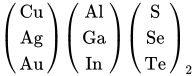


.jpg)


