The
circled dot was used by the Pythagoreans and later Greeks to represent
the first metaphysical being and the metaphysical life, the Monad or the Absolute.
There is something
No experiment could support the hypothesis "There is nothing" because any observation implies the existence of an observer.
Defining the question
The question is usually taken as concerning practical
causality (rather than a moral reason for), and posed totally and
comprehensively, rather than concerning the existence of anything
specific, such as the universe or multiverse, the Big Bang, God, mathematical and physical laws, time or consciousness. It can be seen as an open metaphysical question, rather than a search for an exact answer.
On timescales
The question does not include the timing of when anything came to exist.
Some have suggested the possibility of an infinite regress, where, if an entity cannot come from nothing and this concept is mutually exclusive from something, there must have always been something that caused the previous effect, with this causal chain (either deterministic or probabilistic) extending infinitely back in time.
Arguments against attempting to answer the question
Philosopher Stephen Law has said the question may not need answering, as it is attempting to answer a question that is outside a spacetime setting while being within a spacetime setting. He compares the question to asking "what is north of the North Pole?"
Causation may not apply
The ancient Greek philosopher Aristotle argued that everything in the universe must have a cause, culminating in an ultimate uncaused cause. (See Four causes.)
However, David Hume
argued that a cause may not be necessary in the case of the formation
of the universe. Whilst we expect that everything has a cause because of
our experience for the necessity of causation, the formation of the universe is outside our experience and may be subject to different rules. Kant supported and extended Hume's argument.
We may only say the question because of the nature of our minds
Kant argues that the nature of our mind may lead us to ask
some questions (rather than asking because of the validity of those
questions).
In philosophy, the brute fact approach proposes that some facts cannot be explained in terms of a deeper, more "fundamental" fact. It is in opposition to the principle of sufficient reason approach.
On this question, Bertrand Russell took a brute fact position when he said, "I should say that the universe is just there, and that's all." Sean Carroll
similarly concluded that "any attempt to account for the existence of
something rather than nothing must ultimately bottom out in a set of
brute facts; the universe simply is, without ultimate cause or
explanation."
The question may be impossible to answer
Roy Sorensen has discussed that the question may have an impossible explanatory demand, if there are no existential premises.
Explanations
Something may exist necessarily
Philosopher Brian Leftow has argued that the question cannot have a causal explanation (as any cause must itself have a cause) or a contingent
explanation (as the factors giving the contingency must pre-exist), and
that if there is an answer, it must be something that exists
necessarily (i.e., something that just exists, rather than is caused).
Natural laws may necessarily exist, and may enable the emergence of matter
"Why
is there something rather than nothing? The sufficient reason... is
found in a substance which... is a necessary being bearing the reason
for its existence within itself."
A state of nothing may be impossible
Parmenides questioned whether it was possible for there to be nothing
Nobel Laureate Frank Wilczek is credited with the aphorism that "nothing is unstable." Physicist Sean Carroll argues that this accounts merely for the existence of matter, but not the existence of quantum states, space-time, or the universe as a whole.
Some cosmologists believe it to be possible that something (e.g., the universe)
may come to exist spontaneously from nothing. Some mathematical models
support this idea, and it has been a more prevalent explanation among
the scientific community for why the Big Bang occurred.
Self-Subsumption: "a law that applies to itself, and hence explains its own truth."
The Nothingness Force: "the nothingness force acts on itself, it sucks nothingness into nothingness and produces something..."
Mariusz Stanowski explained: "There must be both something and nothing, because separately neither can be distinguished".
Humour
Philosophical wit Sidney Morgenbesser answered the question with an apothegm: "If there were nothing, you'd still be complaining!", or "Even if there was nothing, you still wouldn't be satisfied!"
In 1948, John Bardeen and Walter Brattain,
the original inventors of transistor technology, patented an
insulated-gate transistor (IGFET) with an inversion layer. Bardeen's
concept forms the basis of CMOS technology today. The CMOS process was
presented by Fairchild Semiconductor's Frank Wanlass and Chih-Tang Sah at the International Solid-State Circuits Conference in 1963. Wanlass later filed US patent 3,356,858 for CMOS circuitry and it was granted in 1967. RCA
commercialized the technology with the trademark "COS-MOS" in the late
1960s, forcing other manufacturers to find another name, leading to
"CMOS" becoming the standard name for the technology by the early 1970s.
Two important characteristics of CMOS devices are high noise immunity and low static power consumption. Since one transistor
of the MOSFET pair is always off, the series combination draws
significant power only momentarily during switching between on and off
states. Consequently, CMOS devices do not produce as much waste heat as other forms of logic, like NMOS logic or transistor–transistor logic
(TTL), which normally have some standing current even when not changing
state. These characteristics allow CMOS to integrate a high density of
logic functions on a chip. It was primarily for this reason that CMOS
became the most widely used technology to be implemented in VLSI chips.
The phrase "metal–oxide–semiconductor" is a reference to the physical structure of MOS field-effect transistors, having a metal gate electrode placed on top of an oxide insulator, which in turn is on top of a semiconductor material. Aluminium was once used but now the material is polysilicon. Other metal gates have made a comeback with the advent of high-κ dielectric materials in the CMOS process, as announced by IBM and Intel for the 45 nanometer node and smaller sizes.
1957 diagram of one of the transistor devices made by Frosch and Derick
The principle of complementary symmetry was first introduced by George Sziklai in 1953 who then discussed several complementary bipolar circuits. Paul Weimer, also at RCA, invented in 1962 thin-film transistor (TFT) complementary circuits, a close relative of CMOS. He invented complementary flip-flop
and inverter circuits, but did no work in a more complex complementary
logic. He was the first person able to put p-channel and n-channel TFTs
in a circuit on the same substrate. Three years earlier, John T. Wallmark and Sanford M. Marcus published a variety of complex logic functions implemented as integrated circuits using JFETs, including complementary memory circuits. Frank Wanlass was familiar with work done by Weimer at RCA.
In 1955, Carl Frosch
and Lincoln Derick accidentally grew a layer of silicon dioxide over
the silicon wafer, for which they observed surface passivation effects. By 1957, Frosch and Derick, using masking and predeposition, were able
to manufacture silicon transistors. They showed that silicon dioxide
protected silicon wafers from dopants diffusing into the wafer, and
insulated the wafer from damage due to heat during the process. J.R. Ligenza and W.G. Spitzer studied the mechanism of thermally grown oxides and fabricated a high quality Si/SiO2 stack in 1960.
Simulation of formation of inversion channel (electron density) and attainment of threshold voltage (IV) in a nanowire MOSFET. Threshold voltage for this device lies around 0.45V.
Following this research, Mohamed Atalla and Dawon Kahng proposed a silicon MOS transistor in 1959 and successfully demonstrated a working MOS device with their Bell Labs team in 1960.Their team included E. E. LaBate and E. I. Povilonis who fabricated the
device; M. O. Thurston, L. A. D'Asaro, and J. R. Ligenza who developed
the diffusion processes, and H. K. Gummel and R. Lindner who
characterized the device. There were originally two types of MOSFET logic, PMOS (p-type MOS) and NMOS (n-type MOS).
In 1948, Bardeen and Brattain patented the progenitor of
MOSFET, an insulated-gate FET (IGFET) with an inversion layer. Bardeen's
patent, and the concept of an inversion layer, forms the basis of CMOS
technology today. A new type of MOSFET logic combining both the PMOS and NMOS processes
was developed, called complementary MOS (CMOS), by Chih-Tang Sah and Frank Wanlass at Fairchild. In February 1963, they published the invention in a research paper. In both the research paper and the patent filed by Wanlass, the fabrication of CMOS devices was outlined, on the basis of thermal oxidation of a silicon substrate to yield a layer of silicon dioxide located between the drain contact and the source contact.
CMOS technology was initially overlooked by the American semiconductor industry
in favour of NMOS, which was more powerful at the time. However, CMOS
was quickly adopted and further advanced by Japanese semiconductor
manufacturers due to its low power consumption, leading to the rise of
the Japanese semiconductor industry. Toshiba developed C2MOS (clocked CMOS), a circuit technology with lower power consumption and faster operating speed than ordinary CMOS, in 1969. Toshiba used its C2MOS technology to develop a large-scale integration (LSI) chip for Sharp's Elsi Mini LEDpocket calculator, developed in 1971 and released in 1972. Suwa Seikosha (now Seiko Epson) began developing a CMOS IC chip for a Seikoquartz watch in 1969, and began mass-production with the launch of the Seiko Analog Quartz 38SQW watch in 1971. The first mass-produced CMOS consumer electronic product was the Hamilton Pulsar "Wrist Computer" digital watch, released in 1970. Due to low power consumption, CMOS logic has been widely used for calculators and watches since the 1970s.
The earliest microprocessors in the early 1970s were PMOS processors, which initially dominated the early microprocessor industry. By the late 1970s, NMOS microprocessors had overtaken PMOS processors. CMOS microprocessors were introduced in 1975, with the Intersil 6100, and RCA CDP 1801. However, CMOS processors did not become dominant until the 1980s.
CMOS was initially slower than NMOS logic, thus NMOS was more widely used for computers in the 1970s. The Intel 5101 (1kbSRAM) CMOS memory chip (1974) had an access time of 800ns,whereas the fastest NMOS chip at the time, the Intel 2147 (4kb SRAM) HMOS memory chip (1976), had an access time of 55/70ns. In 1978, a Hitachi research team led by Toshiaki Masuhara introduced the twin-well Hi-CMOS process, with its HM6147 (4kb SRAM) memory chip, manufactured with a 3 μm process. The Hitachi HM6147 chip was able to match the performance (55/70ns access) of the Intel 2147 HMOS chip, while the HM6147 also consumed significantly less power (15mA) than the 2147 (110mA).
With comparable performance and much less power consumption, the
twin-well CMOS process eventually overtook NMOS as the most common semiconductor manufacturing process for computers in the 1980s.
In the 1980s, CMOS microprocessors overtook NMOS microprocessors. NASA's Galileo spacecraft, sent to orbit Jupiter in 1989, used the RCA 1802 CMOS microprocessor due to low power consumption.
Fujitsu commercialized a 700nm CMOS process in 1987, and then Hitachi, Mitsubishi Electric, NEC and Toshiba commercialized 500nm CMOS in 1989. In 1993, Sony commercialized a 350nm CMOS process, while Hitachi and NEC commercialized 250nm CMOS. Hitachi introduced a 160nm CMOS process in 1995, then Mitsubishi introduced 150nm CMOS in 1996, and then Samsung Electronics introduced 140nm in 1999.
CMOS is used in most modern LSI and VLSI devices. As of 2010, CPUs with the best performance per watt each year have been CMOS static logic since 1976. As of 2019, planar CMOS technology is still the most common form of
semiconductor device fabrication, but is gradually being replaced by
non-planar FinFET technology, which is capable of manufacturing semiconductor nodes smaller than 20nm.
"CMOS" refers to both a particular style of digital
circuitry design and the family of processes used to implement that
circuitry on integrated circuits (chips). CMOS circuitry dissipates less power than logic families
with resistive loads. Since this advantage has increased and grown more
important, CMOS processes and variants have come to dominate, thus the
vast majority of modern integrated circuit manufacturing is on CMOS
processes. CMOS logic consumes around one seventh the power of NMOS logic, and about 10 million times less power than bipolar transistor–transistor logic (TTL).
CMOS circuits use a combination of p-type and n-type metal–oxide–semiconductor field-effect transistor (MOSFETs) to implement logic gates
and other digital circuits. Although CMOS logic can be implemented with
discrete devices for demonstrations, commercial CMOS products are
integrated circuits composed of up to billions of transistors of both
types, on a rectangular piece of silicon of often between 10 and 400mm2.
CMOS always uses all enhancement-mode MOSFETs (in other words, a zero gate-to-source voltage turns the transistor off).
Inversion
CMOS circuits are constructed in such a way that all p-type metal–oxide–semiconductor (PMOS) transistors must have either an input from the voltage source or from another PMOS transistor. Similarly, all NMOS
transistors must have either an input from ground or from another NMOS
transistor. The composition of a PMOS transistor creates low resistance between its source and drain contacts when a low gate voltage
is applied and high resistance when a high gate voltage is applied. On
the other hand, the composition of an NMOS transistor creates high
resistance between source and drain when a low gate voltage is applied
and low resistance when a high gate voltage is applied. CMOS
accomplishes current reduction by complementing every nMOSFET with a
pMOSFET and connecting both gates and both drains together. A high
voltage on the gates will cause the nMOSFET to conduct and the pMOSFET
not to conduct, while a low voltage on the gates causes the reverse.
This arrangement greatly reduces power consumption and heat generation.
However, during the switching time, both pMOS and nMOS MOSFETs conduct
briefly as the gate voltage transitions from one state to another. This
induces a brief spike in power consumption and becomes a serious issue
at high frequencies.
Static CMOS inverter. Vdd and Vss stand for drain and source, respectively.
The adjacent image shows what happens when an input is
connected to both a PMOS transistor (top of diagram) and an NMOS
transistor (bottom of diagram). Vdd is some positive voltage connected
to a power supply and Vss is ground. A is the input and Q is the output.
When the voltage of A is low (i.e. close to Vss), the NMOS
transistor's channel is in a high resistance state, disconnecting Vss
from Q. The PMOS transistor's channel is in a low resistance state,
connecting Vdd to Q. Q, therefore, registers Vdd.
On the other hand, when the voltage of A is high (i.e.
close to Vdd), the PMOS transistor is in a high resistance state,
disconnecting Vdd from Q. The NMOS transistor is in a low resistance
state, connecting Vss to Q. Now, Q registers Vss.
In short, the outputs of the PMOS and NMOS transistors are
complementary such that when the input is low, the output is high, and
when the input is high, the output is low. No matter what the input is,
the output is never left floating (charge is never stored due to wire
capacitance and lack of electrical drain/ground). Because of this
behavior of input and output, the CMOS circuit's output is the inverse
of the input.
The transistors' resistances are never exactly equal to
zero or infinity, so Q will never exactly equal Vss or Vdd, but Q will
always be closer to Vss than A was to Vdd (or vice versa if A were close
to Vss). Without this amplification, there would be a very low limit to
the number of logic gates that could be chained together in series, and
CMOS logic with billions of transistors would be impossible.
The power supply pins for CMOS are called VDD and VSS, or VCC and ground (GND) depending on the manufacturer. VDD and VSS are carryovers from conventional MOS circuits and stand for the drain and source supplies. These do not apply directly to CMOS, since both supplies are really source supplies. VCC and ground are carryovers from TTL logic and that nomenclature has been retained with the introduction of the 54C/74C line of CMOS.
Duality
An important characteristic of a CMOS circuit is the
duality that exists between its PMOS transistors and NMOS transistors. A
CMOS circuit is created to allow a path always to exist from the output
to either the power source or ground. To accomplish this, the set of
all paths to the voltage source must be the complement
of the set of all paths to ground. This can be easily accomplished by
defining one in terms of the NOT of the other. Due to the logic based on
De Morgan's laws,
the PMOS transistors in parallel have corresponding NMOS transistors in
series while the PMOS transistors in series have corresponding NMOS
transistors in parallel.
More complex logic functions such as those involving AND and OR gates
require manipulating the paths between gates to represent the logic.
When a path consists of two transistors in series, both transistors must
have low resistance to the corresponding supply voltage, modelling an
AND. When a path consists of two transistors in parallel, either one or
both of the transistors must have low resistance to connect the supply
voltage to the output, modelling an OR.
Shown on the right is a circuit diagram of a NAND gate
in CMOS logic. If both of the A and B inputs are high, then both the
NMOS transistors (bottom half of the diagram) will conduct, neither of
the PMOS transistors (top half) will conduct, and a conductive path will
be established between the output and Vss
(ground), bringing the output low. If both of the A and B inputs are
low, then neither of the NMOS transistors will conduct, while both of
the PMOS transistors will conduct, establishing a conductive path
between the output and Vdd
(voltage source), bringing the output high. If either of the A or B
inputs is low, one of the NMOS transistors will not conduct, one of the
PMOS transistors will, and a conductive path will be established between
the output and Vdd (voltage
source), bringing the output high. As the only configuration of the two
inputs that results in a low output is when both are high, this circuit
implements a NAND (NOT AND) logic gate.
An advantage of CMOS over NMOS logic is that both
low-to-high and high-to-low output transitions are fast since the (PMOS)
pull-up transistors have low resistance when switched on, unlike the
load resistors in NMOS logic. In addition, the output signal swings the
full voltage between the low and high rails. This strong, more nearly symmetric response also makes CMOS more resistant to noise.
See Logical effort for a method of calculating delay in a CMOS circuit.
Example: NAND gate in physical layout
The physical layout
of a NAND circuit. The larger regions of n-type diffusion and p-type
diffusion are part of the transistors. The two smaller regions on the
left are taps to prevent latchup. Simplified process of fabrication of a CMOS inverter on p-type substrate in semiconductor microfabrication. In step 1, silicon dioxide layers are formed initially through thermal oxidation Note: gate, source and drain contacts are not normally in the same plane in real devices, and the diagram is not to scale.
This example shows a NAND
logic device drawn as a physical representation as it would be
manufactured. The physical layout perspective is a "bird's eye view" of a
stack of layers. The circuit is constructed on a p-type substrate. The polysilicon,
diffusion, and n-well are referred to as "base layers" and are actually
inserted into trenches of the p-type substrate. (See steps 1 to 6 in
the process diagram below right) The contacts penetrate an insulating
layer between the base layers and the first layer of metal (metal1)
making a connection.
The inputs to the NAND
(illustrated in green color) are in polysilicon. The transistors
(devices) are formed by the intersection of the polysilicon and
diffusion; N diffusion for the N device & P diffusion for the P
device (illustrated in salmon and yellow coloring respectively). The
output ("out") is connected together in metal (illustrated in cyan
coloring). Connections between metal and polysilicon or diffusion are
made through contacts (illustrated as black squares). The physical layout example matches the NAND logic circuit given in the previous example.
The N device is manufactured on a p-type substrate while the P device is manufactured in an n-type well (n-well). A p-type substrate "tap" is connected to VSS and an n-type n-well tap is connected to VDD to prevent latchup.
Cross section of two transistors in a CMOS gate, in an n-well CMOS process
Power: switching and leakage
CMOS logic dissipates less power than NMOS logic circuits
because CMOS dissipates power only when switching ("dynamic power"). On a
typical ASIC in a modern 90 nanometer
process, switching the output might take 120 picoseconds, and happens
once every ten nanoseconds. NMOS logic dissipates power whenever the
transistor is on, because there is a current path from Vdd to Vss through the load resistor and the n-type network.
Static CMOS gates are very power efficient because they
dissipate nearly zero power when idle. Earlier, the power consumption of
CMOS devices was not the major concern while designing chips. Factors
like speed and area dominated the design parameters. As the CMOS
technology moved below sub-micron levels the power consumption per unit
area of the chip has risen tremendously.
Broadly classifying, power dissipation in CMOS circuits occurs because of two components, static and dynamic:
Static dissipation
Both NMOS and PMOS transistors have a gate–source threshold voltage (Vth), below which the current (called sub threshold
current) through the device will drop exponentially. Historically, CMOS
circuits operated at supply voltages much larger than their threshold
voltages (Vdd might have been 5V, and Vth for both NMOS and PMOS might have been 700mV). A special type of the transistor used in some CMOS circuits is the native transistor, with near zero threshold voltage.
SiO2 is a good insulator, but at
very small thickness levels electrons can tunnel across the very thin
insulation; the probability drops off exponentially with oxide
thickness. Tunnelling current becomes very important for transistors
below 130nm technology with gate oxides of 20Å or thinner.
Small reverse leakage currents are formed due to formation
of reverse bias between diffusion regions and wells (for e.g., p-type
diffusion vs. n-well), wells and substrate (for e.g., n-well vs.
p-substrate). In modern process diode leakage is very small compared to
sub threshold and tunnelling currents, so these may be neglected during
power calculations.
If the ratios do not match, then there might be different
currents of PMOS and NMOS; this may lead to imbalance and thus improper
current causes the CMOS to heat up and dissipate power unnecessarily.
Furthermore, recent studies have shown that leakage power reduces due to
aging effects as a trade-off for devices to become slower.
To speed up designs, manufacturers have switched to
constructions that have lower voltage thresholds but because of this a
modern NMOS transistor with a Vth of 200mV has a significant subthreshold leakage
current. Designs (e.g. desktop processors) which include vast numbers
of circuits which are not actively switching still consume power because
of this leakage current. Leakage power is a significant portion of the
total power consumed by such designs. Multi-threshold CMOS (MTCMOS), now available from foundries, is one approach to managing leakage power. With MTCMOS, high Vth transistors are used when switching speed is not critical, while low Vth
transistors are used in speed sensitive paths. Further technology
advances that use even thinner gate dielectrics have an additional leakage component because of current tunnelling through the extremely thin gate dielectric. Using high-κ dielectrics instead of silicon dioxide
that is the conventional gate dielectric allows similar device
performance, but with a thicker gate insulator, thus avoiding this
current. Leakage power reduction using new material and system designs
is critical to sustaining scaling of CMOS.
Dynamic dissipation
Charging and discharging of load capacitances
CMOS circuits dissipate power by charging the various load
capacitances (mostly gate and wire capacitance, but also drain and some
source capacitances) whenever they are switched. In one complete cycle
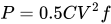
of CMOS logic, current flows from VDD to the load capacitance to charge it and then flows from the charged load capacitance (CL) to ground during discharge. Therefore, in one complete charge/discharge cycle, a total of Q=CLVDD is thus transferred from VDD
to ground. Multiply by the switching frequency on the load capacitances
to get the current used, and multiply by the average voltage again to
get the characteristic switching power dissipated by a CMOS device: .
Since most gates do not operate/switch at every clock cycle, they are often accompanied by a factor , called the activity factor. Now, the dynamic power dissipation may be re-written as .
A clock in a system has an activity factor α=1, since it rises and falls every cycle. Most data has an activity factor of 0.1. If correct load capacitance is estimated on a node together with its
activity factor, the dynamic power dissipation at that node can be
calculated effectively.
Short-circuit power
Since there is a finite rise/fall time for both pMOS and
nMOS, during transition, for example, from off to on, both the
transistors will be on for a small period of time in which current will
find a path directly from VDD to ground, hence creating a short-circuit current, sometimes called a crowbar current. Short-circuit power dissipation increases with the rise and fall time of the transistors.
This form of power consumption became significant in the
1990s as wires on chip became narrower and the long wires became more
resistive. CMOS gates at the end of those resistive wires see slow input
transitions. Careful design which avoids weakly driven long skinny
wires reduces this effect, but crowbar power can be a substantial part
of dynamic CMOS power.
Input protection
Parasitic transistors that are inherent in the CMOS
structure may be turned on by input signals outside the normal operating
range, e.g. electrostatic discharges or line reflections. The resulting latch-up
may damage or destroy the CMOS device. Clamp diodes are included in
CMOS circuits to deal with these signals. Manufacturers' data sheets
specify the maximum permitted current that may flow through the diodes.
Besides digital applications, CMOS technology is also used in analog applications. For example, there are CMOS operational amplifier ICs available in the market. Transmission gates may be used as analog multiplexers instead of signal relays. CMOS technology is also widely used for RF circuits all the way to microwave frequencies, in mixed-signal (analog+digital) applications.
RF CMOS refers to RF circuits (radio frequency circuits) which are based on mixed-signalCMOS integrated circuit technology. They are widely used in wireless telecommunication technology. RF CMOS was developed by Asad Abidi while working at UCLA in the late 1980s. This changed the way in which RF circuits were designed, leading to the replacement of discrete bipolar transistors with CMOS integrated circuits in radiotransceivers. It enabled sophisticated, low-cost and portable end-user
terminals, and gave rise to small, low-cost, low-power and portable
units for a wide range of wireless communication systems. This enabled
"anytime, anywhere" communication and helped bring about the wireless revolution, leading to the rapid growth of the wireless industry.
Examples of commercial RF CMOS chips include Intel's DECT cordless phone, and 802.11 (Wi-Fi) chips created by Atheros and other companies. Commercial RF CMOS products are also used for Bluetooth and wireless LAN (WLAN) networks. RF CMOS is also used in the radio transceivers for wireless standards such as GSM, Wi-Fi, and Bluetooth, transceivers for mobile networks such as 3G, and remote units in wireless sensor networks (WSN).
RF CMOS technology is crucial to modern wireless communications, including wireless networks and mobile communication devices. One of the companies that commercialized RF CMOS technology was Infineon. Its bulk CMOS RF switches sell over 1billion units annually, reaching a cumulative 5billion units, as of 2018.
Temperature range
Conventional CMOS devices work over a range of −55°C to +125°C.
There were theoretical indications as early as August 2008 that silicon CMOS will work down to −233°C (40K). Functioning temperatures near 40K have since been achieved using overclocked AMD Phenom II processors with a combination of liquid nitrogen and liquid helium cooling.
Silicon carbide CMOS devices have been tested for a year at 500°C.
Single-electron MOS transistors
Ultra small (L = 20nm, W = 20nm) MOSFETs achieve the single-electron limit when operated at cryogenic temperature over a range of −269°C (4K) to about −258°C (15K). The transistor displays Coulomb blockade
due to progressive charging of electrons one by one. The number of
electrons confined in the channel is driven by the gate voltage,
starting from an occupation of zero electrons, and it can be set to one
or many.


.jpg)

.jpg)


-Gate_oxide_transistor_by_Frosch_and_Derrick.png)